Äîêóìåíòàöèÿ è îïèñàíèÿ www.docs.chipfind.ru
MM908E622
Rev 1.0, 09/2005
Freescale Semiconductor
Technical Data
This document contains certain information on a new product.
Specifications and information herein are subject to change without notice.
© Freescale Semiconductor, Inc., 2005. All rights reserved.
Integrated Quad Half-Bridge,
Triple High-Side and EC Glass
Driver with Embedded MCU and
LIN for High End Mirror
The 908E622 is an integrated single-package solution that
includes a high-performance HC08 microcontroller with a
SMARTMOS
TM
analog control IC. The HC08 includes flash memory,
a timer, enhanced serial communications interface (ESCI), an
analog-to-digital converter (ADC), serial peripheral interface (SPI)
(only internal), and an internal clock generator module. The analog
control die provides four half-bridge and three high-side outputs with
diagnostic functions, an EC glass driver circuit, a Hall-Effect sensor
input, analog inputs, voltage regulator, window watchdog, and local
interconnect network (LIN) physical layer.
The single-package solution, together with LIN, provides optimal
application performance adjustments and space-saving PCB design.
It is well suited for the control of automotive high-end mirrors.
Features
· High-Performance M68HC908EY16 Core
· 16 K Bytes of On-Chip Flash Memory, 512 Bytes of RAM
· Internal Clock Generator Module (ICG)
· Two 16-Bit, 2-Channel Timers
· 10-Bit Analog-to-Digital Converter (ADC)
· LIN Physical Layer Interface
· Autonomous MCU Watchdog / MCU Supervision
· One Analog Input with Switchable Current Source
· Four Low RDS(ON) Half-Bridge Outputs
· Three Low RDS(ON) High-Side Outputs
· EC glass driver circuitry
· Wake-Up Input
· One 2/3-Pin Hall-Effect Sensor Input
·
12 Microcontroller I/Os
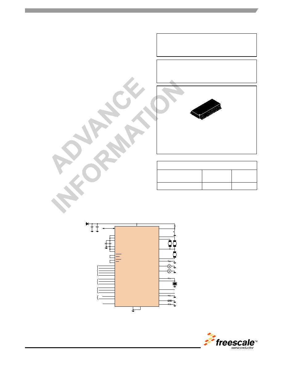
Figure 1. 908E622 Simplified Application Diagram
QUAD HALF-BRIDGE, TRIPLE HIGH-SIDE
SWITCH AND EC GLASS CIRCUITRY WITH
EMBEDDED MCU AND LIN
908E622
ORDERING INFORMATION
Device
Temperature
Range (T
A
)
Package
MM908E622ACDWB/R2
-40°C to 85°C 54 SOICW-EP
DWB SUFFIX
98ARL10519D
54-TERMINAL SOICW-EP
RST_A
RST
IRQ_A
IRQ
VSSA/VREFL
LIN
VDDA/VREFH
EVDD
VDD
EVSS
VSS
L0
HS1
ECR
VSUP[1:8]
A0
A0CST
High Side Output 3
High Side Output 2
High Side Output 1
HS2
HS3
EC
H0
HVDD
GND[1:4]
EC - Glas Control
Switched 5V output
Analog Input with current source
Analog Input current source trim
2-/3-pin hall sensor input
Wake Up Input
4.
7
µF
>2
2µF
HB1
HB2
M
M
4 x Half Bridge Outputs
HB3
M
HB4
PTC2/MCLK
PTC3/OSC2
PTC4/OSC1
µC PortC
PTB3/AD3
PTB4/AD4
PTB5/AD5
µC PortB
PTA0/KBD0
PTA1/KBD1
PTA2/KBD2
PTA3/KBD3
PTA4/KBD4
µC PortA
PTE1/RxD
Internally connected
µC PortE
PTD0/TACH0
µC PortD
PTD1/TACH1
TESTMODE
Pull to ground for user mode
EP
1
00n
F
1
00n
F
Internally connected
908E622
Analog Integrated Circuit Device Data
2
Freescale Semiconductor
908E622
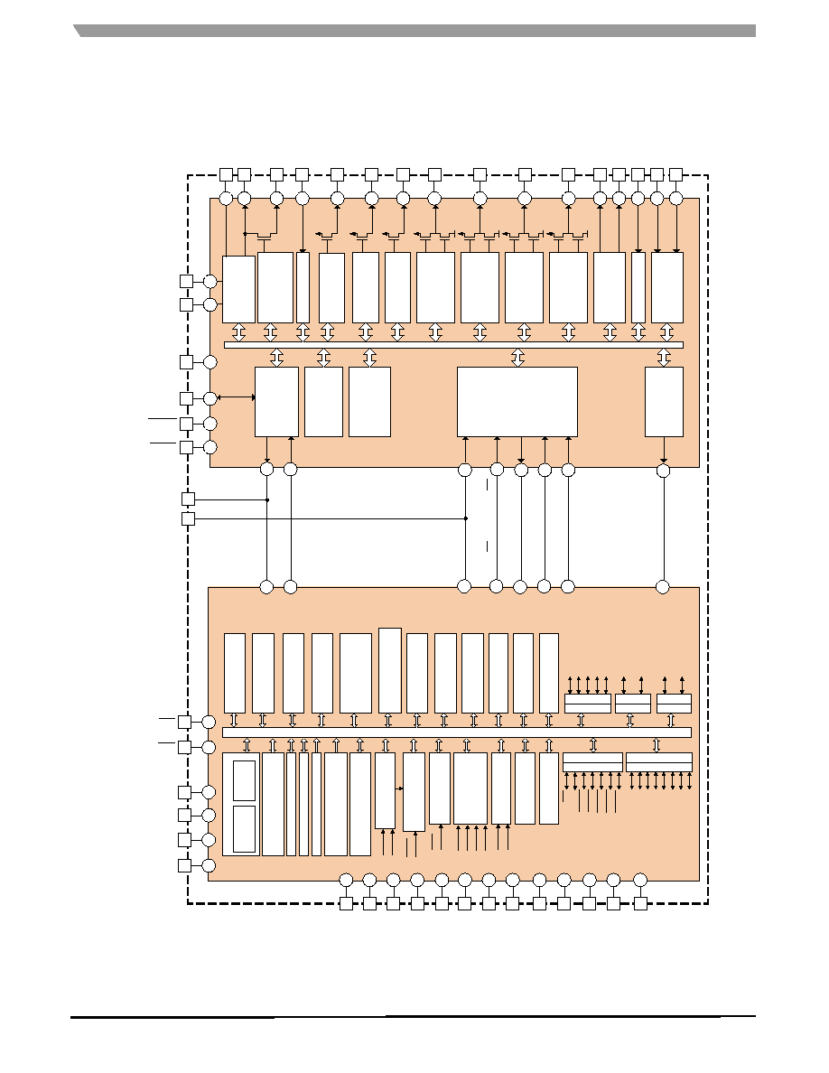
Internal Block Diagram
INTERNAL BLOCK DIAGRAM
M68H
C08 C
P
U
ALU
PORT B
DDRB
PTB0/AD0
ADOUT
Analog
Multiplexer
Analog Port
with Current
Source
CPU
Registers
DDRE
PORT E
PTE1/RXD
PTE0/TXD
PTB1/AD1
PTB2/AD2
PTB3/AD3
PTB4/AD4
PTB5/AD5
PTB6/AD6/TBCH0
PTB7/AD7/TBCH1
DDRD
PORT D
PTD1/TACH1
PTD0/TACH0
PORT C
DDRC
PTC4/OSC1 PTC3/OSC2 PTC2/MCLK PTC1/MOSI PTC0/MISO
BEMF Module
Prescaler Module
Arbiter Module
Periodic Wake-up
Timebase Module
Configuration
Register Module
Serial Peripheral
Interface Module
Computer Operating
Properly Module
Enhanced Serial
Communication
Interface Module
2-channel Timer
Interface Module B
2-channel Timer
Interface Module A
5-Bit Keyboard
Interrupt Module
Single Breakpoint
Break Module
DDRA
PORT A
PTA0/KBD0
PTA1/KBD1
PTA2/KBD2
PTA3/KBD3
PTA4/KBD4
PTA5/SPSCK
PTA6/SS
Security Module
Power-ON
Reset Module
POWER
VSS
VDD
10 Bit Analog-to-
Digital Converter
Module
VSSA
VREFL
VDDA
VREFH
Single External
IRQ Module
IRQ
24 Internal System
Integration Module
RST
Internal Clock
Generator Module
OSC1
OSC2
User Flash Vector
Space, 36 Bytes
Flash programming
(Burn-in), 1024 Bytes
Monitor ROM, 310 Bytes
User RAM, 512 Bytes
User Flash, 15,872 Bytes
Control and Status
Register, 64 Bytes
Internal Bus
FLSVPP
PTD1/TACH1
PTC4/OSC1
PTC3/OSC2
PTC2/MCLK
PTB5/AD5
PTB4/AD4
PTB3/AD3
PTA4/KBD4
PTA3/KBD3
PTA2/KBD2
PTA1/KBD1
PTA0/KBD0
VDDA/VREFH
EVDD
EVSS
VSSA/VREFL
RST
IRQ
RST_A
IRQ_A
PTE1/RXD
PTD0/TACH0
LIN
TESTMODE
VSUP[1:8]
GND[1:4]
PTB0/AD0
PTA5/SPSCK
SPSCK
MOSI
PTC1/MOSI
MISO
PTC0/MISO
SS
PWM
PTA6/SS
PTD0/TACH0
PTE0/TXD
PTE1/RXD
RXD
TXD
SPI
&
CONTROL
Hallport
EC glass Driver
& Diagnostic
Half Bridge
Driver &
Diagnostic
Half Bridge
Driver &
Diagnostic
Half Bridge
Driver &
Diagnostic
Half Bridge
Driver &
Diagnostic
High Side Driver
& Diagnostic
High Side Driver
& Diagnostic
High Side Driver
& Diagnostic
Autonomous
Watchdog
Reset
Control
LIN
Physical Layer
Wakeup Port
Voltage
Regulator
Switched VDD
Driver &
Diagnostic
A0CST
A0
H0
EC
ECR
HB4
HB3
HB2
HB1
HS3
HS2
HS1[a:b]
L0
HVDD
VDD
VSS
Fig
u
re
2
.
90
8E622
Simplifie
d In
tern
al
B
l
o
ck Diag
ram
Analog Integrated Circuit Device Data
Freescale Semiconductor
3
908E622
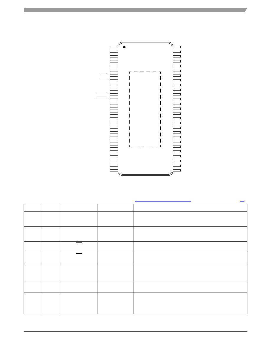
Terminal Connections
TERMINAL CONNECTIONS
Figure 3. Terminal Connections
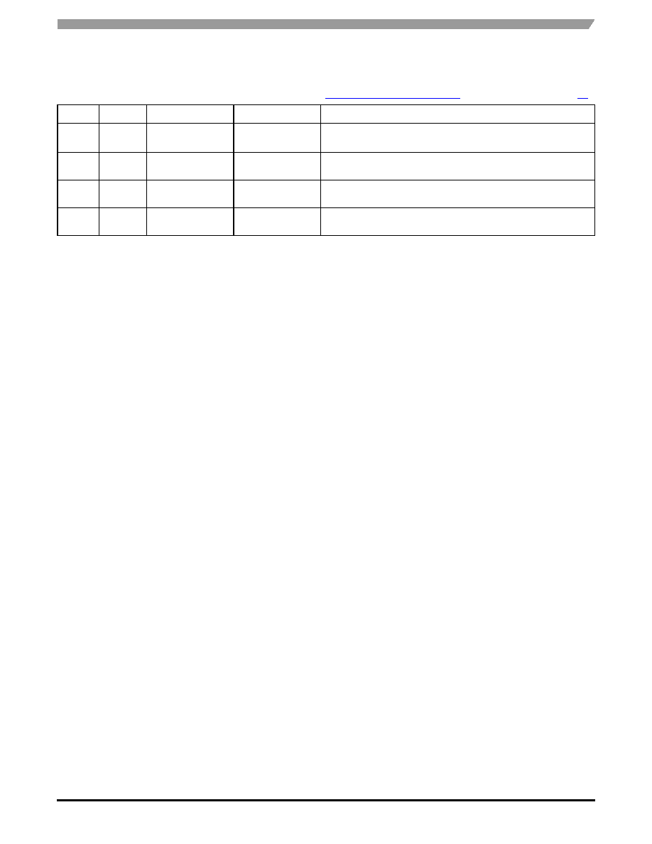
Table 1. Terminal Definitions
A functional description of each terminal can be found in the
Functional Terminal Description
section beginning on page
21
.
Die
Terminal
Terminal Name
Formal Name
Definition
MCU
1
2
3
PTC4/OSC1
PTC3/OSC2
PTC2/MCLK
Port C I/Os
These terminals are special-function, bidirectional I/O port terminals
that are shared with other functional modules in the MCU.
MCU
4
5
6
PTB5/AD5
PTB4/AD4
PTB3/AD3
Port B I/Os
These terminals are special-function, bidirectional I/O port terminals
that are shared with other functional modules in the MCU.
MCU
7
IRQ
External Interrupt
Input
This terminal is an asynchronous external interrupt input terminal.
MCU
8
RST
External Reset
This terminal is bidirectional, allowing a reset of the entire system. It is
driven low when any internal reset source is asserted.
MCU /
Analog
9
(PTD0/TACH0/BEMF
-> PWM)
PWM signal
This terminal is the PWM signal test terminal. It internally connects the
MCU PTD0/TACH0 terminal with the Analog die PWM input.
Note: Do not connect in the application.
MCU
10
PTD1/TACH1
Port D I/Os
This terminal is a special-function, bidirectional I/O port terminal that is
shared with other functional modules in the MCU.
MCU /
Analog
44
(PTE1/RXD <- RXD)
LIN Transceiver
Output
This terminal is the LIN Transceiver output test terminal. It internally
connects the MCU PTE1/RXD terminal with the Analog die LIN
transceiver output terminal RXD.
Note: Do not connect in the application.
PTA0/KBD0
PTA1/KBD1
PTA2/KBD2
PTA3/KBD3
PTA4/KBD4
VDDA/VREFH
EVDD
EVSS
VSSA/VREFL
(PTE1/RXD <- RXD)
VSS
VDD
HVDD
L0
H0
HS3
VSUP8
HS2
VSUP7
HS1b
HS1a
VSUP6
VSUP5
GND4
HB1
VSUP4
FLSVPP
PTC4/OSC1
PTC3/OSC2
PTC2/MCLK
PTB5/AD5
PTB4/AD4
PTB3/AD3
IRQ
RST
(PTD0/TACH0/BEMF -> PWM)
PTD1/TACH1
RST_A
IRQ_A
LIN
A0CST
A0
GND1
HB4
VSUP1
GND2
HB3
VSUP2
EC
ECR
TESTMODE
GND3
HB2
VSUP3
1
11
12
13
14
15
16
17
18
19
20
9
10
21
22
23
24
25
26
27
6
7
8
4
5
2
3
54
44
43
42
41
40
39
38
37
36
35
46
45
34
33
32
31
30
29
28
49
48
47
51
50
53
52
Exposed
Pad
Transparent Top
View of Package
Analog Integrated Circuit Device Data
4
Freescale Semiconductor
908E622
Terminal Connections
MCU
45
48
VSSA/VREFL
VDDA/VREFH
ADC Supply and
Reference Terminals
These terminals
are the power supply and voltage reference terminals
for the analog-to-digital converter (ADC).
MCU
46
47
EVSS
EVDD
MCU Power Supply
Terminals
These terminals are the ground and power supply terminals,
respectively. The MCU operates from a single power supply.
MCU
49
50
52
53
54
PTA4/KBD4
PTA3/KBD3
PTA2/KBD2
PTA1/KBD1
PTA0/KBD0
Port A I/Os
These terminals are special-function, bidirectional I/O port terminals
that are shared with other functional modules in the MCU.
MCU
51
FLSVPP
Test Terminal
For test purposes only. Do not connect in the application.
Analog
11
RST_A
Internal Reset
This terminal is the bidirectional reset terminal of the analog die.
Analog
12
IRQ_A
Internal Interrupt
Output
This terminal is the interrupt output terminal of the analog die indicating
errors or wake-up events.
Analog
13
LIN
LIN Bus
This terminal represents the single-wire bus transmitter and receiver.
Analog
14
A0CST
Analog Input Trim
Terminal
This is the Analog Input Trim Terminal for the A0 input. This is to
connect a known fixed resistor value to trim the current source
measurement.
Analog
15
A0
Analog Input Terminal This terminal is an analog input port with selectable source values.
Analog
16
19
25
30
GND1
GND2
GND3
GND4
Power Ground
Terminals
These terminals are device power ground connections.
Analog
29
26
20
17
HB1
HB2
HB3
HB4
Half-Bridge Outputs
This device includes power MOSFETs configured as four half-bridge
driver outputs. These outputs may be configured for DC motor drivers,
or as high-side and low-side switches.
Note: The HB3 and HB4 have a lower R
DS(ON)
then HB1 and HB2.
Analog
18
21
27
28
31
32
35
VSUP1
VSUP2
VSUP3
VSUP4
VSUP5
VSUP6
VSUP7
Power Supply
Terminals
These terminals are device power supply terminals.
Analog
22
23
EC
ECR
EC Glass Terminal
EC Ballast Resistor
Terminal
These are the Electrochrome Circuitry Terminals. The EC Terminal has
to be connected to the EC Glass and the ECR Terminal has to be
connected to the external ballast resistor.
Analog
24
TESTMODE
TESTMODE Input
Terminal for test purpose only. In application this terminal needs to be
tied GND.
Analog
34
35
HS1a
HS1b
High-Side HS1
Output
This output terminal is a low R
DS(ON)
high-side switch.
Analog
36
38
HS2
HS3
High-Side HS2
Output
High-Side HS3
Output
These output terminals are low R
DS(ON)
high-side switches.
Analog
39
H0
Hall-Effect Sensor /
General Purpose
Input
This terminal provides an input for a Hall-effect sensor or general
purpose input.
Analog
40
L0
Wake-up Input
This terminal provides an high voltage input, which is wake-up capable.
Table 1. Terminal Definitions (continued)
A functional description of each terminal can be found in the
Functional Terminal Description
section beginning on page
21
.
Die
Terminal
Terminal Name
Formal Name
Definition
Analog Integrated Circuit Device Data
Freescale Semiconductor
5
908E622
Terminal Connections
Analog
41
HVDD
Switchable V
DD
Output
This terminal is a switchable V
DD
output for driving resistive loads
requiring a regulated 5.0 V supply; e.g. potentiometers.
Analog
42
VDD
Voltage Regulator
Output
The +5.0 V voltage regulator output terminal is intended to supply the
embedded microcontroller.
Analog
43
VSS
Voltage Regulator
Ground
Ground terminal for the connection of all non-power ground connections
(microcontroller and sensors).
EP
Exposed Pad
Exposed Pad
The exposed pad terminal on the bottom side of the package conducts
heat from the chip to the PCB board.
Table 1. Terminal Definitions (continued)
A functional description of each terminal can be found in the
Functional Terminal Description
section beginning on page
21
.
Die
Terminal
Terminal Name
Formal Name
Definition
Document Outline