Äîêóìåíòàöèÿ è îïèñàíèÿ www.docs.chipfind.ru
MOTOROLA
SEMICONDUCTOR TECHNICAL DATA
Order Number: MMA2204D
Rev. 1, 06/2004
© Motorola, Inc. 2004
REV 1
Surface Mount
Micromachined Accelerometer
The MMA series of silicon capacitive, micromachined accelerometers features
signal conditioning, a 4-pole low pass filter and temperature compensation. Zero-g
offset full scale span and filter cut-off are factory set and require no external devices.
A full system self-test capability verifies system functionality.
Features
·
Integral Signal Conditioning
·
Linear Output
·
Ratiometric Performance
·
4th Order Bessel Filter Preserves Pulse Shape Integrity
·
Calibrated Self-test
·
Low Voltage Detect, Clock Monitor, and EPROM Parity Check Status
·
Transducer Hermetically Sealed at Wafer Level for Superior Reliability
·
Robust Design, High Shocks Survivability
Typical Applications
·
Vibration Monitoring and Recording
·
Appliance Control
·
Mechanical Bearing Monitoring
·
Computer Hard Drive Protection
·
Computer Mouse and Joysticks
·
Virtual Reality Input Devices
·
Sport Diagnostic Devices and Systems
ORDERING INFORMATION
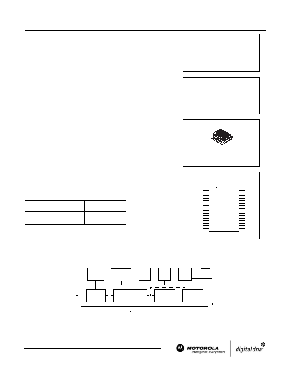
Figure 1. Simplified Accelerometer Functional Block Diagram
Device
Temperature
Range
Package
MMA2204D
40 to +125°C SOIC-16
MMA2204DR2
40 to +125°C SOIC-16, Tape & Reel
MMA2204D
16 LEAD SOIC
CASE 475-01
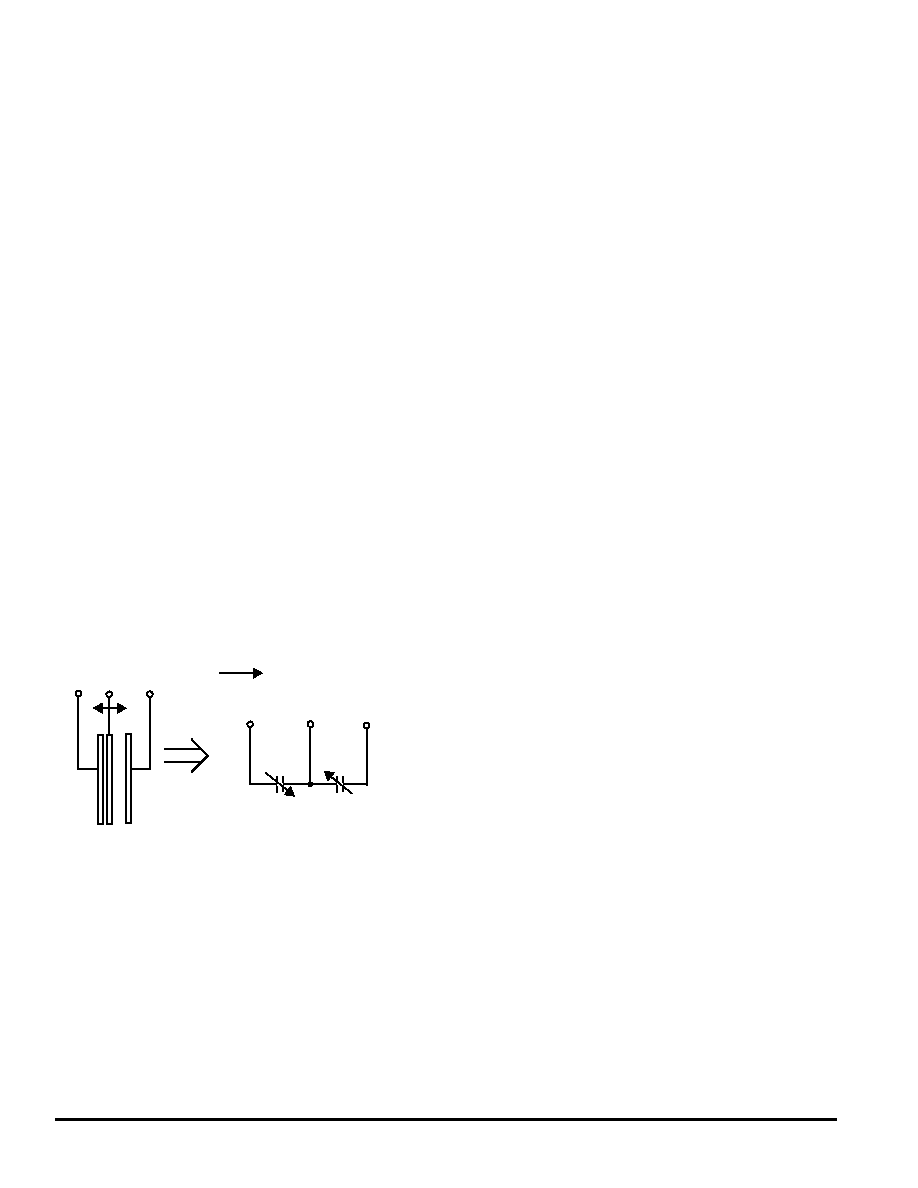
PIN ASSIGNMENT
N/C
N/C
N/C
ST
V
OUT
STATUS
V
SS
V
DD
N/C
N/C
N/C
N/C
N/C
N/C
N/C
N/C
1
2
3
4
5
6
7
8
16
15
14
13
12
11
10
9
MMA2204D: X AXIS SENSITIVITY
MICROMACHINED
ACCELEROMETER
±100g
G-Cell
Sensor
In
tegrator
Gain
Filter
Temp
Comp
S
elf-test
Control Logic &
EPROM
Trim Circuits
Clock
Gen.
Oscillator
V
DD
V
OUT
V
SS
V
ST
Status
F
r
e
e
s
c
a
l
e
S
e
m
i
c
o
n
d
u
c
t
o
r
,
I
Freescale Semiconductor, Inc.
For More Information On This Product,
Go to: www.freescale.com
n
c
.
.
.
MMA2204D
Motorola Sensor Device Data
2
Maximum Ratings
(Maximum ratings are the limits to which the device can be exposed without causing permanent damage.)
NOTES:
1. Dropped onto concrete surface from any axis.
ELECTRO STATIC DISCHARGE (ESD)
WARNING: This device is sensitive to electrostatic
discharge.
Although the Motorola accelerometers contain internal 2kV
ESD protection circuitry, extra precaution must be taken by the
user to protect the chip from ESD. A charge of over 2000 volts
can accumulate on the human body or associated test
equipment. A charge of this magnitude can alter the
performance or cause failure of the chip. When handling the
accelerometer, proper ESD precautions should be followed to
avoid exposing the device to discharges which may be
detrimental to its performance.
Rating
Symbol
Value
Unit
Powered Acceleration (all axes)
G
pd
1500
g
Unpowered Acceleration (all axes)
G
upd
2000
g
Supply Voltage
V
DD
0.3 to +7.0
V
Drop Test
(1)
D
drop
1.2
m
Storage Temperature Range
T
stg
40 to +125
°C
F
r
e
e
s
c
a
l
e
S
e
m
i
c
o
n
d
u
c
t
o
r
,
I
Freescale Semiconductor, Inc.
For More Information On This Product,
Go to: www.freescale.com
n
c
.
.
.
Motorola Sensor Device Data
MMA2204D
3
Operating Characteristics
(Unless otherwise noted: 40°C
T
A
+105°C, 4.75
V
DD
5.25, Acceleration = 0g, Loaded output.
(1)
)
NOTES:
1. For a loaded output the measurements are observed after an RC filter consisting of a 1 k
resistor and a 0.01
µ
F capacitor to ground.
2. These limits define the range of operation for which the part will meet specification.
3. Within the supply range of 4.75 and 5.25 volts, the device operates as a fully calibrated linear accelerometer. Beyond these supply limits the device may
operate as a linear device but is not guaranteed to be in calibration.
4. The device can measure both + and acceleration. With no input acceleration the output is at midsupply. For positive acceleration the output will increase
above V
DD
/2 and for negative acceleration the output will decrease below V
DD
/2.
5. The device is calibrated at 20g.
6. At clock frequency
70 kHz.
7. The digital input pin has an internal pull-down current source to prevent inadvertent self test initiation due to external board level leakages.
8. Time for the output to reach 90% of its final value after a self-test is initiated.
9. Time for amplifiers to recover after an acceleration signal causing them to saturate.
10. Preserves phase margin (60°) to guarantee output amplifier stability.
11. A measure of the device's ability to reject an acceleration applied 90° from the true axis of sensitivity.
12. The Status pin output is not valid following power-up until at least one rising edge has been applied to the self-test pin. The Status pin is high whenever
the self-test input is high, as a means to check the connectivity of the self-test and Status pins in the application.
13. The Status pin output latches high if a Low Voltage Detection or Clock Frequency failure occurs, or the EPROM parity changes to odd. The Status pin can
be reset low if the self-test pin is pulsed with a high input for at least 100
µ
s, unless a fault condition continues to exist.
Characteristic
Symbol
Min
Typ
Max
Unit
Operating Range
(2)
Supply Voltage
(3)
Supply Current
Operating Temperature Range
Acceleration Range
V
DD
I
DD
T
A
g
FS
4.75
4.0
-
40
--
5.00
5.0
--
112.5
5.25
6.0
+125
--
V
mA
°
C
g
Output Signal
Zero g (T
A
= 25°C, V
DD
= 5.0 V)
(4)
Zero g
Sensitivity (T
A
= 25°C, V
DD
= 5.0 V)
(5)
Sensitivity
Bandwidth Response
Nonlinearity
V
OFF
V
OFF,V
S
S
V
f
3dB
NL
OUT
2.35
0.46 V
DD
19
3.72
360
1.0
2.5
0.50
V
DD
20
4
400
--
2.65
0.54
V
DD
21
4.28
440
+1.0
V
V
mV/g
mV/g/V
Hz
% FSO
Noise
RMS (.01 Hz 1 kHz)
Power Spectral Density
Clock Noise (without RC load on output)
(6)
n
RMS
n
PSD
n
CLK
--
--
--
--
110
2.0
2.8
--
--
mVrms
µ
V/(Hz
1/2
)
mVpk
Self-Test
Output Response
Input Low
Input High
Input Loading
(7)
Response Time
(8)
g
ST
V
IL
V
IH
I
IN
t
ST
10
V
SS
0.7
×
V
DD
30
--
12
--
--
110
2.0
14
0.3
×
V
DD
V
DD
300
10
g
V
V
µ
A
ms
Status
(12)(13)
Output Low (I
load
= 100
µ
A)
Output High (I
load
= 100
µ
A)
V
OL
V
OH
--
V
DD
0.8
--
--
0.4
--
V
V
Minimum Supply Voltage (LVD Trip)
V
LVD
2.7
3.25
4.0
V
Clock Monitor Fail Detection Frequency
f
min
150
--
400
kHz
Output Stage Performance
Electrical Saturation Recovery Time
(9)
Full Scale Output Range (I
OUT
= 200
µ
A)
Capacitive Load Drive
(10)
Output Impedence
t
DELAY
V
FSO
C
L
Z
O
--
0.25
--
--
0.2
--
--
300
--
V
DD
0.25
100
--
ms
V
pF
W
Mechanical Characteristics
Transverse Sensitivity
(11)
Package Resonance
V
XZ,YZ
f
PKG
--
--
--
10
5.0
--
% FSO
kHz
F
r
e
e
s
c
a
l
e
S
e
m
i
c
o
n
d
u
c
t
o
r
,
I
Freescale Semiconductor, Inc.
For More Information On This Product,
Go to: www.freescale.com
n
c
.
.
.
MMA2204D
Motorola Sensor Device Data
4
PRINCIPLE OF OPERATION
The Motorola accelerometer is a surface-micromachined
integrated-circuit accelerometer.
The device consists of a surface micromachined capacitive
sensing cell (g-cell) and a CMOS signal conditioning ASIC
contained in a single integrated circuit package. The sensing
element is sealed hermetically at the wafer level using a bulk
micromachined "cap'' wafer.
The g-cell is a mechanical structure formed from
semiconductor materials (polysilicon) using semiconductor
processes (masking and etching). It can be modeled as a set of
beams attached to a movable central mass that move between
fixed beans. The movable beams can be deflected from their
rest position by subjecting the system to an acceleration
(Figure 2).
When the beams attached to the center mass move, the
distance from them to the fixed beams on one side will increase
by the same amount that the distance to the fixed beams on the
other side decreases. The change in distance is a measure of
acceleration.
The g-cell beams form two back-to-back capacitors
(Figure 2). As the center plate moves with acceleration, the
distance between the beams change and each capacitor's
value will change, (C = NA
/D). Where A is the area of the
facing side of the beam,
is the dielectric constant, and D is the
distance between the beams, and N is the number of beams.
The CMOS ASIC uses switched capacitor techniques to
measure the g-cell capacitors and extract the acceleration data
from the difference between the two capacitors. The ASIC also
signal conditions and filters (switched capacitor) the signal,
providing a high level output voltage that is ratiometric and
proportional to acceleration.
Figure 2. Simplified Transducer Physical Model
SPECIAL FEATURES
Filtering
The Motorola accelerometers contain an onboard 4-pole
switched capacitor filter. A Bessel implementation is used
because it provides a maximally flat delay response (linear
phase) thus preserving pulse shape integrity. Because the filter
is realized using switched capacitor techniques, there is no
requirement for external passive components (resistors and
capacitors) to set the cut-off frequency.
Self-Test
The sensor provides a self-test feature that allows the
verification of the mechanical and electrical integrity of the
accelerometer at any time before or after installation. This
feature is critical in applications such as automotive airbag
systems where system integrity must be ensured over the life of
the vehicle. A fourth "plate'' is used in the g-cell as a self-test
plate. When the user applies a logic high input to the self-test
pin, a calibrated potential is applied across the self-test plate
and the moveable plate. The resulting electrostatic force
(Fe =
1
/
2
AV
2
/d
2
) causes the center plate to deflect. The
resultant deflection is measured by the accelerometer's control
ASIC and a proportional output voltage results. This procedure
assures that both the mechanical (g-cell) and electronic
sections of the accelerometer are functioning.
Ratiometricity
Ratiometricity simply means that the output offset voltage
and sensitivity will scale linearly with applied supply voltage.
That is, as you increase supply voltage the sensitivity and offset
increase linearly; as supply voltage decreases, offset and
sensitivity decrease linearly. This is a key feature when
interfacing to a microcontroller or an A/D converter because it
provides system level cancellation of supply induced errors in
the analog to digital conversion process.
Status
Motorola accelerometers include fault detection circuitry and
a fault latch. The Status pin is an output from the fault latch,
OR'd with self-test, and is set high whenever one (or more) of
the following events occur:
·
Supply voltage falls below the Low Voltage Detect (LVD)
voltage threshold
·
Clock oscillator falls below the clock monitor minimum
frequency
·
Parity of the EPROM bits becomes odd in number.
The fault latch can be reset by a falling edge on the self-test
input pin, unless one (or more) of the fault conditions continues
to exist.
Acceleration
F
r
e
e
s
c
a
l
e
S
e
m
i
c
o
n
d
u
c
t
o
r
,
I
Freescale Semiconductor, Inc.
For More Information On This Product,
Go to: www.freescale.com
n
c
.
.
.
Motorola Sensor Device Data
MMA2204D
5
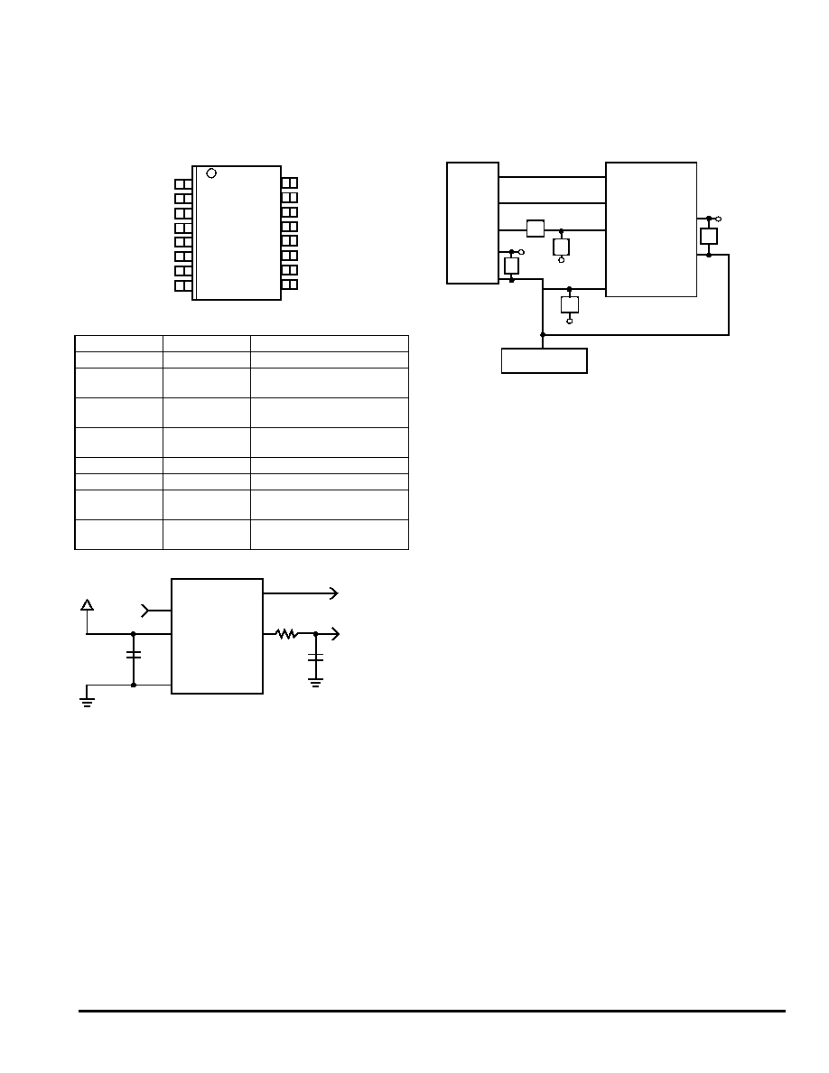
BASIC CONNECTIONS
Pinout Description
Figure 3. SOIC Accelerometer with Recommended
Connection Diagram
Figure 4. Recommended PCB Layout for Interfacing
Accelerometer to Microcontroller
NOTES:
·
Use a 0.1
µ
F capacitor on VDD to decouple the power
source.
·
Physical coupling distance of the accelerometer to the
microcontroller should be minimal.
·
Place a ground plane beneath the accelerometer to reduce
noise, the ground plane should be attached to all of the open
ended terminals shown in Figure 4.
·
Use an RC filter of 1 k
and 0.01
µ
F on the output of the
accelerometer to minimize clock noise (from the switched
capacitor filter circuit).
·
PCB layout of power and ground should not couple power
supply noise.
·
Accelerometer and microcontroller should not be a high
current path.
·
A/D sampling rate and any external power supply switching
frequency should be selected such that they do not interfere
with the internal accelerometer sampling frequency. This
will prevent aliasing errors.
Pin No.
Pin Name
Description
1 thru 3
--
Leave unconnected.
4
ST
Logic input pin used to initiate
self-test.
5
V
OUT
Output voltage of the
accelerometer.
6
STATUS
Logic output pin to indicate
fault.
7
V
SS
The power supply ground.
8
V
DD
The power supply input.
9 thru 13
Trim pins
Used for factory trim. Leave
unconnected.
14 thru 16
--
No internal connection. Leave
unconnected.
N/C
N/C
N/C
ST
V
OUT
STATUS
V
SS
V
DD
N/C
N/C
N/C
N/C
N/C
N/C
N/C
N/C
1
2
3
4
5
6
7
8
16
15
14
13
12
11
10
9
MMA2204D
ST
V
OUT
Output
Signal
R1
1 k
5
C2
0.01
µF
4
7
Logic
Input
V
DD
C1
0.1
µF
6
Status
8 V
DD
V
SS
P0
A/D In
V
RH
V
SS
V
DD
ST
V
OUT
V
SS
V
DD
0.01
µF
1 k
0
.1
µF
0.1
µF
Power Supply
0.1
µF
P1
STATUS
Mic
r
oc
on
trol
ler
Ac
ce
ler
o
m
e
t
e
r
C
R
R
C
C
C
F
r
e
e
s
c
a
l
e
S
e
m
i
c
o
n
d
u
c
t
o
r
,
I
Freescale Semiconductor, Inc.
For More Information On This Product,
Go to: www.freescale.com
n
c
.
.
.
Document Outline