MMA6270Q
Rev 1.0 2/2006
Freescale Semiconductor
Technical Data
© Freescale Semiconductor, Inc., 2006. All rights reserved.
±
1.5 g - 6 g Dual Axis Low-g
Micromachined Accelerometer
The MMA6270Q low cost capacitive micromachined accelerometer features
signal conditioning, a 1-pole low pass filter, temperature compensation and g-
Select which allows for the selection among four sensitivities. Zero-g offset full
scale span and filter cut-off are factory set and require no external devices.
Includes a Sleep Mode that makes it ideal for handheld battery powered
electronics.
Features
∑
Selectable Sensitivity (1.5 g / 2 g / 4 g / 6 g)
∑
Low Current Consumption: 500
µ
A
∑
Sleep Mode: 3
µ
A
∑
Low Voltage Operation: 2.2 V ≠ 3.6 V
∑
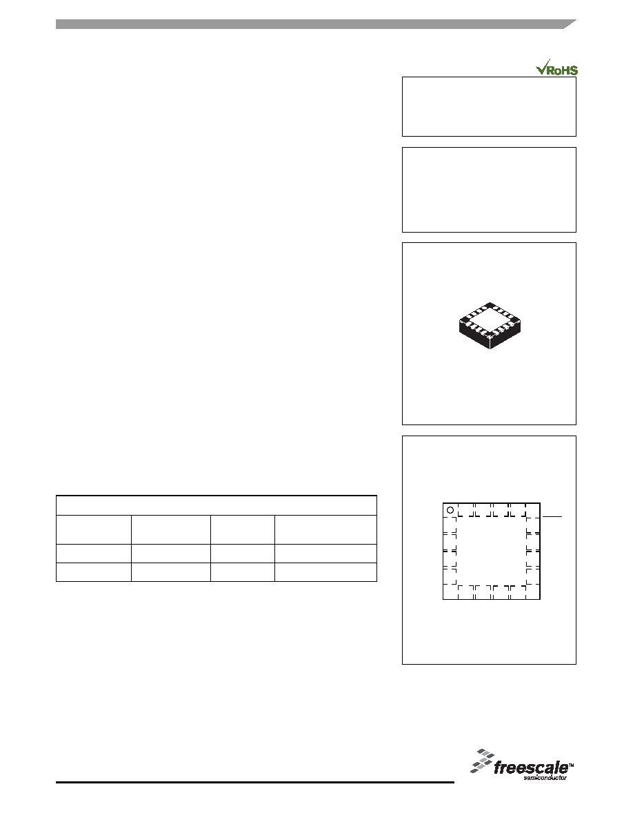
6 mm x 6 mm x 1.45 mm QFN
∑
High Sensitivity (800 mV/g @1.5 g)
∑
Fast Turn On Time
∑
Integral Signal Conditioning with Low Pass Filter
∑
Robust Design, High Shocks Survivability
∑
Pb-Free Terminations
∑
Environmentally Preferred Package
∑
Low Cost
Typical Applications
∑
Laptop PC: Freefall Detection, Anti-Theft
∑
Cell Phone: Image Stability, Text Scroll, Motion Dialing, E-Compass
∑
PDA: Text Scroll
∑
Navigation and Dead Reckoning: E-Compass Tilt Compensation
∑
Gaming: Tilt and Motion Sensing, Event Recorder
∑
Robotics: Motion Sensing
∑
Appliances: Vibration Sensing
ORDERING INFORMATION
Device Name
Temperature
Range
Package
Drawing
Package
MMA6270Q
≠ 20 to +85∞C
98ASA10651D
QFN-16, Tube
MMA6270QR2
≠ 20 to +85∞C
98ASA10651D
QFN-16,Tape & Reel
MMA6270Q
MMA6270Q: XY AXIS
ACCELEROMETER
±
1.5 g / 2 g / 4 g / 6 g
16 LEAD
QFN
98ASA10651D
16
15
14
13
5
6
7
8
1
2
3
4
12
11
10
9
g-Select1
g-Select2
V
DD
V
SS
Sleep
Mode
N/C
N/C
N/C
N/C
N/C
N/C
N/C
N/
C
X
OUT
Y
OUT
N/
C
Bottom View
Figure 1. Pin Connections
Top View
Analog Integrated Circuit Device Data
2
Freescale Semiconductor
MMA6270Q
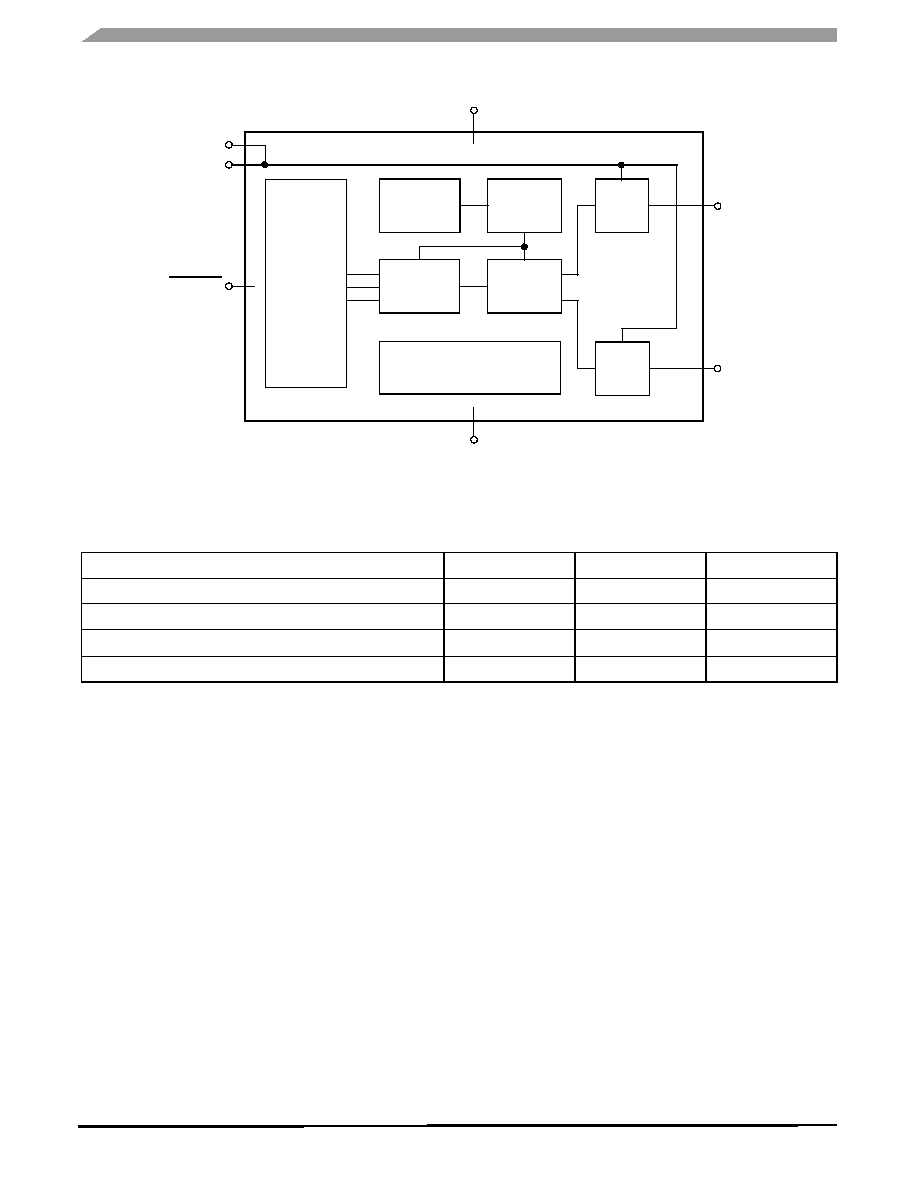
Figure 2. Simplified Accelerometer Functional Block Diagram
ELECTRO STATIC DISCHARGE (ESD)
WARNING: This device is sensitive to electrostatic
discharge.
Although the Freescale accelerometer contains internal
2000 V ESD protection circuitry, extra precaution must be
taken by the user to protect the chip from ESD. A charge of
over 2000 volts can accumulate on the human body or
associated test equipment. A charge of this magnitude can
alter the performance or cause failure of the chip. When
handling the accelerometer, proper ESD precautions should
be followed to avoid exposing the device to discharges which
may be detrimental to its performance.
Table 1. Maximum Ratings
(Maximum ratings are the limits to which the device can be exposed without causing permanent damage.)
Rating
Symbol
Value
Unit
Maximum Acceleration (all axis)
g
max
±2000
g
Supply Voltage
V
DD
≠0.3 to +3.6
V
Drop Test
(1)
1. Dropped onto concrete surface from any axis.
D
drop
1.8
m
Storage Temperature Range
T
stg
≠40 to +125
∞
C
V
SS
Y
OUT
X
OUT
g-Select1
g-Select2
Sleep Mode
V
DD
G-Cell
Sensor
Oscillator
Clock
Generator
X-Temp
Comp
Y-Temp
Comp
C to V
Converter
Gain
+
Filter
Control Logic
EEPROM Trim Circuits
Analog Integrated Circuit Device Data
Freescale Semiconductor
3
MMA6270Q
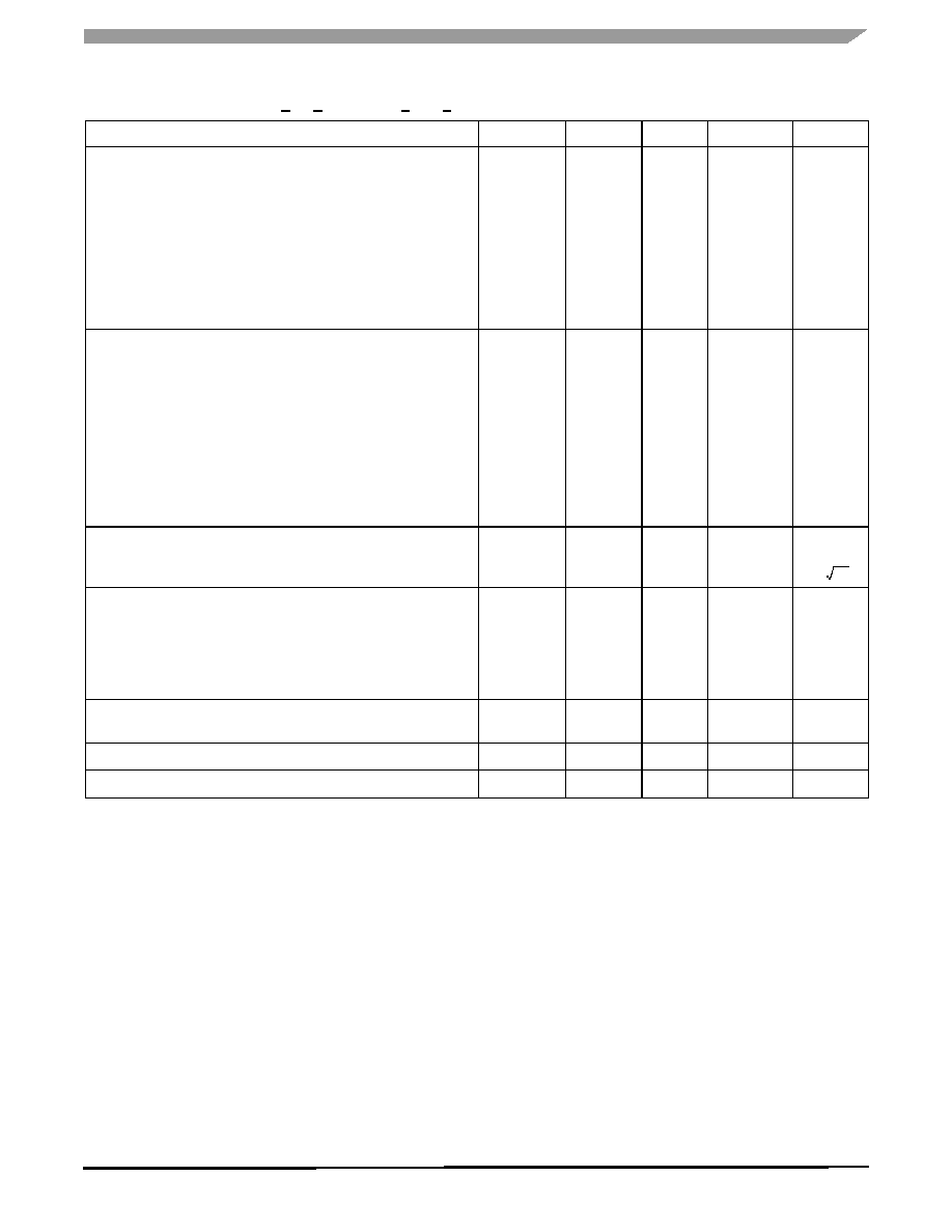
Table 2. Operating Characteristics
Unless otherwise noted: ≠20∞C < T
A
< 85∞C, 2.2 V < V
DD
< 3.6 V, Acceleration = 0 g, Loaded output
(1)
Characteristic
Symbol
Min
Typ
Max
Unit
Operating Range
(2)
Supply Voltage
(3)
Supply Current
Supply Current at Sleep Mode
(4)
Operating Temperature Range
Acceleration Range, X-Axis, Y-Axis,
g-Select1 & 2: 00
g-Select1 & 2: 10
g-Select1 & 2: 01
g-Select1 & 2: 11
V
DD
I
DD
I
DD
T
A
g
FS
g
FS
g
FS
g
FS
2.2
--
--
≠20
--
--
--
--
3.3
500
3
--
±1.5
±2.0
±4.0
±6.0
3.6
800
10
+85
--
--
--
--
V
µ
A
µ
A
∞C
g
g
g
g
Output Signal
Zero g (T
A
= 25∞C, V
DD
= 3.3 V)
(5)
Zero g
Sensitivity (T
A
= 25∞C, V
DD
= 3.3 V)
1.5 g
2 g
4 g
6 g
Sensitivity
Bandwidth Response
XY
V
OFF
V
OFF
, T
A
S
1.5g
S
2g
S
4g
S
6g
S, T
A
f
-3dB
1.485
--
740
555
277.5
185
--
--
1.65
±2
800
600
300
200
±0.03
350
1.815
--
860
645
322.5
215
--
--
V
mg/∞C
mV/g
mV/g
mV/g
mV/g
%/∞C
Hz
Noise
RMS (0.1 Hz ≠ 1 kHz)
(4)
Power Spectral Density RMS (0.1 Hz ≠ 1 kHz)
(4)
n
RMS
n
PSD
--
--
4.7
350
--
--
mVrms
µ
g/
Control Timing
Power-Up Response Time
(6)
Enable Response Time
(7)
Sensing Element Resonant Frequency
XY
Internal Sampling Frequency
t
RESPONSE
t
ENABLE
f
GCELL
f
CLK
--
--
--
--
1.0
0.5
6.0
11
2.0
2.0
--
--
ms
ms
kHz
kHz
Output Stage Performance
Full-Scale Output Range (I
OUT
= 30 µA)
V
FSO
V
SS
+0.25
--
V
DD
≠0.25
V
Nonlinearity, X
OUT
, Y
OUT
NL
OUT
≠1.0
--
+1.0
%FSO
Cross-Axis Sensitivity
(8)
V
XY, XZ, YZ
--
--
5.0
%
1. For a loaded output, the measurements are observed after an RC filter consisting of a 1.0 k
resistor and a 0.1 µF capacitor on V
DD
-GND.
2. These limits define the range of operation for which the part will meet specification.
3. Within the supply range of 2.2 and 3.6 V, the device operates as a fully calibrated linear accelerometer. Beyond these supply limits the device
may operate as a linear device but is not guaranteed to be in calibration.
4. This value is measured with g-Select in 1.5 g mode.
5. The device can measure both + and ≠ acceleration. With no input acceleration the output is at midsupply. For positive acceleration the output
will increase above V
DD
/2. For negative acceleration, the output will decrease below V
DD
/2.
6. The response time between 10% of full scale Vdd input voltage and 90% of the final operating output voltage.
7. The response time between 10% of full scale Sleep Mode input voltage and 90% of the final operating output voltage.
8. A measure of the device's ability to reject an acceleration applied 90∞ from the true axis of sensitivity.
Hz
Analog Integrated Circuit Device Data
4
Freescale Semiconductor
MMA6270Q
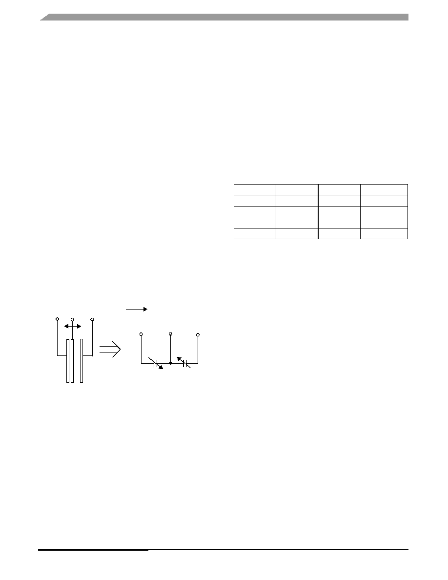
PRINCIPLE OF OPERATION
The Freescale accelerometer is a surface-micromachined
integrated-circuit accelerometer.
The device consists of two surface micromachined
capacitive sensing cells (g-cell) and a signal conditioning
ASIC contained in a single integrated circuit package. The
sensing elements are sealed hermetically at the wafer level
using a bulk micromachined cap wafer.
The g-cell is a mechanical structure formed from
semiconductor materials (polysilicon) using semiconductor
processes (masking and etching). It can be modeled as a set
of beams attached to a movable central mass that move
between fixed beams. The movable beams can be deflected
from their rest position by subjecting the system to an
acceleration (
Figure 3
).
As the beams attached to the central mass move, the
distance from them to the fixed beams on one side will
increase by the same amount that the distance to the fixed
beams on the other side decreases. The change in distance
is a measure of acceleration.
The g-cell beams form two back-to-back capacitors
(
Figure 3
). As the center beam moves with acceleration, the
distance between the beams changes and each capacitor's
value will change, (C = A
/D). Where A is the area of the
beam,
is the dielectric constant, and D is the distance
between the beams.
The ASIC uses switched capacitor techniques to measure
the g-cell capacitors and extract the acceleration data from
the difference between the two capacitors. The ASIC also
signal conditions and filters (switched capacitor) the signal,
providing a high level output voltage that is ratiometric and
proportional to acceleration.
Figure 3. Simplified Transducer Physical Model
SPECIAL FEATURES
g-Select
The g-Select feature allows for the selection among 4
sensitivities present in the device. Depending on the logic
input placed on pins 1 and 2, the device internal gain will be
changed allowing it to function with a 1.5 g, 2 g, 4 g, or 6 g
sensitivity (
Table 3
). This feature is ideal when a product has
applications requiring different sensitivities for optimum
performance. The sensitivity can be changed at anytime
during the operation of the product. The g-Select1 and g-
Select2 pins can be left unconnected for applications
requiring only a 1.5 g sensitivity as the device has an internal
pull-down to keep it at that sensitivity (800 mV/g).
Sleep Mode
The dual axis accelerometer provides a Sleep Mode that
is ideal for battery operated products. When Sleep Mode is
active, the device outputs are turned off, providing significant
reduction of operating current. A low input signal on pin 12
(Sleep Mode) will place the device in this mode and reduce
the current to 3 uA typ. For lower power consumption, it is
recommended to set g-Select1 and g-Select2 to 1.5 g mode.
By placing a high input signal on pin 12, the device will
resume to normal mode of operation.
Filtering
The dual axis accelerometer contains onboard single-pole
switched capacitor filters. Because the filter is realized using
switched capacitor techniques, there is no requirement for
external passive components (resistors and capacitors) to set
the cut-off frequency.
Ratiometricity
Ratiometricity simply means the output offset voltage and
sensitivity will scale linearly with applied supply voltage. That
is, as supply voltage is increased, the sensitivity and offset
increase linearly; as supply voltage decreases, offset and
sensitivity decrease linearly. This is a key feature when
interfacing to a microcontroller or an A/D converter because
it provides system level cancellation of supply induced errors
in the analog to digital conversion process.
Acceleration
Table 3. g-Select Pin Descriptions
g-Select2
g-Select1
g-Range
Sensitivity
0
0
1.5 g
800 mV/g
0
1
2 g
600 mV/g
1
0
4 g
300 mV/g
1
1
6 g
200 mV/g
Analog Integrated Circuit Device Data
Freescale Semiconductor
5
MMA6270Q
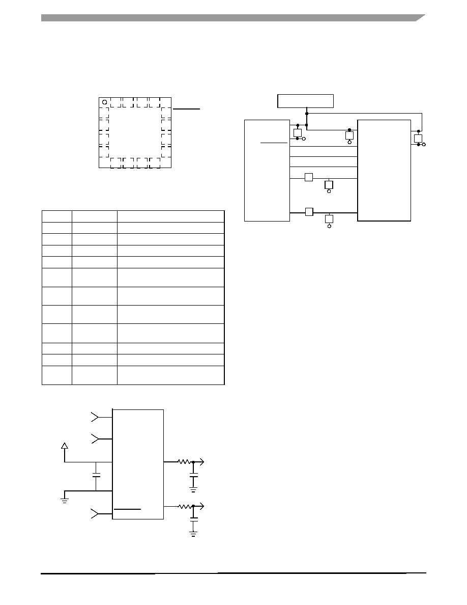
BASIC CONNECTIONS
Pin Descriptions
Figure 4. Pinout Description
Figure 5. Accelerometer with Recommended
Connection Diagram
PCB Layout
Figure 6. Recommended PCB Layout for Interfacing
Accelerometer to Microcontroller
NOTES:
1. Use 0.1 µF capacitor on V
DD
to decouple the power
source. Do not exceed capacitor values of 2.2 or
3.3 µF.
2. Physical coupling distance of the accelerometer to
the microcontroller should be minimal.
3. Flag underneath package is connected to ground.
4. Place a ground plane beneath the accelerometer to
reduce noise, the ground plane should be attached to
all of the open ended terminals shown in
Figure 6
.
5. Use an RC filter with 1.0 k
and 0.1 µF on the
outputs of the accelerometer to minimize clock noise
(from the switched capacitor filter circuit).
6. PCB layout of power and ground should not couple
power supply noise.
7. Accelerometer and microcontroller should not be a
high current path.
8. A/D sampling rate and any external power supply
switching frequency should be selected such that
they do not interfere with the internal accelerometer
sampling frequency (11 kHz for the sampling
frequency). This will prevent aliasing errors.
Table 4. Pin Descriptions
Pin No.
Pin Name
Description
1
g-Select1
Logic input pin to select g level.
2
g-Select2
Logic input pin to select g level.
3
V
DD
Power Supply Input
4
V
SS
Power Supply Ground
5 - 7
N/C
No internal connection.
Leave unconnected.
8 - 11
N/C
Unused for factory trim.
Leave unconnected.
12
Sleep Mode
Logic input pin to enable product or
Sleep Mode.
13
N/C
No internal connection.
Leave unconnected
14
Y
OUT
Y direction output voltage.
15
X
OUT
X direction output voltage.
16
N/C
No internal connection.
Leave unconnected.
Top View
15
16
14 13
12
11
10
1
2
3
4
5
6
7
8
9
g-Select1
NC
NC
NC
g-Select2
V
DD
V
SS
NC
NC
NC
NC
NC
NC
X
OUT
Y
OUT
Sleep Mode
Sleep Mode
V
DD
V
SS
0.1
µF
3
4
V
DD
0.1
µF
14
0.1
µF
15
12
X
OUT
Y
OUT
1 k
1 k
Logic
Input
2
1
Logic
Inputs
g-Select2
g-Select1
MMA6270Q
POWER SUPPLY
V
DD
V
SS
Sleep Mode
g-Select1
g-Select2
X
OUT
Y
OUT
Ac
cel
ero
m
ete
r
V
DD
V
SS
V
RH
P0
P1
P2
A/D
IN
A/D
IN
C
C
C
R
R
C
C
Mic
r
oc
ont
rol
l
e
r
C
C