MMG3007NT1
1
RF Device Data
Freescale Semiconductor
MMG3007NT1
0-6000 MHz, 19 dB
16 dBm
InGaP HBT
Heterojunction Bipolar Transistor
(InGaP HBT)
Broadband High Linearity Amplifier
The MMG3007NT1 is a General Purpose Amplifier that is internally
input and output matched. It is designed for a broad range of Class A,
small -signal, high linearity, general purpose applications. It is suitable
for applications with frequencies from 0 to 6000 MHz such as Cellular,
P C S , B WA , W L L , P H S , C AT V, V H F, U H F, U M T S a n d g e n e ra l
small-signal RF.
Features
∑ Frequency: 0 to 6000 MHz
∑ P1dB: 16 dBm @ 900 MHz
∑ Small-Signal Gain: 19 dB @ 900 MHz
∑ Third Order Output Intercept Point: 30 dBm @ 900 MHz
∑ Single 5 Volt Supply
∑ Internally Matched to 50 Ohms
∑ Low Cost SOT-89 Surface Mount Package
∑ Pb-Free and RoHS Compliant
∑ In Tape and Reel. T1 Suffix = 1000 Units per 12 mm, 7 inch Reel.
CASE 1514-01, STYLE 1
SOT-89
PLASTIC
1 2
3
Table 1. Typical Performance
(1)
Characteristic
Symbol
900
MHz
2140
MHz
3500
MHz
Unit
Small-Signal Gain
(S21)
G
p
19
16.5
14
dB
Input Return Loss
(S11)
IRL
-14
-21
-21
dB
Output Return Loss
(S22)
ORL
-20
-17
-25
dB
Power Output @1dB
Compression
P1db
16
15.5
16
dBm
Third Order Output
Intercept Point
IP3
30
29
28.5
dBm
1. V
CC
= 5 Vdc, T
C
= 25∞C, 50 ohm system
Table 2. Maximum Ratings
Rating
Symbol
Value
Unit
Supply Voltage
(2)
V
CC
7
V
Supply Current
(2)
I
CC
250
mA
RF Input Power
P
in
10
dBm
Storage Temperature Range
T
stg
-65 to +150
∞C
Junction Temperature
(3)
T
J
150
∞C
2. Continuous voltage and current applied to device.
3. For reliable operation, the junction temperature should not
exceed 150∞C.
Table 3. Thermal Characteristics
(V
CC
= 5 Vdc, I
CC
= 47 mA, T
C
= 25∞C)
Characteristic
Symbol
Value
(4)
Unit
Thermal Resistance, Junction to Case
R
JC
77
∞C/W
4. Refer to AN1955, Thermal Measurement Methodology of RF Power Amplifiers. Go to http://www.freescale.com/rf.
Select Documentation/Application Notes - AN1955.
Document Number: MMG3007NT1
Rev. 1, 8/2005
Freescale Semiconductor
Technical Data
Freescale Semiconductor, Inc., 2005. All rights reserved.

2
RF Device Data
Freescale Semiconductor
MMG3007NT1
Table 4. Electrical Characteristics
(V
CC
= 5 Vdc, 900 MHz, T
C
= 25∞C, 50 ohm system, in Freescale Application Circuit)
Characteristic
Symbol
Min
Typ
Max
Unit
Small-Signal Gain (S21)
G
p
18
19
--
dB
Input Return Loss (S11)
IRL
--
-14
--
dB
Output Return Loss (S22)
ORL
--
-20
--
dB
Power Output @ 1dB Compression
P1dB
--
16
--
dBm
Third Order Output Intercept Point
IP3
--
30
--
dBm
Noise Figure
NF
--
3.8
--
dB
Supply Current
(1)
I
CC
39
47
55
mA
Supply Voltage
(1)
V
CC
--
5
--
V
1. For reliable operation, the junction temperature should not exceed 150∞C.
MMG3007NT1
3
RF Device Data
Freescale Semiconductor
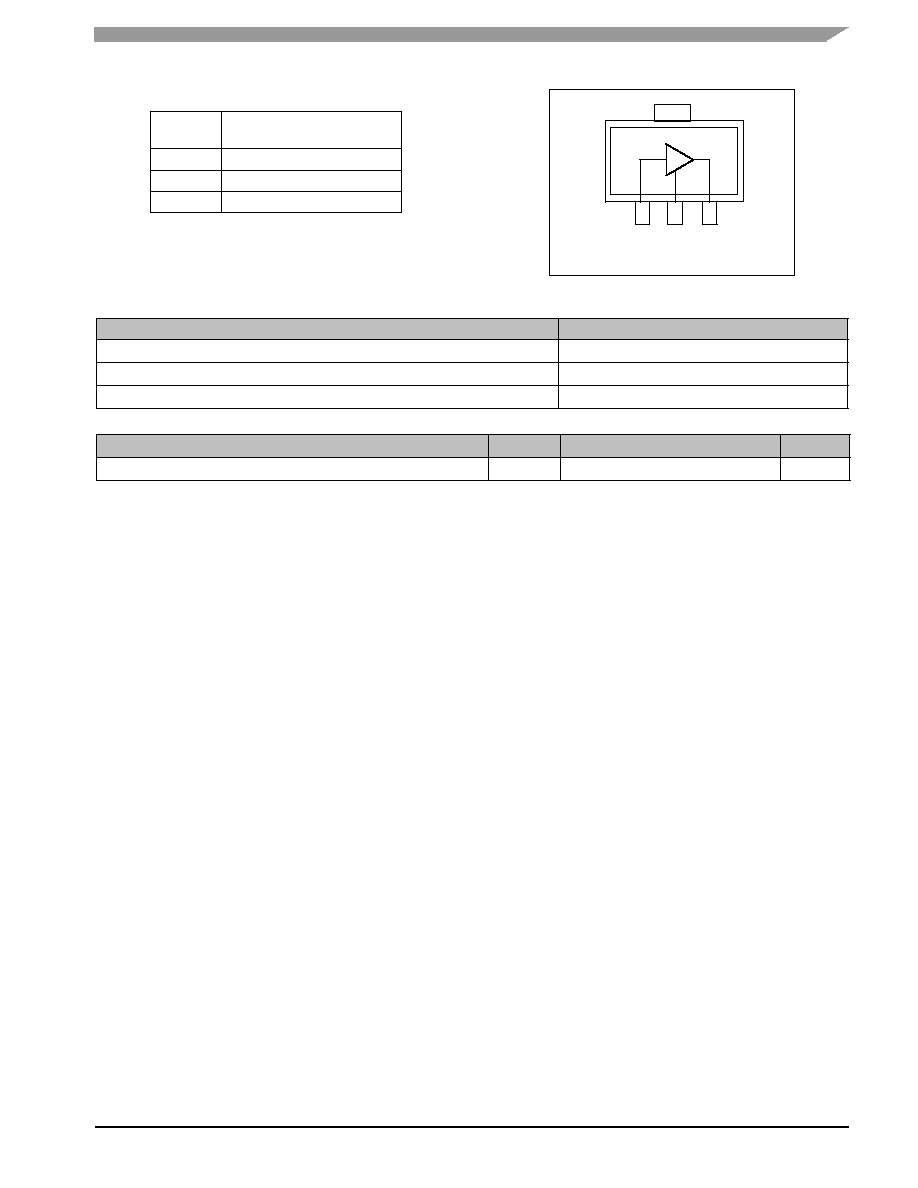
Table 5. Functional Pin Description
Pin
Number
Pin Function
1
RF
in
2
Ground
3
RF
out
/DC Supply
Table 6. ESD Protection Characteristics
Test Methodology
Class
Human Body Model (per JESD 22-A114)
1A (Minimum)
Machine Model (per EIA/JESD 22-A115)
A (Minimum)
Charge Device Model (per JESD 22-C101)
IV (Minimum)
Table 7. Moisture Sensitivity Level
Test Methodology
Rating
Package Peak Temperature
Unit
Per JESD 22-A113, IPC/JEDEC J-STD-020
1
260
∞C
Figure 1. Functional Diagram
3
2
1
2
4
RF Device Data
Freescale Semiconductor
MMG3007NT1
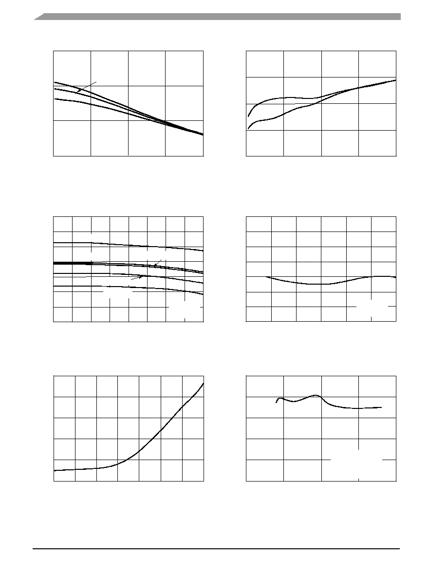
50 OHM TYPICAL CHARACTERISTICS
10
25
0
T
C
= 85
∞C
f, FREQUENCY (GHz)
Figure 2. Small-Signal Gain (S21) versus
Frequency
20
15
1
2
3
4
G
p
,
SMALL-SIGNAL GAIN (dB)
25
∞C
-40∞C
4
-40
0
0
S22
f, FREQUENCY (GHz)
Figure 3. Input/Output Return Loss versus
Frequency
V
CC
= 5 Vdc
I
CC
= 47 mA
S11
-10
-20
-30
1
2
3
S1
1, S22 (dB)
16
9
23
8
P
out
, OUTPUT POWER (dBm)
Figure 4. Small-Signal Gain versus Output
Power
V
CC
= 5 Vdc
I
CC
= 47 mA
21
19
17
15
13
9
10
12
1960 MHz
11
14
3.5
3
2.5
2
1.5
1
0.5
13
20
19
18
16
14
V
CC
= 5 Vdc
I
CC
= 47 mA
f, FREQUENCY (GHz)
Figure 5. P1dB versus Frequency
P1dB,
1 dB COMPRESSION POINT (dBm)
17
15
5.4
0
100
4
V
CC
, COLLECTOR VOLTAGE (V)
Figure 6. Collector Current versus Collector
Voltage
80
60
20
4.2
5
5.2
I
CC
,
COLLECTOR CURRENT (mA)
40
4.4
4.6
4.8
4
18
33
0
f, FREQUENCY (GHz)
Figure 7. Third Order Output Intercept Point
versus Frequency
30
27
24
21
1
2
3
V
CC
= 5 Vdc
I
CC
= 47 mA
1 MHz Tone Spacing
IP3, THIRD ORDER OUTPUT INTERCEPT POINT (dBm)
15
13
11
G
p
, SMALL-SIGNAL GAIN (dB)
V
CC
= 5 Vdc
900 MHz
2600 MHz
3500 MHz
2140 MHz
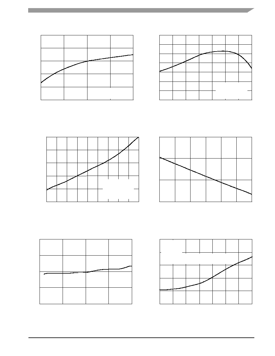
MMG3007NT1
5
RF Device Data
Freescale Semiconductor
50 OHM TYPICAL CHARACTERISTICS
21
36
4.9
V
CC
, COLLECTOR VOLTAGE (V)
Figure 8. Third Order Output Intercept Point
versus Collector Voltage
33
30
27
24
IP3,
THIRD ORDER OUTPUT INTERCEPT POINT (dBm)
4.95
5
5.1
5.05
f = 900 MHz
1 MHz Tone Spacing
100
-40
-20
0
20
40
60
80
25
32
T, TEMPERATURE (
_C)
Figure 9. Third Order Output Intercept Point
versus Case Temperature
30
29
28
27
IP3,
THIRD ORDER OUTPUT INTERCEPT POINT (dBm)
26
Figure 10. Third Order Intermodulation versus
Output Power
P
out
, OUTPUT POWER (dBm)
IMD, THIRD ORDER
INTERMODULA
TION
DISTORTION (dBc)
-3
1
5
9
13
-80
-30
-50
-60
-70
V
CC
= 5 Vdc
I
CC
= 47 mA
f = 900 MHz
1 MHz Tone Spacing
-40
150
10
3
10
6
120
Figure 11. MTTF versus Junction Temperature
10
4
125
130
135
140
145
T
J
, JUNCTION TEMPERATURE (
∞C)
NOTE: The MTTF is calculated with V
CC
= 5 Vdc, I
CC
= 47 mA
MTTF (YEARS)
4
0
8
0
f, FREQUENCY (GHz)
Figure 12. Noise Figure versus Frequency
V
CC
= 5 Vdc
I
CC
= 47 mA
6
4
2
1
2
3
NF
, NOISE FIGURE (dB)
-70
-20
-2
P
out
, OUTPUT POWER (dBm)
Figure 13. Single-Carrier W-CDMA Adjacent
Channel Power Ratio versus Output Power
-30
-40
-50
-60
8
6
4
0
ACPR,
ADJACENT CHANNEL POWER RA
TIO (dB)
10
12
31
10
5
2
V
CC
= 5 Vdc
f = 900 MHz
1 MHz Tone Spacing
V
CC
= 5 Vdc
I
CC
= 47 mA
f = 2140 MHz
Single-Carrier W-CDMA, 3.84 MHz Channel Bandwidth
PAR = 8.5 dB @ 0.01% Probability (CCDF)