Äîêóìåíòàöèÿ è îïèñàíèÿ www.docs.chipfind.ru
MOTOROLA
SEMICONDUCTOR TECHNICAL DATA
This document contains certain information on a new product.
Specifications and information herein are subject to change without notice.
© Motorola, Inc. 2004
Document order number: MPC17517
Rev 1.0, 03/2004
17517
Advance Information
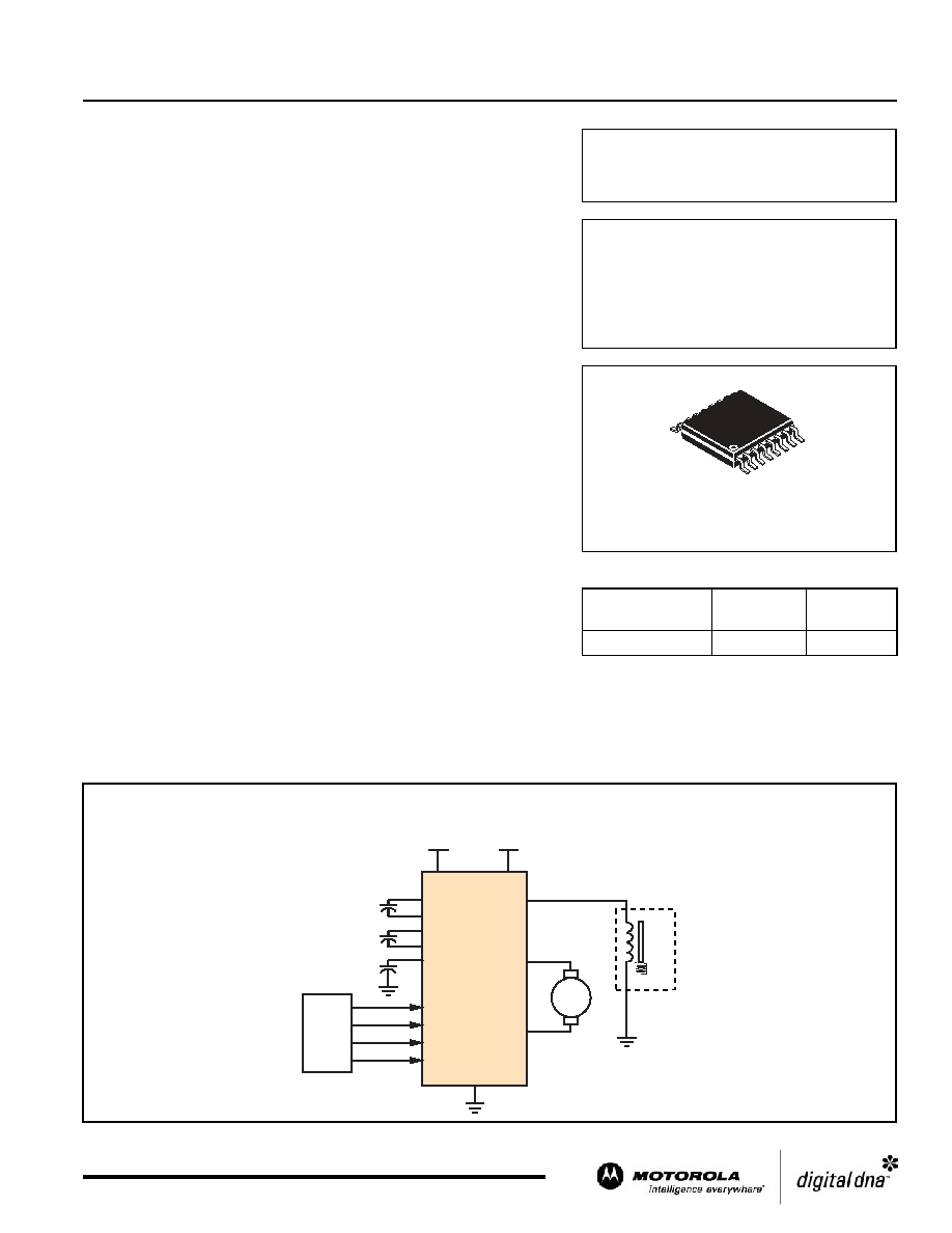
Simplified Application Diagram
V
DD
C
RES
C1L
C1H
C2L
C2H
IN2
IN1
EN1
OUTB
OUTA
OUTC
VM
GND
Solenoid
MCU
EN2
MOTOR
5.0 V
5.0 V
17517
17517 Simplified Application Diagram
1.0 A 6.8 V Dual Motor Driver IC
The 17517 is a monolithic triple totem-pole-output power IC designed to be
used in portable electronic applications to control small DC motors and
solenoids. The 17517 can operate efficiently with supply voltages as low as
2.0 V to as high as 6.8 V. Its low R
DS(ON)
totem-pole output MOSFETs (0.46
typical) can provide continuos drive currents of 1.0 A and handle peak currents
up to 3.0 A. It is easily interfaced to low-cost MCUs via parallel 3.0 V- or 5.0 V-
compatible logic. The device can be pulse width modulated (PWM-ed) at up to
200 kHz.
The 17517 can drive two motors in two directions one at a time or drive one
motor in two directions and one solenoid with synchronous rectification of
freewheeling currents one at a time. Two-motor operation is accomplished by
hooking one motor between OUTA and OUTB and hooking the other motor
between OUTB and OUTC. Motor plus solenoid operation is accomplished by
hooking a motor between OUTA and OUTB and a solenoid between OUTC
and GND.
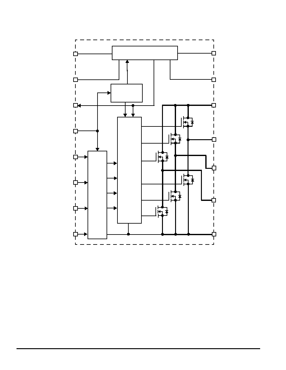
This device contains an integrated charge pump and level shifter (for gate
drive voltages), integrated shoot-through current protection (cross-conduction
suppression logic and timing), and undervoltage detection and shutdown
circuitry.
The 17517 has four operating modes: Forward, Reverse, Brake, and
Tri-Stated (High Impedance).
Features
· 2.0 V to 6.8 V Continuous Operation
· Output Current 1.0 A (DC), 3.0 A (Peak)
· MOSFETs < 600 m
R
DS(ON)
@ 25
°C Guaranteed
· 3.0 V/5.0 V TTL-/CMOS-Compatible Inputs
· PWM Frequencies up to 200 kHz
· Undervoltage Shutdown
ORDERING INFORMATION
Device
Temperature
Range (T
A
)
Package
MPC17517DTB/R2
-20°C to 65°C
16 TSSOP
DTB SUFFIX
CASE 948F-01
16-LEAD TSSOP
1.0 A 6.8 V DUAL MOTOR
DRIVER IC
F
r
e
e
s
c
a
l
e
S
e
m
i
c
o
n
d
u
c
t
o
r
,
I
Freescale Semiconductor, Inc.
For More Information On This Product,
Go to: www.freescale.com
n
c
.
.
.
17517
MOTOROLA ANALOG INTEGRATED CIRCUIT DEVICE DATA
2
Figure 1. 17517 Simplified Internal Block Diagram
Charge Pump
OUTA
GND
OUTB
OUTC
VM
C1L
C2H
C2L
C1H
C
RES
V
DD
IN1
IN2
EN1
EN2
Low-
Voltage
Shutdown
Control
Logic
Level
Shifter
Predriver
F
r
e
e
s
c
a
l
e
S
e
m
i
c
o
n
d
u
c
t
o
r
,
I
Freescale Semiconductor, Inc.
For More Information On This Product,
Go to: www.freescale.com
n
c
.
.
.
MOTOROLA ANALOG INTEGRATED CIRCUIT DEVICE DATA
17517
3
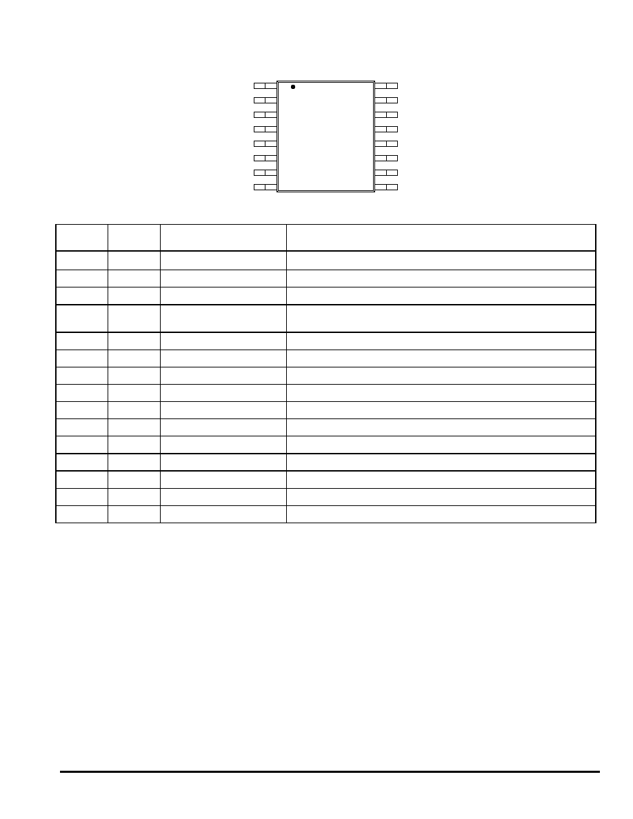
TERMINAL FUNCTION DESCRIPTION
Terminal
Terminal
Name
Formal Name
Definition
1
V
DD
Control Circuit Power Supply
Positive power source connection for control circuit.
2, 13
VM
Motor Drive Power Supply
Motor power supply voltage input terminals.
3
OUTA
Output A
Driver output A terminal.
4
C
RES
Charge Pump Output Capacitor
Connection
Charge pump reservoir capacitor terminal.
5
C2H
Charge Pump 2H
Charge pump bucket capacitor 2 (positive pole).
6
C2L
Charge Pump 2L
Charge pump bucket capacitor 2 (negative pole).
7
IN1
Input Control 1
Control signal input 1 terminal.
8
IN2
Input Control 2
Control signal input 2 terminal.
9
EN1
Enable Control Signal Input 1
Enable control signal input 1 terminal.
10
EN2
Enable Control Signal Input 2
Enable control signal input 2 terminal.
11
C1L
Charge Pump 1L
Charge pump bucket capacitor 1 (negative pole).
12
C1H
Charge Pump 1H
Charge pump bucket capacitor 1 (positive pole).
14
OUTB
Output B
Driver output B terminal.
15
GND
Ground
Ground connection.
16
OUTC
Output C
Driver output C terminal.
EN1
OUTC
GND
OUTB
VM
C1H
EN2
C1L
IN2
V
DD
VM
OUTA
C
RES
C2H
IN1
C2L
8
2
3
4
5
7
6
9
16
15
14
13
12
10
11
1
F
r
e
e
s
c
a
l
e
S
e
m
i
c
o
n
d
u
c
t
o
r
,
I
Freescale Semiconductor, Inc.
For More Information On This Product,
Go to: www.freescale.com
n
c
.
.
.
17517
MOTOROLA ANALOG INTEGRATED CIRCUIT DEVICE DATA
4
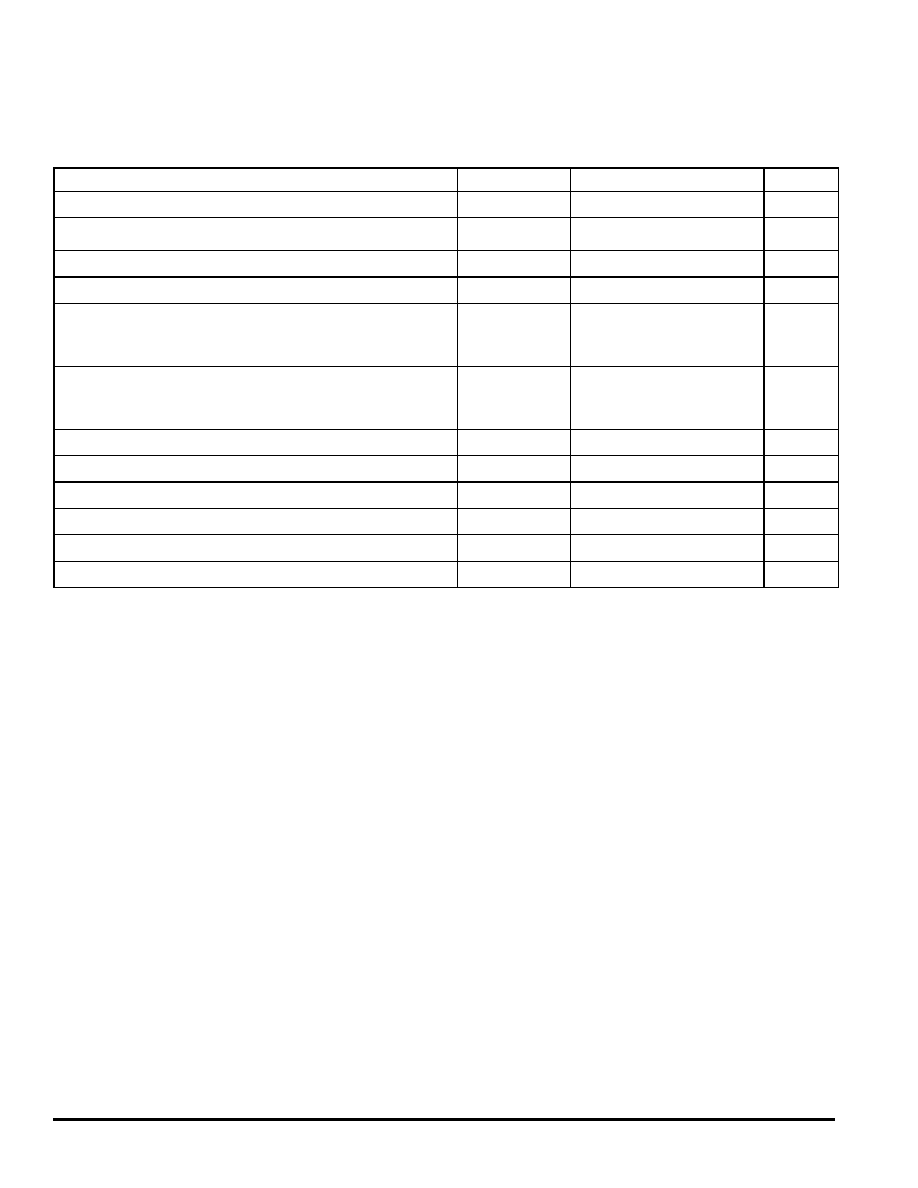
MAXIMUM RATINGS
All voltages are with respect to ground unless otherwise noted. Exceeding the ratings may cause a malfunction or permanent
damage to the device.
Rating
Symbol
Value
Unit
Motor Supply Voltage
V
M
-0.5 to 8.0
V
Charge Pump Output Voltage
V
C
RES
-0.5 to 14
V
Logic Supply Voltage
V
DD
-0.5 to 7.0
V
Signal Input Voltage
V
IN
-0.5 to V
DD
+0.5
V
Driver Output Current
Continuous
Peak (Note 1)
I
O
I
OPK
1.0
3.0
A
ESD Voltage
Human Body Model (Note 2)
Machine Model (Note 3)
V
ESD1
V
ESD2
±2000
±100
V
Storage Temperature Range
T
STG
-65 to 150
°C
Operating Junction Temperature
T
J
-20 to 150
°C
Operating Ambient Temperature
T
A
-20 to 65
°C
Thermal Resistance (Note 4)
R
JA
190
°C/W
Power Dissipation (Note 5)
P
D
657
mW
Soldering Temperature (Note 6)
T
SOLDER
245
°C
Notes
1.
T
A
= 25
°C, 10 ms pulse width at 200 ms intervals.
2.
ESD1 testing is performed in accordance with the Human Body Model (C
ZAP
= 100 pF, R
ZAP
= 1500
).
3.
ESD2 testing is performed in accordance with the Machine Model (C
ZAP
= 200 pF, R
ZAP
= 0
).
4.
37 mm x 50 mm Cu area (1.6 mm FR-4 PCB).
5.
Maximum at T
A
= 25
°C.
6.
Soldering temperature limit is for 10 seconds maximum duration. Not designed for immersion soldering. Exceeding these limits may cause
malfunction or permanent damage to the device.
F
r
e
e
s
c
a
l
e
S
e
m
i
c
o
n
d
u
c
t
o
r
,
I
Freescale Semiconductor, Inc.
For More Information On This Product,
Go to: www.freescale.com
n
c
.
.
.
MOTOROLA ANALOG INTEGRATED CIRCUIT DEVICE DATA
17517
5
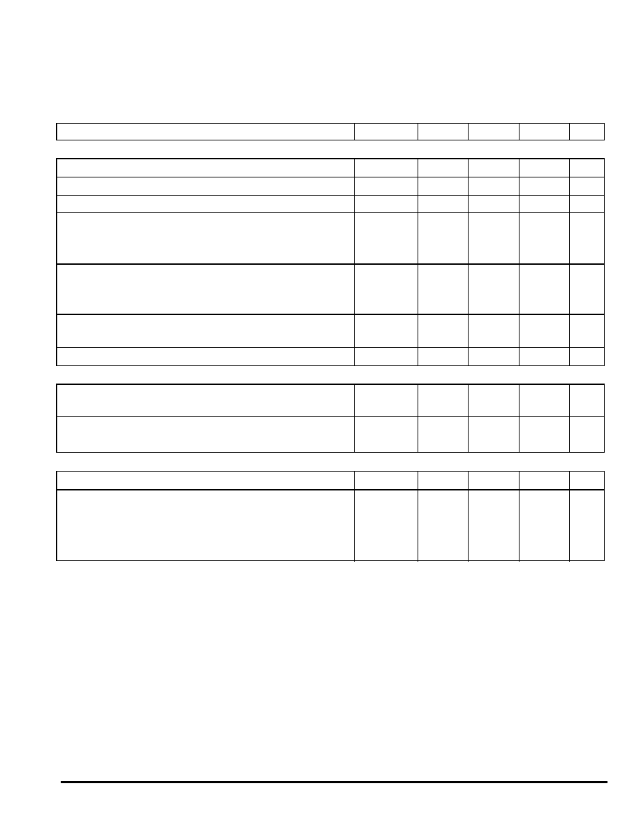
STATIC ELECTRICAL CHARACTERISTICS
Characteristics noted under conditions T
A
= 25
°C, V
DD
= V
M
= 5.0 V, GND = 0 V unless otherwise noted. Typical values noted reflect
the approximate parameter means at T
A
= 25
°C under nominal conditions unless otherwise noted.
Characteristic
Symbol
Min
Typ
Max
Unit
POWER
Motor Supply Voltage
V
M
2.0
5.0
6.8
V
Logic Supply Voltage
V
DD
2.7
5.0
5.7
V
Capacitor for Charge Pump
C1, C2, C3
0.01
0.1
1.0
µF
Standby Power Supply Current
Motor Supply Standby Current
Logic Supply Standby Current (Note 7)
IV
MSTBY
IV
DDSTBY
1.0
1.0
µA
mA
Operating Power Supply Current
Logic Supply Current (Note 8)
Charge Pump Circuit Supply Current
IV
DD
IC
RES
3.0
0.7
mA
Low-Voltage Detection Circuit
Detection Voltage (V
DD
) (Note 9)
V
DD
DET
1.5
2.0
2.5
V
Driver Output ON Resistance (Note 10)
R
DS(ON)
0.46
0.60
GATE DRIVE
Gate Drive Voltage (Note 11)
No Current Load
V
C
RES
12
13
13.5
V
Gate Drive Ability (Internally Supplied)
IC
RES
= -1.0 mA
VC
RES
load
10
11.2
V
CONTROL LOGIC
Logic Input Voltage
V
IN
0
V
DD
V
Logic Input Function (2.7 V < V
DD
< 5.7 V)
High-Level Input Voltage
Low-Level Input Voltage
High-Level Input Current
Low-Level Input Current
V
IH
V
IL
I
IH
I
IL
V
DD
x0.7
-1.0
V
DD
x0.3
1.0
V
V
µA
µA
Notes
7.
IV
DDSTBY
includes current to the predriver circuit.
8.
IV
DD
includes current to the predriver circuit.
9.
Detection voltage is defined as when the output becomes high-impedance after V
DD
drops below the detection threshold. When the gate
voltage VC
RES
is applied from an external source, VC
RES
= 7.5 V.
10.
I
O
= 1.0 A source + sink.
11.
Input logic signal not present.
F
r
e
e
s
c
a
l
e
S
e
m
i
c
o
n
d
u
c
t
o
r
,
I
Freescale Semiconductor, Inc.
For More Information On This Product,
Go to: www.freescale.com
n
c
.
.
.
Document Outline
- Introduction
- 17517 Simplified Application Diagram
- 17517 Simplified Internal Block Diagram
- Terminal Function Description
- Maximum Ratings
- Static Electrical Characteristics
- Dynamic Electrical Characteristics
- Timing Diagrams
- Truth Table
- System/Application Information
- Introduction
- Functional Terminal Description
- Applications
- Package Dimensions