Äîêóìåíòàöèÿ è îïèñàíèÿ www.docs.chipfind.ru

Freescale Semiconductor
Data Sheet: Product Preview
Document Number: MPC5534
Rev. 0, 06/2006
Contents
© Freescale Semiconductor, Inc., 2006. All rights reserved.
·
Preliminary--Subject to Change Without Notice
This document contains information on a new product. Specifications and information herein
are subject to change without notice.
This document provides electrical specifications, pin
assignments, and package diagrams for the MPC5534
microcontroller device. For functional characteristics,
refer to the MPC5534 Microcontroller Reference
Manual.
1
Overview
The MPC5534 microcontroller (MCU) is a member of
the MPC5500 family of microcontrollers based on the
PowerPCTM Book E architecture. This family of parts
contains many new features coupled with high
performance CMOS technology to provide substantial
reduction of cost per feature and significant performance
improvement over the MPC500 family.
The host processor core of this device is compatible with
the PowerPC Book E architecture. It is 100% user mode
compatible (with floating point library) with the classic
PowerPC instruction set. The Book E architecture has
enhancements that improve the PowerPC architecture's
fit in embedded applications. This core also has
additional instructions, including digital signal
processing (DSP) instructions, beyond the classic
1
Overview . . . . . . . . . . . . . . . . . . . . . . . . . . . . . . . . . . . . . 1
2
Ordering Information . . . . . . . . . . . . . . . . . . . . . . . . . . . . 3
3
Electrical Characteristics . . . . . . . . . . . . . . . . . . . . . . . . . 4
3.1
Maximum Ratings . . . . . . . . . . . . . . . . . . . . . . . . . . 4
3.2
Thermal Characteristics. . . . . . . . . . . . . . . . . . . . . . 5
3.3
Package . . . . . . . . . . . . . . . . . . . . . . . . . . . . . . . . . 8
3.4
EMI (Electromagnetic Interference) Characteristics 8
3.5
ESD Characteristics . . . . . . . . . . . . . . . . . . . . . . . . 9
3.6
VRC/POR Electrical Specifications . . . . . . . . . . . . . 9
3.7
Power Up/Down Sequencing. . . . . . . . . . . . . . . . . 10
3.8
DC Electrical Specifications. . . . . . . . . . . . . . . . . . 12
3.9
Oscillator & FMPLL Electrical Characteristics . . . . 19
3.10 eQADC Electrical Characteristics . . . . . . . . . . . . . 20
3.11 H7Fb Flash Memory Electrical Characteristics . . . 22
3.12 AC Specifications . . . . . . . . . . . . . . . . . . . . . . . . . 23
3.13 AC Timing . . . . . . . . . . . . . . . . . . . . . . . . . . . . . . . 25
4
Mechanicals. . . . . . . . . . . . . . . . . . . . . . . . . . . . . . . . . . 45
4.1
Pinouts . . . . . . . . . . . . . . . . . . . . . . . . . . . . . . . . . 45
4.2
Package Dimensions. . . . . . . . . . . . . . . . . . . . . . . 46
5
Revision History. . . . . . . . . . . . . . . . . . . . . . . . . . . . . . . 49
MPC5534 Microcontroller
Data Sheet
by: Microcontroller Division

MPC5534 Microcontroller Data Sheet, Rev. 0
Preliminary--Subject to Change Without Notice
Overview
Freescale Semiconductor
2
PowerPC instruction set. This family of parts contains many new features coupled with high performance
CMOS technology to provide significant performance improvement over the MPC565.
The host processor core of the MPC5534 also includes an instruction set enhancement allowing variable
length encoding (VLE). This allows optional encoding of mixed 16- and 32-bit instructions. With this
enhancement, it is possible to achieve significant code size footprint reduction.
The MPC5534 has a single level of memory hierarchy consisting of 64-Kbyte on-chip SRAM and 1 Mbyte
of internal Flash memory. Both the SRAM and the Flash memory can hold instructions and data. The
External Bus Interface has been designed to support most of the standard memories used with the MPC5xx
family. The MPC5534 does not support arbitration between itself and other masters on the external bus. It
must be either the only master on the external bus or act as a slave-only device.
The complex I/O timer functions of the MPC5534 are performed by an Enhanced Time Processor Unit
engine (eTPU). The eTPU engine controls 32 hardware channels. The eTPU has been enhanced over the
MPC500 family's TPU by providing 24-bit timers, double action hardware channels, variable number of
parameters per channel, angle clock hardware, and additional control and arithmetic instructions. The
eTPU can be programmed using a high-level programming language.
The less complex timer functions of MPC5534 are performed by the enhanced Modular Timer System
(eMIOS). The eMIOS 24 hardware channels are capable of single action, double action, pulse width
modulation (PWM) and modulus counter operation. Motor control capabilities include edge-aligned and
center-aligned PWM.
Off-chip communication is performed by a suite of serial protocols including CANs, enhanced SPIs
(Deserialize/Serialize Peripheral Interface) and SCIs. The DSPIs support pin reduction through hardware
serialization and deserialization of timer channels and GPIO signals.
The MPC5534 MCU has an on-chip 40-channel Enhanced Queued Dual Analog-to-Digital Converter
(eQADC)
,
with 5V conversion range.
The System Integration Unit (SIU) performs several chip-wide configuration functions. Pad configuration
and General-Purpose Input and Output (GPIO) are controlled from the SIU. External interrupts and reset
control are also found in the SIU. The Internal Multiplexer sub-block (IMUX) provides multiplexing of
eQADC trigger sources, daisy chaining the DSPIs and external interrupt signal multiplexing.
Ordering Information
MPC5534 Microcontroller Data Sheet, Rev. 0
Preliminary--Subject to Change Without Notice
Freescale Semiconductor
3
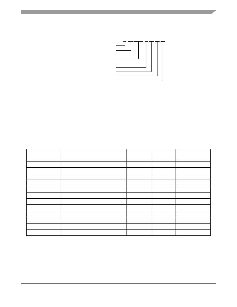
2
Ordering Information
Figure 1. MPC5500 Family Part Number Example
Table 1. Orderable Part Numbers
Freescale Part
Number
1
1
All devices are PPC5534, rather than MPC5534, until the product qualifications. Not all configurations will be available
in the PPC parts.
Description
Speed
(MHz)
Max Speed
2
(MHz) (f
MAX
)
2
Speed is the nominal maximum frequency. Max Speed is the maximum speed allowed including any frequency
modulation.
Temperature
MPC5534MVZ80
MPC5534 Lead free 324 package
80
80
-40° C to 125° C
MPC5534MZQ80
MPC5534 Lead 324 package
80
80
-40° C to 125° C
MPC5534MVM80
MPC5534 Lead free 208 package
80
80
-40° C to 125° C
MPC5534MVF80
MPC5534 Lead 208 package
80
80
-40° C to 125° C
MPC5534MVZ66
MPC5534 Lead free 324 package
66
66
-40° C to 125° C
MPC5534MZQ66
MPC5534 Lead 324 package
66
66
-40° C to 125° C
MPC5534MVM66
MPC5534 Lead free 208 package
66
66
-40° C to 125° C
MPC5534MVF66
MPC5534 Lead 208 package
66
66
-40° C to 125° C
MPC5534MVZ40
MPC5534 Lead free 324 package
40
40
-40° C to 125° C
MPC5534MZQ40
MPC5534 Lead 324 package
40
40
-40° C to 125° C
MPC5534MVM40
MPC5534 Lead free 208 package
40
40
-40° C to 125° C
MPC5534MVF40
MPC5534 Lead 208 package
40
40
-40° C to 125° C
M PC
M
80 R2
Qualification Status
Core Code
Device Number
Temperature Range
Package Identifier
Operating Frequency (MHz)
Tape and Reel Status
Temperature Range
M = -40° C to 125° C
A = -55° C to 125° C
Package Identifier
VF = 208MAPBGA SnPb
VM = 208MAPBGA Pb-free
ZQ = 324PBGA SnPb
VZ = 324PBGA Pb-free
Operating Frequency
40 = 40MHz
66 = 66MHz
80 = 80MHz
Note: Not all options are available on all devices. Refer to
Table 1
.
Tape and Reel Status
R2 = Tape and Reel
(blank) = Trays
Qualification Status
P = Pre Qualification
M = Full Spec Qualified
5534
ZQ
MPC5534 Microcontroller Data Sheet, Rev. 0
Preliminary--Subject to Change Without Notice
Electrical Characteristics
Freescale Semiconductor
4
3
Electrical Characteristics
This section contains detailed information on power considerations, DC/AC electrical characteristics, and
AC timing specifications for the MCU.
3.1
Maximum Ratings
Table 2. Absolute Maximum Ratings
1
Num
Characteristic
Symbol
Min
Max
2
Unit
1
1.5V Core Supply Voltage
3
V
DD
0.3
1.7
V
2
Flash Program/Erase Voltage
V
PP
0.3
6.5
V
3
Flash Core Voltage
V
DDF
0.3
1.7
V
4
Flash Read Voltage
V
FLASH
0.3
4.6
V
5
SRAM Standby Voltage
V
STBY
0.3
1.7
V
6
Clock Synthesizer Voltage
V
DDSYN
0.3
4.6
V
7
3.3V I/O Buffer Voltage
V
DD33
0.3
4.6
V
8
Voltage Regulator Control Input Voltage
V
RC33
0.3
4.6
V
9
Analog Supply Voltage (reference to V
SSA
)
V
DDA
0.3
5.5
V
10
I/O Supply Voltage (Fast I/O Pads)
4
V
DDE
0.3
4.6
V
11
I/O Supply Voltage (Slow/Medium I/O Pads)
4
V
DDEH
0.3
6.5
V
12
DC Input Voltage
5
VDDEH powered I/O Pads, except eTPUB15 and
SINB (DSPI_B_SIN)
VDDEH powered I/O Pads (eTPUB15 and SINB)
VDDE powered I/O Pads
V
IN
1.0
6
0.3
7
1.0
6
6.5
8
6.5
8
4.6
9
V
13
Analog Reference High Voltage (reference to VRL)
V
RH
0.3
5.5
V
14
VSS Differential Voltage
V
SS
V
SSA
0.1
0.1
V
15
VDD Differential Voltage
V
DD
V
DDA
V
DDA
V
DD
V
16
V
REF
Differential Voltage
V
RH
V
RL
0.3
5.5
V
17
V
RH
to VDDA Differential Voltage
V
RH
V
DDA
5.5
5.5
V
18
V
RL
to VSSA Differential Voltage
V
RL
V
SSA
0.3
0.3
V
19
V
DDEH
to V
DDA
Differential Voltage
V
DDEH
V
DDA
V
DDA
V
DDEH
V
20
V
DDF
to V
DD
Differential Voltage
V
DDF
V
DD
0.3
0.3
V
21
This spec has been moved to
Table 9
, spec 43a.
22
VSSSYN to VSS Differential Voltage
V
SSSYN
V
SS
0.1
0.1
V
23
V
RCVSS
to V
SS
Differential Voltage
V
RCVSS
V
SS
0.1
0.1
V
24
Maximum DC Digital Input Current
10
(per pin, applies to all
digital pins)
5
I
MAXD
2
2
mA
25
Maximum DC Analog Input Current
11
(per pin, applies to all
analog pins)
I
MAXA
3
3
mA
26
Maximum Operating Temperature Range
12
-- Die Junction
Temperature
T
J
40.0
150.0
o
C
Electrical Characteristics
MPC5534 Microcontroller Data Sheet, Rev. 0
Preliminary--Subject to Change Without Notice
Freescale Semiconductor
5
3.2
Thermal Characteristics
27
Storage Temperature Range
T
STG
55.0
150.0
o
C
28
Maximum Solder Temperature
13
T
SDR
--
260.0
o
C
29
Moisture Sensitivity Level
14
MSL
--
3
1
Functional operating conditions are given in the DC electrical specifications. Absolute maximum ratings are stress ratings only,
and functional operation at the maxima is not guaranteed. Stress beyond the listed maxima may affect device reliability or
cause permanent damage to the device.
2
Absolute maximum voltages are currently maximum burn-in voltages. Absolute maximum specifications for device stress have
not yet been determined.
3
1.5V +/ 10% for proper operation. This parameter is specified at a maximum junction temperature of 150C.
4
All functional non-supply I/O pins are clamped to VSS and VDDE or VDDEH.
5
AC signal over and undershoot of the input voltages of up to +/ 2.0 volts is permitted for a cumulative duration of 60 hours
over the complete lifetime of the device (injection current does not need to be limited for this duration).
6
Internal structures will hold the voltage above 1.0 volt if the injection current limit of 2 mA is met.
7
Internal structures will not clamp to a safe voltage. External protection must be used to ensure that voltage on the pin stays
above 0.3 volts.
8
Internal structures hold the input voltage below this maximum voltage on all pads powered by VDDEH supplies, if the maximum
injection current specification is met (2 mA for all pins) and VDDEH is within Operating Voltage specifications.
9
Internal structures hold the input voltage below this maximum voltage on all pads powered by VDDE supplies, if the maximum
injection current specification is met (2 mA for all pins) and VDDE is within Operating Voltage specifications.
10
Total injection current for all pins (including both digital and analog) must not exceed 25mA.
11
Total injection current for all analog input pins must not exceed 15mA.
12
Lifetime operation at these specification limits is not guaranteed.
13
Solder profile per CDF-AEC-Q100.
14
Moisture sensitivity per JEDEC test method A112.
Table 3. Thermal Characteristics
Num
Characteristic
Symbol
Unit
Value
208 MAPBGA
324 PBGA
1
Junction to Ambient
1, 2
Natural Convection
(Single layer board)
R
JA
°C/W
42
34
2
Junction to Ambient
1, 3
Natural Convection
(Four layer board 2s2p)
R
JA
°C/W
26
23
3
Junction to Ambient
(@200 ft./min.,
Single layer board)
R
JMA
°C/W
34
28
4
Junction to Ambient
(@200 ft./min.,
Four layer board 2s2p)
R
JMA
°C/W
22
20
5
Junction to Board
4
(Four layer board 2s2p)
R
JB
°C/W
15
15
Table 2. Absolute Maximum Ratings
1
(continued)
Num
Characteristic
Symbol
Min
Max
2
Unit
Document Outline