 | ÐлекÑÑоннÑй компоненÑ: MPC7448 | СкаÑаÑÑ:  PDF PDF  ZIP ZIP |
Äîêóìåíòàöèÿ è îïèñàíèÿ www.docs.chipfind.ru

© Freescale Semiconductor, Inc., 2005, 2006. All rights reserved.
Freescale Semiconductor
Technical Data
This document is primarily concerned with the PowerPCTM
MPC7448. The MPC7448 is an implementation of the
PowerPCTM microprocessor family of reduced instruction set
computer (RISC) microprocessors built on Power
ArchitectureTM technology. This document describes pertinent
electrical and physical characteristics of the MPC7448. For
information regarding specific MPC7448 part numbers
covered by this document and part numbers covered by other
documents, refer to
Section 11, "Part Numbering and
Marking."
For functional characteristics of the processor, refer
to the MPC7450 RISC Microprocessor Family Reference
Manual.
To locate any published updates for this document, refer to the
website listed on the back cover of this document.
1
Overview
The MPC7448 is the sixth implementation of fourth-
generation (G4) microprocessors from Freescale. The
MPC7448 implements the full 32-bit PowerPC architecture
(which is part of the Power Architecture technology) and is
targeted at networking and computing systems applications.
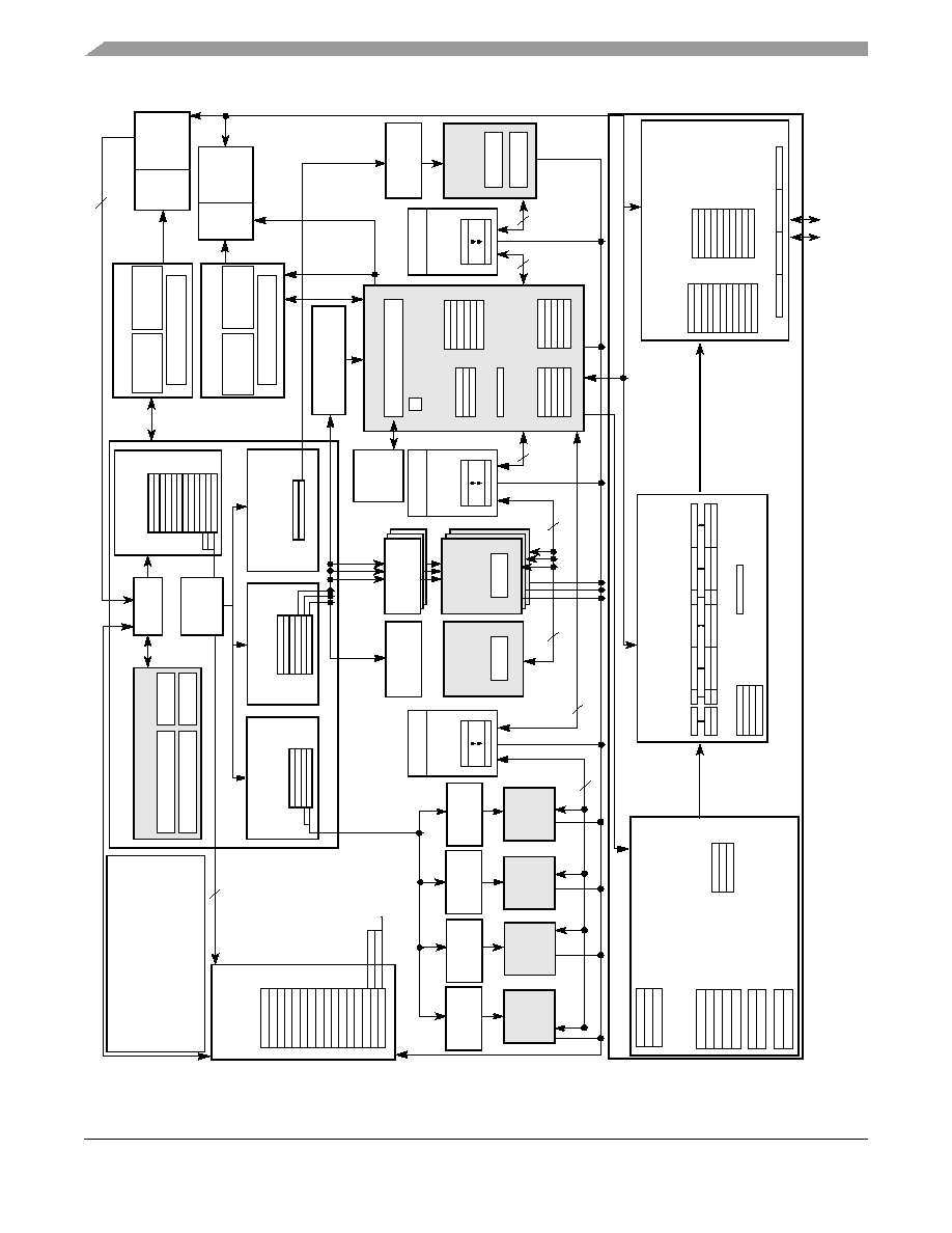
The MPC7448 consists of a processor core and a 1-Mbyte L2.
Figure 1
shows a block diagram of the MPC7448. The core is
a high-performance superscalar design supporting a
double-precision floating-point unit and a SIMD multimedia
unit. The memory storage subsystem supports the MPX bus
protocol and a subset of the 60x bus protocol to main memory
and other system resources.
Document Number: MPC7448EC
Rev. 3, 10/2006
Contents
1. Overview . . . . . . . . . . . . . . . . . . . . . . . . . . . . . . . . . . . 1
2. Features . . . . . . . . . . . . . . . . . . . . . . . . . . . . . . . . . . . . 3
3. Comparison with the MPC7447A, MPC7447,
MPC7445, and MPC7441 . . . . . . . . . . . . . . . . . . . . . . 7
4. General Parameters . . . . . . . . . . . . . . . . . . . . . . . . . . . 9
5. Electrical and Thermal Characteristics . . . . . . . . . . . . 9
6. Pin Assignments . . . . . . . . . . . . . . . . . . . . . . . . . . . . 23
7. Pinout Listings . . . . . . . . . . . . . . . . . . . . . . . . . . . . . 24
8. Package Description . . . . . . . . . . . . . . . . . . . . . . . . . 28
9. System Design Information . . . . . . . . . . . . . . . . . . . 34
10. Document Revision History . . . . . . . . . . . . . . . . . . . 56
11. Part Numbering and Marking . . . . . . . . . . . . . . . . . . 57
MPC7448
RISC Microprocessor
Hardware Specifications
MPC7448 RISC Microprocessor Hardware Specifications, Rev. 3
2
Freescale Semiconductor
Overview
Figure 1. MPC7448 Block Diagram
+
In
t
e
g
e
r
R
e
s
e
r
v
ati
on
St
a
t
i
o
n
Un
it
2
+
In
t
e
g
e
r
Re
s
e
r
v
a
t
i
o
n
St
a
t
i
o
n
Un
i
t
2
A
d
di
t
i
on
a
l
F
e
a
t
ur
e
s
· T
i
me B
a
s
e
C
ounte
r
/D
e
c
r
e
men
t
er
·
C
l
o
c
k M
u
lt
i
p
li
e
r
· J
T
A
G
/
C
O
P
Inter
f
ac
e
· T
h
e
r
mal
/
P
o
w
e
r
M
anage
ment
· P
e
r
f
or
ma
nc
e
Moni
tor
· O
u
t-
of-
O
r
d
er
Is
s
ue of
A
l
ti
V
e
c
Ins
t
r
.
+
+
x ÷
FP
S
C
R
FP
S
C
R
PA
+ x
÷
In
st
r
u
ct
io
n
Un
it
Ins
t
r
u
c
t
i
o
n Q
ueue
(
12-
W
o
r
d
)
96-
B
i
t (
3
Ins
t
r
u
c
t
i
o
ns
)
R
e
s
e
r
v
ati
on
In
t
e
g
e
r
1
28-
B
i
t
(
4
Ins
t
r
u
c
t
i
ons
)
32-
B
i
t
Fl
oa
ti
ng
-
Po
i
n
t
U
n
i
t
64
-
B
i
t
R
e
s
e
r
v
ati
on
Loa
d/
S
t
or
e
U
n
i
t
(
E
A
C
a
l
c
ul
a
t
i
on)
F
i
ni
s
hed
32
-
B
i
t
(
16-
E
n
t
r
y
)
T
ags
32-
K
b
y
t
e
D Ca
c
h
e
36
-
B
i
t
64-
B
i
t
In
t
e
g
e
r
S
t
ati
o
ns
(
2
)
R
e
s
e
r
v
ati
on
St
a
t
i
o
n
R
e
s
e
r
v
a
t
i
on
S
t
ati
ons
(
2
)
FP
R
Fi
l
e
16
R
enam
e
Bu
f
f
e
r
s
S
t
at
i
o
ns
(
2
-
E
n
t
r
y
)
GP
R
F
i
l
e
1
6
R
enam
e
Bu
f
f
e
r
s
Re
s
e
r
v
a
t
i
o
n
St
a
t
i
o
n
VR
F
i
le
16 R
e
name
Bu
f
f
e
r
s
64
-
B
i
t
128-
B
i
t
1
28-
B
i
t
C
o
m
p
l
e
ted
In
st
r
u
ct
io
n
MMU
SR
s
(
S
hadow
)
128-
E
n
tr
y
IB
A
T
A
r
r
a
y
IT
L
B
T
ags
32-
K
b
y
t
e
I Cac
h
e
S
t
or
es
S
t
or
es
Load Mi
s
s
Ve
c
t
o
r
To
u
c
h
Q
ueue
(3
)
V
R
Is
s
u
e
F
P
R
Is
s
u
e
B
r
an
ch
P
r
o
cessin
g
U
n
it
CT
R
LR
B
T
IC
(
128
-
E
ntr
y
)
B
H
T
(
2048
-
E
ntr
y
)
Fe
t
c
h
e
r
GP
R
I
ssu
e
(
6
-E
n
t
ry
/
3
-I
s
s
u
e
)
(4
-E
n
t
ry
/
2
-I
s
s
u
e
)
(2
-E
n
t
r
y
/
1
-
I
s
s
u
e
)
D
i
s
pat
c
h
Un
i
t
Da
t
a
M
M
U
SR
s
(
O
r
i
gi
nal
)
128
-
E
ntr
y
DB
A
T
A
r
r
a
y
DT
L
B
V
e
c
t
or
T
ouc
h E
ngi
ne
32-
B
i
t
EA
L1 C
a
s
t
out
S
t
atus
L
2
S
t
o
r
e
Q
u
eu
e (
L
2S
Q
)
V
ect
o
r
FP
U
R
e
s
e
r
v
ati
on
St
a
t
i
o
n
R
e
s
e
r
v
at
i
on
St
a
t
io
n
R
e
s
e
r
v
ati
on
St
a
t
io
n
Ve
c
t
o
r
In
t
e
g
e
r
Un
i
t
1
V
ect
o
r
In
t
e
g
e
r
Un
it
2
V
ect
o
r
Pe
rm
u
t
e
Un
it
Li
ne
Ta
g
s
B
l
o
ck 0 (
3
2
-
B
y
t
e
)
S
t
atus
B
l
o
c
k 1
(
32-
B
y
t
e
)
M
e
m
o
r
y
S
u
b
s
yst
em
S
noop P
u
s
h
/
Inte
r
v
ent
i
ons
L
1
C
a
st
o
u
t
s
Bu
s
Acc
u
mu
l
a
t
o
r
L1
P
u
s
h
(4
)
Un
it
2
U
n
i
t
1
L1 Lo
ad Q
u
e
ue (
LLQ
)
L1
Loa
d M
i
s
s
(
5
)
C
a
c
heab
le S
t
o
r
e
M
i
s
s
(
2
)
I
n
s
t
r
u
c
t
ion F
e
t
c
h (
2
)
L
1
S
e
r
v
ic
e
L1 S
t
or
e
Q
ueue
(L
S
Q
)
S
yst
e
m
B
u
s
I
n
t
e
r
f
a
c
e
L2
P
r
e
f
et
c
h
(
3
)
A
d
d
r
es
s
B
u
s
D
at
a B
u
s
Qu
e
u
e
s
Ca
st
o
u
t
Bus St
or
e Q
u
eue
Pu
sh
L
oad
Que
ue (
1
1)
Q
u
eu
e (5
) /
Que
ue (
6
)
1
Th
e Cas
t
ou
t
Queu
e a
nd P
u
sh
Queu
e s
har
e
r
e
s
our
c
e
s
su
ch
for
a
co
m
b
i
n
e
d
t
o
t
a
l
of
6
en
t
r
i
e
s.
Th
e Cas
t
ou
t
Queu
e i
t
se
l
f
i
s
l
i
m
i
t
e
d
t
o
5 en
t
r
i
e
s,
e
n
s
u
r
i
ng
1 e
n
t
r
y
wi
l
l
be
a
v
ai
l
abl
e
for
a pu
sh
.
1
-
M
b
yt
e U
n
if
ied
L
2
C
ach
e C
o
n
t
r
o
ller
N
o
t
es:
C
o
m
p
l
e
ti
on Q
ueu
e
Co
m
p
let
i
o
n
Un
it
Co
m
p
l
e
te
s
u
p
to th
r
e
e
per
c
l
oc
k
in
st
r
u
ct
i
o
n
s

MPC7448 RISC Microprocessor Hardware Specifications, Rev. 3
Freescale Semiconductor
3
Features
2
Features
This section summarizes features of the MPC7448 implementation.
Major features of the MPC7448 are as follows:
·
High-performance, superscalar microprocessor
-- Up to four instructions can be fetched from the instruction cache at a time.
-- Up to three instructions plus a branch instruction can be dispatched to the issue queues at a
time.
-- Up to 12 instructions can be in the instruction queue (IQ).
-- Up to 16 instructions can be at some stage of execution simultaneously.
-- Single-cycle execution for most instructions
-- One instruction per clock cycle throughput for most instructions
-- Seven-stage pipeline control
·
Eleven independent execution units and three register files
-- Branch processing unit (BPU) features static and dynamic branch prediction
128-entry (32-set, four-way set-associative) branch target instruction cache (BTIC), a cache
of branch instructions that have been encountered in branch/loop code sequences. If a target
instruction is in the BTIC, it is fetched into the instruction queue a cycle sooner than it can
be made available from the instruction cache. Typically, a fetch that hits the BTIC provides
the first four instructions in the target stream.
2048-entry branch history table (BHT) with 2 bits per entry for four levels of
prediction--not taken, strongly not taken, taken, and strongly taken
Up to three outstanding speculative branches
Branch instructions that do not update the count register (CTR) or link register (LR) are
often removed from the instruction stream.
Eight-entry link register stack to predict the target address of Branch Conditional to Link
Register (bclr) instructions
-- Four integer units (IUs) that share 32 GPRs for integer operands
Three identical IUs (IU1a, IU1b, and IU1c) can execute all integer instructions except
multiply, divide, and move to/from special-purpose register instructions.
IU2 executes miscellaneous instructions, including the CR logical operations, integer
multiplication and division instructions, and move to/from special-purpose register
instructions.
-- Five-stage FPU and 32-entry FPR file
Fully IEEE Std. 754TM-1985compliant FPU for both single- and double-precision
operations
Supports non-IEEE mode for time-critical operations
Hardware support for denormalized numbers
Thirty-two 64-bit FPRs for single- or double-precision operands
-- Four vector units and 32-entry vector register file (VRs)

MPC7448 RISC Microprocessor Hardware Specifications, Rev. 3
4
Freescale Semiconductor
Features
Vector permute unit (VPU)
Vector integer unit 1 (VIU1) handles short-latency AltiVecTM integer instructions, such as
vector add instructions (for example, vaddsbs, vaddshs, and vaddsws).
Vector integer unit 2 (VIU2) handles longer-latency AltiVec integer instructions, such as
vector multiply add instructions (for example, vmhaddshs, vmhraddshs, and
vmladduhm).
Vector floating-point unit (VFPU)
-- Three-stage load/store unit (LSU)
Supports integer, floating-point, and vector instruction load/store traffic
Four-entry vector touch queue (VTQ) supports all four architected AltiVec data stream
operations
Three-cycle GPR and AltiVec load latency (byte, half word, word, vector) with one-cycle
throughput
Four-cycle FPR load latency (single, double) with one-cycle throughput
No additional delay for misaligned access within double-word boundary
A dedicated adder calculates effective addresses (EAs).
Supports store gathering
Performs alignment, normalization, and precision conversion for floating-point data
Executes cache control and TLB instructions
Performs alignment, zero padding, and sign extension for integer data
Supports hits under misses (multiple outstanding misses)
Supports both big- and little-endian modes, including misaligned little-endian accesses
·
Three issue queues, FIQ, VIQ, and GIQ, can accept as many as one, two, and three instructions,
respectively, in a cycle. Instruction dispatch requires the following:
-- Instructions can only be dispatched from the three lowest IQ entries--IQ0, IQ1, and IQ2.
-- A maximum of three instructions can be dispatched to the issue queues per clock cycle.
-- Space must be available in the CQ for an instruction to dispatch (this includes instructions that
are assigned a space in the CQ but not in an issue queue).
·
Rename buffers
-- 16 GPR rename buffers
-- 16 FPR rename buffers
-- 16 VR rename buffers
·
Dispatch unit
-- Decode/dispatch stage fully decodes each instruction
·
Completion unit
-- Retires an instruction from the 16-entry completion queue (CQ) when all instructions ahead of
it have been completed, the instruction has finished executing, and no exceptions are pending
-- Guarantees sequential programming model (precise exception model)
-- Monitors all dispatched instructions and retires them in order

MPC7448 RISC Microprocessor Hardware Specifications, Rev. 3
Freescale Semiconductor
5
Features
-- Tracks unresolved branches and flushes instructions after a mispredicted branch
-- Retires as many as three instructions per clock cycle
·
Separate on-chip L1 instruction and data caches (Harvard architecture)
-- 32-Kbyte, eight-way set-associative instruction and data caches
-- Pseudo least-recently-used (PLRU) replacement algorithm
-- 32-byte (eight-word) L1 cache block
-- Physically indexed/physical tags
-- Cache write-back or write-through operation programmable on a per-page or per-block basis
-- Instruction cache can provide four instructions per clock cycle; data cache can provide four
words per clock cycle
-- Caches can be disabled in software.
-- Caches can be locked in software.
-- MESI data cache coherency maintained in hardware
-- Separate copy of data cache tags for efficient snooping
-- Parity support on cache
-- No snooping of instruction cache except for icbi instruction
-- Data cache supports AltiVec LRU and transient instructions
-- Critical double- and/or quad-word forwarding is performed as needed. Critical quad-word
forwarding is used for AltiVec loads and instruction fetches. Other accesses use critical
double-word forwarding.
·
Level 2 (L2) cache interface
-- On-chip, 1-Mbyte, eight-way set-associative unified instruction and data cache
-- Cache write-back or write-through operation programmable on a per-page or per-block basis
-- Parity support on cache tags
-- ECC or parity support on data
-- Error injection allows testing of error recovery software
·
Separate memory management units (MMUs) for instructions and data
-- 52-bit virtual address, 32- or 36-bit physical address
-- Address translation for 4-Kbyte pages, variable-sized blocks, and 256-Mbyte segments
-- Memory programmable as write-back/write-through, caching-inhibited/caching-allowed, and
memory coherency enforced/memory coherency not enforced on a page or block basis
-- Separate IBATs and DBATs (eight each) also defined as SPRs
-- Separate instruction and data translation lookaside buffers (TLBs)
Both TLBs are 128-entry, two-way set-associative and use an LRU replacement algorithm.
TLBs are hardware- or software-reloadable (that is, a page table search is performed in
hardware or by system software on a TLB miss).
·
Efficient data flow
-- Although the VR/LSU interface is 128 bits, the L1/L2 bus interface allows up to 256 bits.
Document Outline