 | –≠–ª–µ–∫—Ç—Ä–æ–Ω–Ω—ã–π –∫–æ–º–ø–æ–Ω–µ–Ω—Ç: MPC9239FA | –°–∫–∞—á–∞—Ç—å:  PDF PDF  ZIP ZIP |
MPC9239
Rev. 3, 08/2005
Freescale Semiconductor
Technical Data
© Freescale Semiconductor, Inc., 2005. All rights reserved.
900 MHz Low Voltage LVPECL
Clock Synthesizer
The MPC9239 is a 3.3 V compatible, PLL based clock synthesizer targeted for
high performance clock generation in mid-range to high-performance telecom,
networking, and computing applications. With output frequencies from
3.125 MHz to 900 MHz and the support of differential LVPECL output signals the
device meets the needs of the most demanding clock applications.
Features
∑
3.125 MHz to 900 MHz synthesized clock output signal
∑
Differential LVPECL output
∑
LVCMOS compatible control inputs
∑
On-chip crystal oscillator for reference frequency generation
∑
Alternative LVCMOS compatible reference input
∑
3.3 V power supply
∑
Fully integrated PLL
∑
Minimal frequency overshoot
∑
Serial 3-wire programming interface
∑
Parallel programming interface for power-up
∑
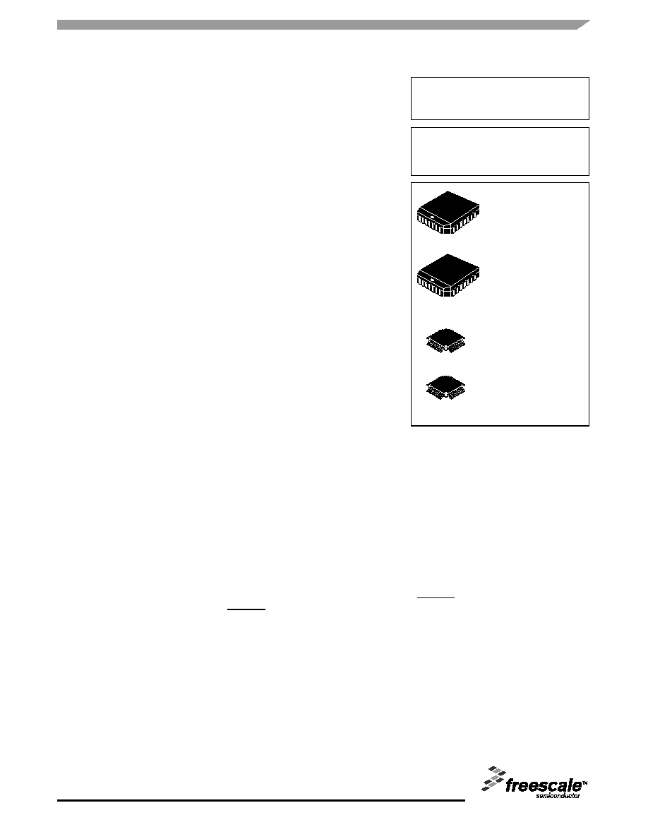
28 PLCC and 32 LQFP packaging
∑
28-lead and 32-lead Pb-free package available
∑
SiGe Technology
∑
Ambient temperature range 0
∞C to + 70∞C
∑
Pin and function compatible to the MC12439
Functional Description
The internal crystal oscillator uses the external quartz crystal as the basis of
its frequency reference. The frequency of the internal crystal oscillator or external
reference clock signal is multiplied by the PLL. The VCO within the PLL operates over a range of 800 to 1800 MHz. Its output is
scaled by a divider that is configured by either the serial or parallel interfaces. The crystal oscillator frequency f
XTAL
, the PLL
feedback-divider M and the PLL post-divider N determine the output frequency.
The feedback path of the PLL is internal. The PLL adjusts the VCO output frequency to be M times the reference frequency
by adjusting the VCO control voltage. Note that for some values of M (either too high or too low) the PLL will not achieve phase
lock. The PLL will be stable if the VCO frequency is within the specified VCO frequency range (800 to 1800 MHz). The M-value
must be programmed by the serial or parallel interface.
The PLL post-divider N is configured through either the serial or the parallel interfaces, and can provide one of four division
ratios (1, 2, 4, or 8). This divider extends performance of the part while providing a 50% duty cycle. The output driver is driven
differentially from the output divider, and is capable of driving a pair of transmission lines terminated 50
to V
CC
≠ 2.0 V. The
positive supply voltage for the internal PLL is separated from the power supply for the core logic and output drivers to minimize
noise induced jitter.
The configuration logic has two sections: serial and parallel. The parallel interface uses the values at the M[6:0] and N[1:0]
inputs to configure the internal counters. It is recommended on system reset to hold the P_LOAD input LOW until power becomes
valid. On the LOW-to-HIGH transition of P_LOAD, the parallel inputs are captured. The parallel interface has priority over the
serial interface. Internal pullup resistors are provided on the M[6:0] and N[1:0] inputs prevent the LVCMOS compatible control
inputs from floating. The serial interface centers on a twelve bit shift register. The shift register shifts once per rising edge of the
S_CLOCK input. The serial input S_DATA must meet setup and hold timing as specified in the AC Characteristics section of this
document. The configuration latches will capture the value of the shift register on the HIGH-to-LOW edge of the S_LOAD input.
Refer to the programming section for more information. The TEST output reflects various internal node values, and is controlled
by the T[2:0] bits in the serial data stream. In order to minimize the PLL jitter, it is recommended to avoid active signal on the
TEST output. The PWR_DOWN pin, when asserted, will synchronously divide the f
OUT
by 16. The power down sequence is
clocked by the PLL reference clock, thereby causing the frequency reduction to happen relatively slowly. Upon de-assertion of
the PWR_DOWN pin, the f
OUT
input will step back up to its programmed frequency in four discrete increments.
MPC9239
900 MHz LOW VOLTAGE
CLOCK SYNTHESIZER
FN SUFFIX
28-LEAD PLCC PACKAGE
CASE 776-02
FA SUFFIX
32-LEAD LQFP PACKAGE
CASE 873A-04
EI SUFFIX
28-LEAD PLCC PACKAGE
Pb-FREE PACKAGE
CASE 776-02
AC SUFFIX
32-LEAD LQFP PACKAGE
Pb-FREE PACKAGE
CASE 873A-04
Advanced Clock Drivers Devices
2
Freescale Semiconductor
MPC9239
Figure 1. MPC9239 Logic Diagram
Figure 2. MPC9239 28-Lead PLCC Pinout
(Top View)
Figure 3. MPC9239 32-Lead LQFP Pinout
(Top View)
XTAL_IN
XTAL_OUT
S_LOAD
S_DATA
S_CLOCK
M[0:6]
XTAL
11
00
01
10
M-LATCH
N-LATCH
10 ≠ 20 MHz
T-LATCH
2
TEST
3
LE
0
BITS 11-5
BITS 3-4
BITS 0-2
12-BIT SHIFT REGISTER
N[1:0]
OE
P/S
˜1
˜2
˜4
˜8
f
OUT
TEST
V
CC
V
CC
XTAL_SEL
f
REF_EXT
V
CC
1
0
˜16
1
0
PWR_DOWN
˜2
PLL
Ref
FB
VCO
800 ≠ 1800 MHz
˜0 TO ˜127
7-BIT M-DIVIDER
9
˜2
˜2
OE
1
0
1
P_LOAD
f
OUT
1
4
3
2
2
8
2
7
2
6
25
24
23
22
21
20
19
18
17
16
15
14
13
12
11
10
9
7
8
6
5
V
CC
XT
AL_OUT
P_L
O
AD
OE
M[0]
M[1]
M[2]
M[3]
f
OUT
f
OUT
GND
V
CC
T
EST
GND
S_CLOCK
N[1]
N[0]
NC
XTAL_SEL
M[6]
M[5]
M[4]
S_DATA
S_LOAD
V
CC_PLL
PWR_DOWN
f
REF_EXT
XTAL_IN
MPC9239
GND
TEST
V
CC
V
CC
GND
f
OUT
f
OUT
NC
M[3]
M[2]
M[1]
M[0]
P_LOAD
NC
N[1]
N[0]
NC
XT
AL_SEL
M[6]
M[5]
M[4]
S_CLOCK
S_LOAD
V
CC_PLL
V
CC_PLL
PWR_D
O
W
N
f
RE
F_
EXT
XTAL
_IN
25
26
27
28
29
30
31
32
15
14
13
12
11
10
9
1
2
3
4
5
6
7
8
24 23 22 21 20 19 18 17
16
V
CC
OE
XTAL_OUT
S_DATA
MPC9239
Advanced Clock Drivers Devices
Freescale Semiconductor
3
MPC9239
Table 1. Pin Configurations
Pin
I/O
Default
Type
Function
XTAL_IN, XTAL_OUT
Analog
Crystal oscillator interface.
f
REF_EXT
Input
0
LVCMOS Alternative PLL reference input.
f
OUT
, f
OUT
Output
LVPECL
Differential clock output.
TEST
Output
LVCMOS Test and device diagnosis output.
XTAL_SEL
Input
1
LVCMOS PLL reference select input.
PWR_DOWN
Input
0
LVCMOS Configuration input for power down mode. Assertion (deassertion) of power down
will decrease (increase) the output frequency by a ratio of 16 in 4 discrete steps.
PWR_DOWN assertion (deassertion) is synchronous to the input reference clock.
S_LOAD
Input
0
LVCMOS Serial configuration control input. This inputs controls the loading of the
configuration latches with the contents of the shift register. The latches will be
transparent when this signal is high, thus the data must be stable on the high-to-low
transition.
P_LOAD
Input
1
LVCMOS Parallel configuration control input. this input controls the loading of the
configuration latches with the content of the parallel inputs (M and N). The latches
will be transparent when this signal is low, thus the parallel data must be stable on
the low-to-high transition of P_LOAD. P_LOAD is state sensitive.
S_DATA
Input
0
LVCMOS Serial configuration data input.
S_CLOCK
Input
0
LVCMOS Serial configuration clock input.
M[0:6]
Input
1
LVCMOS Parallel configuration for PLL feedback divider (M).
M is sampled on the low-to-high transition of P_LOAD.
N[1:0]
Input
1
LVCMOS Parallel configuration for Post-PLL divider (N).
N is sampled on the low-to-high transition of P_LOAD.
OE
Input
1
LVCMOS Output enable (active high).
The output enable is synchronous to the output clock to eliminate the possibility of
runt pulses on the f
OUT
output. OE = L low stops f
OUT
in the logic low stat
(f
OUT
= L, f
OUT
= H).
GND
Supply
Ground
Negative power supply (GND).
V
CC
Supply
V
CC
Positive power supply for I/O and core. All V
CC
pins must be connected to the
positive power supply for correct operation.
V
CC_PLL
Supply
V
CC
PLL positive power supply (analog power supply).
NC
Do not connect.
Table 2. Output Frequency Range and PLL Post-Divider N
PWR_DOWN
N
VCO Output Frequency
Division
f
OUT
Frequency Range
1
0
0
0
0
2
200 ≠ 450 MHz
0
0
1
4
100 ≠ 225 MHz
0
1
0
8
50 ≠ 112.5 MHz
0
1
1
1
400 ≠ 900 MHz
1
0
0
32
12.5 ≠ 28.125 MHz
1
0
1
64
6.25 ≠ 14.0625 MHz
1
1
0
128
3.125 ≠ 7.03125 MHz
1
1
1
16
25 ≠ 56.25 MHz
Advanced Clock Drivers Devices
4
Freescale Semiconductor
MPC9239
Table 3. Function Table
Input
0
1
XTAL_SEL
f
REF_EXT
XTAL interface
OE
Outputs disabled. f
OUT
is stopped in the logic low state
(f
OUT
= L, f
OUT
= H)
Outputs enabled
PWR_DOWN
Output divider
˜ 1
Output divider
˜ 16
Table 4. General Specifications
Symbol
Characteristics
Min
Typ
Max
Unit
Condition
V
TT
Output Termination Voltage
V
CC
≠ 2
V
MM
ESD Protection (Machine Model)
200
V
HBM
ESD Protection (Human Body Model)
2000
V
LU
Latch-Up Immunity
200
mA
C
IN
Input Capacitance
4.0
pF
Inputs
JA
LQFP 32 Thermal Resistance Junction to Ambient
JESD 51-3, single layer test board
JESD 51-6, 2S2P multilayer test board
83.1
73.3
68.9
63.8
57.4
59.0
54.4
52.5
50.4
47.8
86.0
75.4
70.9
65.3
59.6
60.6
55.7
53.8
51.5
48.8
∞C/W
∞C/W
∞C/W
∞C/W
∞C/W
∞C/W
∞C/W
∞C/W
∞C/W
∞C/W
Natural convection
100 ft/min
200 ft/min
400 ft/min
800 ft/min
Natural convection
100 ft/min
200 ft/min
400 ft/min
800 ft/min
JC
LQFP 32 Thermal Resistance Junction to Case
23.0
26.3
∞C/W MIL-SPEC 883E
Method 1012.1
Table 5. Absolute Maximum Ratings
(1)
1. Absolute maximum continuous ratings are those maximum values beyond which damage to the device may occur. Exposure to these
conditions or conditions beyond those indicated may adversely affect device reliability. Functional operation at absolute-maximum-rated
conditions is not implied.
Symbol
Characteristics
Min
Max
Unit
Condition
V
CC
Supply Voltage
≠0.3
3.9
V
V
IN
DC Input Voltage
≠0.3
V
CC
+ 0.3
V
V
OUT
DC Output Voltage
≠0.3
V
CC
+ 0.3
V
I
IN
DC Input Current
±20
mA
I
OUT
DC Output Current
±50
mA
T
S
Storage Temperature
≠65
125
∞C
Advanced Clock Drivers Devices
Freescale Semiconductor
5
MPC9239
Table 6. DC Characteristics (V
CC
= 3.3 V ± 5%, T
A
= 0∞C to +70∞C)
Symbol
Characteristics
Min
Typ
Max
Unit
Condition
LVCMOS Control Inputs (f
REF_EXT
, PWR_DOWN, XTAL_SEL, P_LOAD, S_LOAD, S_DATA, S_CLOCK, M[0:8], N[0:1]. OE)
V
IH
Input High Voltage
2.0
V
CC
+ 0.3
V
LVCMOS
V
IL
Input Low Voltage
0.8
V
LVCMOS
I
IN
Input Current
(1)
1. Inputs have pull-down resistors affecting the input current.
±200
µA
V
IN
= V
CC
or GND
Differential Clock Output f
OUT
(2)
2. Outputs terminated 50
to V
TT
= V
CC
≠ 2 V.
V
OH
Output High Voltage
(3)
3. The MPC9239 TEST output levels are compatible to the MC12429 output levels. The MPC9239 is capable of driving 25
loads.
V
CC
≠1.02
V
CC
≠0.74
V
LVPECL
V
OL
Output Low Voltage
(3)
V
CC
≠1.95
V
CC
≠1.60
V
LVPECL
Test and Diagnosis Output TEST
V
OH
Output High Voltage
(3)
2.0
V
I
OH
= ≠0.8 mA
V
OL
Output Low Voltage
(3)
0.55
V
I
OL
= 0.8 mA
Supply Current
I
CC_PLL
Maximum PLL Supply Current
20
mA
V
CC_PLL
Pins
I
CC
Maximum Supply Current
62
100
mA
All V
CC
Pins
Table 7. AC Characteristics (V
CC
= 3.3 V ± 5%, T
A
= 0∞C to +70∞C)
(1)
1. AC characteristics apply for parallel output termination of 50
to V
TT
.
Symbol
Characteristics
Min
Typ
Max
Unit
Condition
f
XTAL
Crystal Interface Frequency Range
10
20
MHz
f
VCO
VCO Frequency Range
(2)
2. The input frequency f
XTAL
and the PLL feedback divider M must match the VCO frequency range: f
VCO
= f
XTAL
2 M.
800
1800
MHz
f
MAX
Output Frequency
N = 11 (
˜ 1)
N = 00 (
˜ 2)
N = 01 (
˜ 4)
N = 10 (
˜ 8)
400
300
100
50
900
450
225
112.5
MHz
MHz
MHz
MHz
PWR_DOWN = 0
f
S_CLOCK
Serial Interface Programming Clock Frequency
(3)
3. The frequency of S_CLOCK is limited to 10 MHz in serial programming mode. S_CLOCK can be switched at higher frequencies when used
as test clock in test mode 6. Refer to the application section for more details.
0
10
MHz
t
P,MIN
Minimum Pulse Width
(S_LOAD, P_LOAD)
50
ns
DC
Output Duty Cycle
45
50
55
%
t
r
, t
f
Output Rise/Fall Time
0.05
0.3
ns
20% to 80%
t
S
Setup Time
S_DATA to S_CLOCK
S_CLOCK to S_LOAD
M, N to P_LOAD
20
20
20
ns
ns
ns
t
S
Hold Time
S_DATA to S_CLOCK
M, N to P_LOAD
20
20
ns
ns
t
JIT(CC)
Cycle-to-Cycle Jitter
N = 11 (
˜ 1)
N = 00 (
˜ 2)
N = 01 (
˜ 4)
N = 10 (
˜ 8)
60
90
120
160
ps
ps
ps
ps
t
JIT(PER)
Period Jitter
N = 11 (
˜ 1)
N = 00 (
˜ 2)
N = 01 (
˜ 4)
N = 10 (
˜ 8)
40
65
90
120
ps
ps
ps
ps
t
LOCK
Maximum PLL Lock Time
10
ms
Advanced Clock Drivers Devices
6
Freescale Semiconductor
MPC9239
Table 8. MPC9239 Frequency Operating Range (in MHz)
M
M[6:0]
VCO frequency for a crystal interface frequency of
Output frequency for f
XTAL
= 16 MHz and for N =
10 MHz 12 MHz 14 MHz 16 MHz 18 MHz 20 MHz
1
2
4
8
20
0010100
800
21
0010101
840
22
0010110
880
23
0010111
828
920
24
0011000
864
960
25
0011001
800
900
1000
400
200
100
50
26
0011010
832
936
1040
416
208
104
52
27
0011011
864
972
1080
432
216
108
54
28
0011100
812
896
1008
1120
448
224
112
56
29
0011101
840
928
1044
1160
464
232
116
58
30
0011110
875
960
1080
1200
480
240
120
60
31
0011111
868
992
1116
1240
496
248
124
62
32
0100000
896
1024
1152
1280
512
256
128
64
33
0100001
924
1056
1188
1320
528
264
132
66
34
0100010
816
952
1088
1224
1360
544
272
136
68
35
0100011
840
980
1120
1260
1400
560
280
140
70
36
0100100
864
1008
1152
1296
1440
576
288
144
72
37
0100101
888
1036
1184
1332
1480
592
296
148
74
38
0100110
912
1064
1216
1368
1520
608
304
152
76
39
0100111
936
1092
1248
1404
1560
624
312
156
78
40
0101000
800
960
1120
1280
1440
1600
640
320
160
80
41
0101001
820
984
1148
1312
1476
1640
656
328
164
82
42
0101010
840
1008
1176
1344
1512
1680
672
336
168
84
43
0101011
860
1032
1204
1376
1548
1720
688
344
172
86
44
0101100
880
1056
1232
1408
1584
1760
704
352
176
88
45
0101101
900
1080
1260
1440
1620
1800
720
360
180
90
46
0101110
920
1104
1288
1472
1656
736
368
184
92
47
0101111
940
1128
1316
1504
1692
752
376
188
94
48
0110000
960
1152
1344
1536
1728
768
384
192
96
49
0110001
980
1176
1372
1568
1764
784
392
196
98
50
0110010
1000
1200
1400
1600
1800
800
400
200
100
51
0110011
1020
1224
1428
1632
816
408
204
102
52
0110100
1040
1248
1456
1664
832
416
208
104
53
0110101
1060
1272
1484
1696
848
424
212
106
54
0110110
1080
1296
1512
1728
864
432
216
108
55
0110111
1100
1320
1540
1760
880
440
220
110
56
0111000
1120
1344
1568
1792
896
448
224
112
57
0111001
1140
1368
1596
58
0111010
1160
1392
1624
59
0111011
1180
1416
1652
60
0111100
1200
1440
1680
61
0111101
1220
1488
1736
62
0111110
1260
1512
1764
63
0111111
1260
1512
1764
64
1000000
1280
1536
1792
...
...
...
...
Advanced Clock Drivers Devices
Freescale Semiconductor
7
MPC9239
Programming the MPC9239
Programming the MPC9239 amounts to properly
configuring the internal PLL dividers to produce the desired
synthesized frequency at the output. The output frequency
can be represented by this formula:
f
OUT
= (f
XTAL
˜ 2) (M 4) ˜ (N 2) or
(1)
f
OUT
= f
XTAL
M ˜ N
(2)
where f
XTAL
is the crystal frequency, M is the PLL
feedback-divider and N is the PLL post-divider. The input
frequency and the selection of the feedback divider M is
limited by the VCO-frequency range. f
XTAL
and M must be
configured to match the VCO frequency range of 800 to 1800
MHz in order to achieve stable PLL operation:
M
MIN
= f
VCO,MIN
˜ (2 f
XTAL
) and
(3)
M
MAX
= f
VCO,MAX
˜ (2 f
XTAL
)
(4)
For instance, the use of a 16 MHz input frequency requires
the configuration of the PLL feedback divider between M = 25
and M = 56.
Table 8
shows the usable VCO frequency and M
divider range for other example input frequencies.
Assuming that a 16 MHz input frequency is used, equation
(2) reduces to:
f
OUT
= 16 M
˜ N
Substituting N for the four available values for N (1, 2, 4, 8)
yields:
Example Calculation for an 16 MHz Input Frequency
For example, if an output frequency of 384 MHz was
desired, the following steps would be taken to identify the
appropriate M and N values. 384 MHz falls within the
frequency range set by an N value of 2, so N[1:0]=00. For N
= 2, f
OUT
= 8
M, and M = f
OUT
˜ 8. Therefore, M = 384 ˜ 8 =
48, so M[6:0] = 0110000. Following this procedure a user can
generate any whole frequency between 50 MHz and
900 MHz. The size of the programmable frequency steps will
be equal to:
f
STEP
= f
XTAL
˜ N
Using the Parallel and Serial Interface
The M and N counters can be loaded either through a
parallel or serial interface. The parallel interface is controlled
via the P_LOAD signal such that a LOW to HIGH transition
will latch the information present on the M[6:0] and N[1:0]
inputs into the M and N counters. When the P_LOAD signal
is LOW the input latches will be transparent and any changes
on the M[6:0] and N[1:0] inputs will affect the f
OUT
output pair.
To use the serial port the S_CLOCK signal samples the
information on the S_DATA line and loads it into a 12 bit shift
register. Note that the P_LOAD signal must be HIGH for the
serial load operation to function. The Test register is loaded
with the first three bits, the N register with the next two, and
the M register with the final eight bits of the data stream on
the S_DATA input. For each register the most significant bit is
loaded first (T2, N1, and M6). A pulse on the S_LOAD pin
after the shift register is fully loaded will transfer the divide
values into the counters. The HIGH to LOW transition on the
S_LOAD input will latch the new divide values into the
counters.
Figure 4
illustrates the timing diagram for both a
parallel and a serial load of the MPC9239 synthesizer.
M[6:0] and N[1:0] are normally specified once at power-up
through the parallel interface, and then possibly again
through the serial interface. This approach allows the
application to come up at one frequency and then change or
fine-tune the clock as the ability to control the serial interface
becomes available.
Using the Test and Diagnosis Output TEST
The TEST output provides visibility for one of the several
internal nodes as determined by the T[2:0] bits in the serial
configuration stream. It is not configurable through the
parallel interface. Although it is possible to select the node
that represents f
OUT
, the LVCMOS output is not able to toggle
fast enough for higher output frequencies and should only be
used for test and diagnosis.
The T2, T1, and T0 control bits are preset to `000' when
P_LOAD is LOW so that the PECL f
OUT
outputs are as jitter-
free as possible. Any active signal on the TEST output pin will
have detrimental affects on the jitter of the PECL output pair.
In normal operations, jitter specifications are only guaranteed
if the TEST output is static. The serial configuration port can
be used to select one of the alternate functions for this pin.
Most of the signals available on the TEST output pin are
useful only for performance verification of the MPC9239
itself. However, the PLL bypass mode may be of interest at
the board level for functional debug. When T[2:0] is set to 110
the MPC9239 is placed in PLL bypass mode. In this mode the
S_CLOCK input is fed directly into the M and N dividers. The
N divider drives the f
OUT
differential pair and the M counter
drives the TEST output pin. In this mode the S_CLOCK input
could be used for low speed board level functional test or
debug. Bypassing the PLL and driving f
OUT
directly gives the
user more control on the test clocks sent through the clock
tree shows the functional setup of the PLL bypass mode.
Because the S_CLOCK is a CMOS level the input frequency
is limited to 200 MHz. This means the fastest the f
OUT
pin can
be toggled via the S_CLOCK is 100 MHz as the divide ratio
of the Post-PLL divider is 2 (if N = 1). Note that the M counter
output on the TEST output will not be a 50% duty cycle.
Table 9. Output Frequency Range for f
XTAL
= 10 MHz
N
f
OUT
f
OUT
Range
f
OUT
Step
1
0
Value
0
0
2
8
M
200≠450 MHz
8 MHz
0
1
4
4
M
100≠225 MHz
4 MHz
1
0
8
2
M
50≠112.5 MHz
2 MHz
1
1
1
16
M
400≠900 MHz
16 MHz
Advanced Clock Drivers Devices
8
Freescale Semiconductor
MPC9239
Figure 4. Serial Interface Timing Diagram
Power Supply Filtering
The MPC9239 is a mixed analog/digital product. Its analog
circuitry is naturally susceptible to random noise, especially if
this noise is seen on the power supply pins. Random noise
on the V
CC_PLL
pin impacts the device characteristics. The
MPC9239 provides separate power supplies for the digital
circuitry (V
CC
) and the internal PLL (V
CC_PLL
) of the device.
The purpose of this design technique is to try and isolate the
high switching noise digital outputs from the relatively
sensitive internal analog phase-locked loop. In a controlled
environment such as an evaluation board, this level of
isolation is sufficient. However, in a digital system
environment where it is more difficult to minimize noise on the
power supplies a second level of isolation may be required.
The simplest form of isolation is a power supply filter on the
V
CC_PLL
pin for the MPC9239.
Figure 5
illustrates a typical
power supply filter scheme. The MPC9239 is most
susceptible to noise with spectral content in the 1 kHz to
1 MHz range. Therefore, the filter should be designed to
target this range. The key parameter that needs to be met in
the final filter design is the DC voltage drop that will be seen
between the V
CC
supply and the MPC9239 pin of the
MPC9239. From the data sheet, the V
CC_PLL
current (the
current sourced through the V
CC_PLL
pin) is maximum
20 mA, assuming that a minimum of 2.835 V must be
maintained on the V
CC_PLL
pin. The resistor shown in
Figure 5
must have a resistance of 10-15
to meet the
voltage drop criteria. The RC filter pictured will provide a
broadband filter with approximately 100:1 attenuation for
noise whose spectral content is above 20 kHz. As the noise
frequency crosses the series resonant point of an individual
capacitor its overall impedance begins to look inductive and
thus increases with increasing frequency. The parallel
capacitor combination shown ensures that a low impedance
path to ground exists for frequencies well above the
bandwidth of the PLL. Generally, the resistor/capacitor filter
will be cheaper, easier to implement and provide an adequate
level of supply filtering. A higher level of attenuation can be
achieved by replacing the resistor with an appropriate valued
inductor. A 1000
µH choke will show a significant impedance
at 10 kHz frequencies and above. Because of the current
draw and the voltage that must be maintained on the V
CC_PLL
pin, a low DC resistance inductor is required (less than 15
).
Figure 5. V
CC_PLL
Power Supply Filter
Table 10. Test and Debug Configuration for TEST
T[2:0]
TEST Output
T2
T1
T0
0
0
0
12-bit shift register out
(1)
1. Clocked out at the rate of S_CLOCK.
0
0
1
Logic 1
0
1
0
f
XTAL
˜ 2
0
1
1
M-Counter out
1
0
0
f
OUT
1
0
1
Logic 0
1
1
0
M-Counter out in PLL-bypass mode
1
1
1
f
OUT
˜ 4
Table 11. Debug Configuration for PLL Bypass
(1)
1. T[2:0] = 110. AC specifications do not apply in PLL bypass
mode.
Output
Configuration
f
OUT
S_CLOCK
˜ N
TEST
M-Counter out
(2)
2. Clocked out at the rate of S_CLOCK
˜ (2 N)
S_CLOCK
S_DATA
S_LOAD
M[6:0]
N[1:0]
P_LOAD
T2
T1
T0
N1
N0
M6
M5
M4
M3
M2
M1
M0
M, N
First
Bit
Last
Bit
V
CC_PLL
V
CC
MPC9239
C
1
, C
2
= 0.01...0.1
µF
V
CC
C
F
= 22
µF
R
F
= 10-15
C
2
C
1
Advanced Clock Drivers Devices
Freescale Semiconductor
9
MPC9239
Layout Recommendations
The MPC9239 provides sub-nanosecond output edge
rates and thus a good power supply bypassing scheme is a
must. Figure 6 shows a representative board layout for the
MPC9239. There exists many different potential board
layouts and the one pictured is but one. The important aspect
of the layout in
Figure 6
is the low impedance connections
between V
CC
and GND for the bypass capacitors. Combining
good quality general purpose chip capacitors with good PCB
layout techniques will produce effective capacitor resonances
at frequencies adequate to supply the instantaneous
switching current for the MPC9239 outputs. It is imperative
that low inductance chip capacitors are used; it is equally
important that the board layout does not introduce back all of
the inductance saved by using the leadless capacitors. Thin
interconnect traces between the capacitor and the power
plane should be avoided and multiple large vias should be
used to tie the capacitors to the buried power planes. Fat
interconnect and large vias will help to minimize layout
induced inductance and thus maximize the series resonant
point of the bypass capacitors. Note the dotted lines circling
the crystal oscillator connection to the device. The oscillator
is a series resonant circuit and the voltage amplitude across
the crystal is relatively small. It is imperative that no actively
switching signals cross under the crystal as crosstalk energy
coupled to these lines could significantly impact the jitter of
the device. Special attention should be paid to the layout of
the crystal to ensure a stable, jitter free interface between the
crystal and the on--board oscillator. Although the MPC9239
has several design features to minimize the susceptibility to
power supply noise (isolated power and grounds and fully
differential PLL), there still may be applications in which
overall performance is being degraded due to system power
supply noise. The power supply filter and bypass schemes
discussed in this section should be adequate to eliminate
power supply noise related problems in most designs.
Figure 6. PCB Board Layout Recommendation
for the PLCC28 Package
Using the On-Board Crystal Oscillator
The MPC9239 features a fully integrated on-board crystal
oscillator to minimize system implementation costs. The
oscillator is a series resonant, multivibrator type design as
opposed to the more common parallel resonant oscillator
design. The series resonant design provides better stability
and eliminates the need for large on chip capacitors. The
oscillator is totally self contained so that the only external
component required is the crystal. As the oscillator is
somewhat sensitive to loading on its inputs the user is
advised to mount the crystal as close to the MPC9239 as
possible to avoid any board level parasitics. To facilitate co-
location surface mount crystals are recommended, but not
required. Because the series resonant design is affected by
capacitive loading on the XTAL terminals loading variation
introduced by crystals from different vendors could be a
potential issue. For crystals with a higher shunt capacitance
it may be required to place a resistance across the terminals
to suppress the third harmonic. Although typically not
required it is a good idea to layout the PCB with the provision
of adding this external resistor. The resistor value will typically
be between 500 and 1K
.
The oscillator circuit is a series resonant circuit and thus
for optimum performance a series resonant crystal should be
used. Unfortunately most crystals are characterized in a
parallel resonant mode. Fortunately there is no physical
difference between a series resonant and a parallel resonant
crystal. The difference is purely in the way the devices are
characterized. As a result a parallel resonant crystal can be
used with the MPC9239 with only a minor error in the desired
frequency. A parallel resonant mode crystal used in a series
resonant circuit will exhibit a frequency of oscillation a few
hundred ppm lower than specified, a few hundred ppm
translates to kHz inaccuracies. In a general computer
application this level of inaccuracy is immaterial.
Table 12
below specifies the performance requirements of the crystals
to be used with the MPC9239.
* See accompanying text for series versus parallel resonant
discussion.
1
C2
CF
XTAL
C1
C1
= V
CC
= GND
= Via
Table 12. Recommended Crystal Specifications
Parameter
Value
Crystal Cut
Fundamental AT Cut
Resonance
Series Resonance*
Frequency Tolerance
±75 ppm at 25∞C
Frequency/Temperature Stability
±150 pm 0 to 70∞C
Operating Range
0 to 70
∞C
Shunt Capacitance
5-7 pF
Equivalent Series Resistance (ESR)
50 to 80
Correlation Drive Level
100
µW
Aging
5ppm/Yr (First 3 Years)
Advanced Clock Drivers Devices
10
Freescale Semiconductor
MPC9239
PACKAGE DIMENSIONS
CASE 776-02
ISSUE D
28-LEAD PLCC PACKAGE
S
L-M
M
0.007 (0.180)
N
S
T
K1
VIEW S
H
K
F
S
L-M
M
0.007 (0.180)
N
S
T
B
S
L-M
S
0.010 (0.250)
N
S
T
S
L-M
M
0.007 (0.180)
N
S
T
U
S
L-M
M
0.007 (0.180)
N
S
T
Z
G1
X
VIEW D-D
VIEW S
S
L-M
S
0.010 (0.250)
N
S
T
S
L-M
M
0.007 (0.180)
N
S
T
0.004 (0.100)
G1
G
J
C
Z
R
E
A
SEATING
PLANE
S
L-M
M
0.007 (0.180)
N
S
T
-T-
-N-
-M-
-L-
V
W
D
D
Y BRK
28
1
MILLIMETERS
INCHES
0.050 BSC
1.27 BSC
DIM
A
B
C
E
F
G
H
J
K
R
U
V
W
X
Y
Z
G1
K1
MIN
0.485
0.485
0.165
0.090
0.013
0.026
0.020
0.025
0.450
0.450
0.042
0.042
0.042
---
2∞
0.410
0.040
MAX
0.495
0.495
0.180
0.110
0.019
0.032
---
---
0.456
0.456
0.048
0.048
0.056
0.020
10∞
0.430
---
MIN
12.32
12.32
4.20
2.29
0.33
0.66
0.51
0.64
11.43
11.43
1.07
1.07
1.07
---
2∞
10.42
1.02
MAX
12.57
12.57
4.57
2.79
0.48
0.81
---
---
11.58
11.58
1.21
1.21
1.42
0.50
10∞
10.92
---
NOTES:
1.
2.
3.
4.
5.
6.
7.
DATUMS -L-, -M-, AND -N- DETERMINED
WHERE TOP OF LEAD SHOULDER EXISTS
PLASTIC BODY AT MOLD PARTING LINE.
DIMENSION G1, TRUE POSITION TO BE
MEASURED AT DATUM -T-, SEATING PLANE.
DIMENSIONS R AND U DO NOT INCLUDE
MOLD FLASH. ALLOWABLE MOLD FLASH IS
0.010 (0.250) PER SIDE.
DIMENSIONING AND TOLERANCING PER
ANSI Y14.5M, 1982.
CONTROLLING DEMENSION: INCH.
THE PACKAGE TOP MAY BE SMALLER THAN
THE PACKAGE BOTTOM BY UP TO 0.012
(0.300). DIMENSIONS R AND U ARE
DETERMINED AT THE OUTERMOST
EXTREMES OF THE PLASTIC BODY
EXCLUSIVE OF MOLD FLASH, TIE BAR
BURRS, GATE BURRS AND INTERLEAD
FLASH, BUT INCLUDING ANY MISMATCH
BETWEEN THE TOP AND BOTTOM OF THE
PLASITC BODY.
DIMENSION H DOES NOT INCLUDE DAMBAR
PROTRUSION OR INTRUSION. THE DAMBAR
PROTRUSION(S) SHALL NOT CAUSE THE H
DIMENSION TO BE GREATER THAN 0.037
(0.940). THE DAMBAR INTRUSION(S) SHALL
NOT CAUSE THE H DIMENSION TO BE
SMALLER THAN 0.025 (0.635).
Advanced Clock Drivers Devices
Freescale Semiconductor
11
MPC9239
PACKAGE DIMENSIONS
CASE 873A-04
ISSUE C
32-LEAD LQFP PACKAGE
PAGE 1 OF 3
Advanced Clock Drivers Devices
12
Freescale Semiconductor
MPC9239
PACKAGE DIMENSIONS
CASE 873A-04
ISSUE C
32-LEAD LQFP PACKAGE
PAGE 2 OF 3

Advanced Clock Drivers Devices
Freescale Semiconductor
13
MPC9239
PACKAGE DIMENSIONS
CASE 873A-04
ISSUE C
32-LEAD LQFP PACKAGE
PAGE 3 OF 3

How to Reach Us:
Home Page:
www.freescale.com
E-mail:
support@freescale.com
USA/Europe or Locations Not Listed:
Freescale Semiconductor
Technical Information Center, CH370
1300 N. Alma School Road
Chandler, Arizona 85224
+1-800-521-6274 or +1-480-768-2130
support@freescale.com
Europe, Middle East, and Africa:
Freescale Halbleiter Deutschland GmbH
Technical Information Center
Schatzbogen 7
81829 Muenchen, Germany
+44 1296 380 456 (English)
+46 8 52200080 (English)
+49 89 92103 559 (German)
+33 1 69 35 48 48 (French)
support@freescale.com
Japan:
Freescale Semiconductor Japan Ltd.
Headquarters
ARCO Tower 15F
1-8-1, Shimo-Meguro, Meguro-ku,
Tokyo 153-0064
Japan
0120 191014 or +81 3 5437 9125
support.japan@freescale.com
Asia/Pacific:
Freescale Semiconductor Hong Kong Ltd.
Technical Information Center
2 Dai King Street
Tai Po Industrial Estate
Tai Po, N.T., Hong Kong
+800 2666 8080
support.asia@freescale.com
For Literature Requests Only:
Freescale Semiconductor Literature Distribution Center
P.O. Box 5405
Denver, Colorado 80217
1-800-441-2447 or 303-675-2140
Fax: 303-675-2150
LDCForFreescaleSemiconductor@hibbertgroup.com
MPC9239
Rev. 3
08/2005
Information in this document is provided solely to enable system and software
implementers to use Freescale Semiconductor products. There are no express or
implied copyright licenses granted hereunder to design or fabricate any integrated
circuits or integrated circuits based on the information in this document.
Freescale Semiconductor reserves the right to make changes without further notice to
any products herein. Freescale Semiconductor makes no warranty, representation or
guarantee regarding the suitability of its products for any particular purpose, nor does
Freescale Semiconductor assume any liability arising out of the application or use of any
product or circuit, and specifically disclaims any and all liability, including without
limitation consequential or incidental damages. "Typical" parameters that may be
provided in Freescale Semiconductor data sheets and/or specifications can and do vary
in different applications and actual performance may vary over time. All operating
parameters, including "Typicals", must be validated for each customer application by
customer's technical experts. Freescale Semiconductor does not convey any license
under its patent rights nor the rights of others. Freescale Semiconductor products are
not designed, intended, or authorized for use as components in systems intended for
surgical implant into the body, or other applications intended to support or sustain life,
or for any other application in which the failure of the Freescale Semiconductor product
could create a situation where personal injury or death may occur. Should Buyer
purchase or use Freescale Semiconductor products for any such unintended or
unauthorized application, Buyer shall indemnify and hold Freescale Semiconductor and
its officers, employees, subsidiaries, affiliates, and distributors harmless against all
claims, costs, damages, and expenses, and reasonable attorney fees arising out of,
directly or indirectly, any claim of personal injury or death associated with such
unintended or unauthorized use, even if such claim alleges that Freescale
Semiconductor was negligent regarding the design or manufacture of the part.
FreescaleTM and the Freescale logo are trademarks of Freescale Semiconductor, Inc.
All other product or service names are the property of their respective owners.
© Freescale Semiconductor, Inc. 2005. All rights reserved.