 | –≠–ª–µ–∫—Ç—Ä–æ–Ω–Ω—ã–π –∫–æ–º–ø–æ–Ω–µ–Ω—Ç: MPC92433 | –°–∫–∞—á–∞—Ç—å:  PDF PDF  ZIP ZIP |
© Freescale Semiconductor, Inc., 2005. All rights reserved.
MPC92433
Rev 2, 06/2005
Freescale Semiconductor
Technical Data
1428 MHz Dual Output LVPECL
Clock Synthesizer
The MPC92433 is a 3.3 V compatible, PLL based clock synthesizer targeted
for high performance clock generation in mid-range to high-performance
telecom, networking, and computing applications. With output frequencies from
42.50 MHz to 1428 MHz and the support of two differential PECL output signals,
the device meets the needs of the most demanding clock applications.
Features
∑
42.50 MHz to 1428 MHz synthesized clock output signal
∑
Two differential, LVPECL-compatible high-frequency outputs
∑
Output frequency programmable through 2-wire I2C bus or parallel interface
∑
On-chip crystal oscillator for reference frequency generation
∑
Alternative LVCMOS compatible reference clock input
∑
Synchronous clock stop functionality for both outputs
∑
LOCK indicator output (LVCMOS)
∑
LVCMOS compatible control inputs
∑
Fully integrated PLL
∑
3.3 V power supply
∑
48-lead LQFP
∑
48-lead Pb-free package available
∑
SiGe Technology
∑
Ambient temperature range: ≠40∞C to +85∞C
Typical Applications
∑
Programmable clock source for server, computing, and telecommunication systems
∑
Frequency margining
∑
Oscillator replacement
The MPC92433 is a programmable high-frequency clock source (clock synthesizer). The internal PLL generates a high-
frequency output signal based on a low-frequency reference signal. The frequency of the output signal is programmable and can
be changed on the fly for frequency margining purposes.
The internal crystal oscillator uses the external quartz crystal as the basis of its frequency reference. Alternatively, a LVCMOS
compatible clock signal can be used as a PLL reference signal. The frequency of the internal crystal oscillator is divided by a
selectable divider and then multiplied by the PLL. The VCO within the PLL operates over a range of 1360 to 2856 MHz. Its output
is scaled by a divider that is configured by either the I
2
C or parallel interfaces. The crystal oscillator frequency fXTAL, the PLL
pre-divider P, the feedback-divider M, and the PLL post-divider N determine the output frequency. The feedback path of the PLL
is internal.
The PLL post-divider N is configured through either the I
2
C or the parallel interfaces, and can provide one of seven division
ratios (2, 4, 6, 8, 12, 16, 32). This divider extends the performance of the part while providing a 50
duty cycle. The high-
frequency outputs, Q
A
and Q
B
, are differential and are capable of driving a pair of transmission lines terminated 50
to
V
CC
≠ 2.0 V. The second high-frequency output, Q
B
, can be configured to run at either 1x or 1/2x of the clock frequency or the
first output (Q
A
). The positive supply voltage for the internal PLL is separated from the power supply for the core logic and output
drivers to minimize noise induced jitter.
The configuration logic has two sections: I
2
C and parallel. The parallel interface uses the values at the M[9:0], NA[2:0], NB,
and P parallel inputs to configure the internal PLL dividers. The parallel programming interface has priority over the serial I
2
C
interface. The serial interface is I
2
C compatible and provides read and write access to the internal PLL configuration registers.
The lock state of the PLL is indicated by the LVCMOS-compatible LOCK output.
1. FA suffix: leaded terminations.
2. AE suffix: lead-free, EPP and RoHS-compliant.
MPC92433
1428 MHz LOW VOLTAGE
CLOCK SYNTHESIZER
FA SUFFIX
(1)
48-LEAD LQFP PACKAGE
CASE 932-03
AE SUFFIX
(2)
48-LEAD LQFP PACKAGE
Pb-FREE PACKAGE
CASE 932-03
Advanced Clock Drivers Devices
2
Freescale Semiconductor
MPC92433
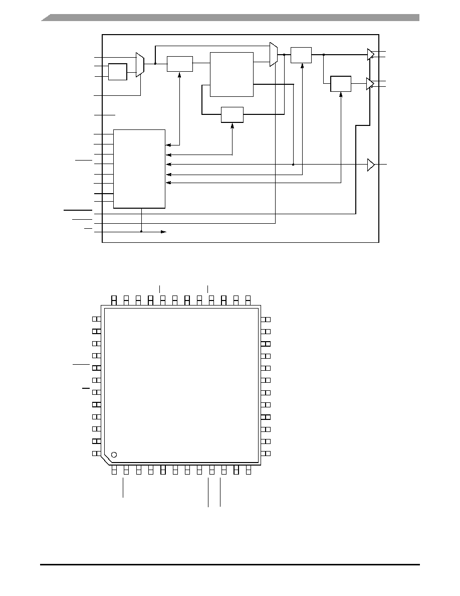
Figure 1. MPC92433≠Generic Logic Diagram
Figure 2. 48-Lead Package Pinout (Top View)
˜P
XTAL
PLL
˜NB
˜NA
˜M
f
REF
f
VCO
f
QA
f
QB
REF_CLK
XTAL1
XTAL2
REF_SEL
TEST_EN
SDA
SCL
ADR[1:0]
PLOAD
M[9:0]
NA[2:0]
NB
P
CLK_STOPx
BYPASS
MR
QA
QB
LOCK
PLL
Configuration
Registers
I
2
C Control
It is recommended to use an external
RC filter for the analog V
CC_PLL
supply
pin. Please see the application section
for details.
36
35
34
33
32
31
30
29
28
27
26
25
24
23
22
21
20
19
18
17
16
15
14
13
1
2
3
4
5
6
7
8
9
10
11
12
37
38
39
40
41
42
43
44
45
46
47
48
MPC92433
M9
M8
M7
M6
M5
GND
M4
M3
M2
M1
M0
V
CC
GND
NA2
NA1
NA0
PLOAD
V
CC
MR
SDA
SCL
ADR1
ADR0
P
V
CC
NB
V
CC
QA
QA
GN
D
V
CC
QB
QB
GN
D
LO
CK
TE
ST
_EN
V
CC
BY
PA
SS
GN
D
V
CC
V
CC
_P
L
L
RE
F_
SE
L
RE
F_
CL
K
GN
D
C
L
K_
ST
OP
A
CL
K_
ST
OPB
XT
AL
1
XT
AL
2
Advanced Clock Drivers Devices
Freescale Semiconductor
3
MPC92433
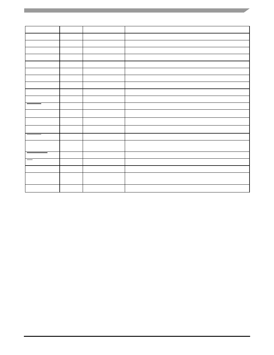
Table 1. Signal Configuration
Pin
I/O
Type
Function
XTAL1, XTAL2
Input
Analog
Crystal oscillator interface
REF_CLK
Input
LVCMOS
PLL external reference input
REF_SEL
Input
LVCMOS
Selects the reference clock input
QA
Output
Differential LVPECL
High frequency clock output
QB
Output
Differential LVPECL
High frequency clock output
LOCK
Output
LVCMOS
PLL lock indicator
M[9:0]
Input
LVCMOS
PLL feedback divider configuration
NA[2:0]
Input
LVCMOS
PLL post-divider configuration for output QA
NB
Input
LVCMOS
PLL post-divider configuration for output QB
P
Input
LVCMOS
PLL pre-divider configuration
P_LOAD
Input
LVCMOS
Selects the programming interface
SDA
I/O
LVCMOS
I
2
C data
SCL
Input
LVCMOS
I
2
C clock
ADR[1:0]
Input
LVCMOS
Selectable two bits of the I
2
C slave address
BYPASS
Input
LVCMOS
Selects the static circuit bypass mode
TEST_EN
Input
LVCMOS
Factory test mode enable. This input must be set to logic low level in all
applications of the device.
CLK_STOPx
Input
LVCMOS
Output Qx disable in logic low state
MR
Input
LVCMOS
Device master reset
GND
Supply
Ground
Negative power supply
V
CC_PLL
Supply
V
CC
Positive power supply for the PLL (analog power supply). It is recommended
to use an external RC filter for the analog power supply pin V
CC_PLL
.
V
CC
Supply
V
CC
Positive power supply for I/O and core
Advanced Clock Drivers Devices
4
Freescale Semiconductor
MPC92433
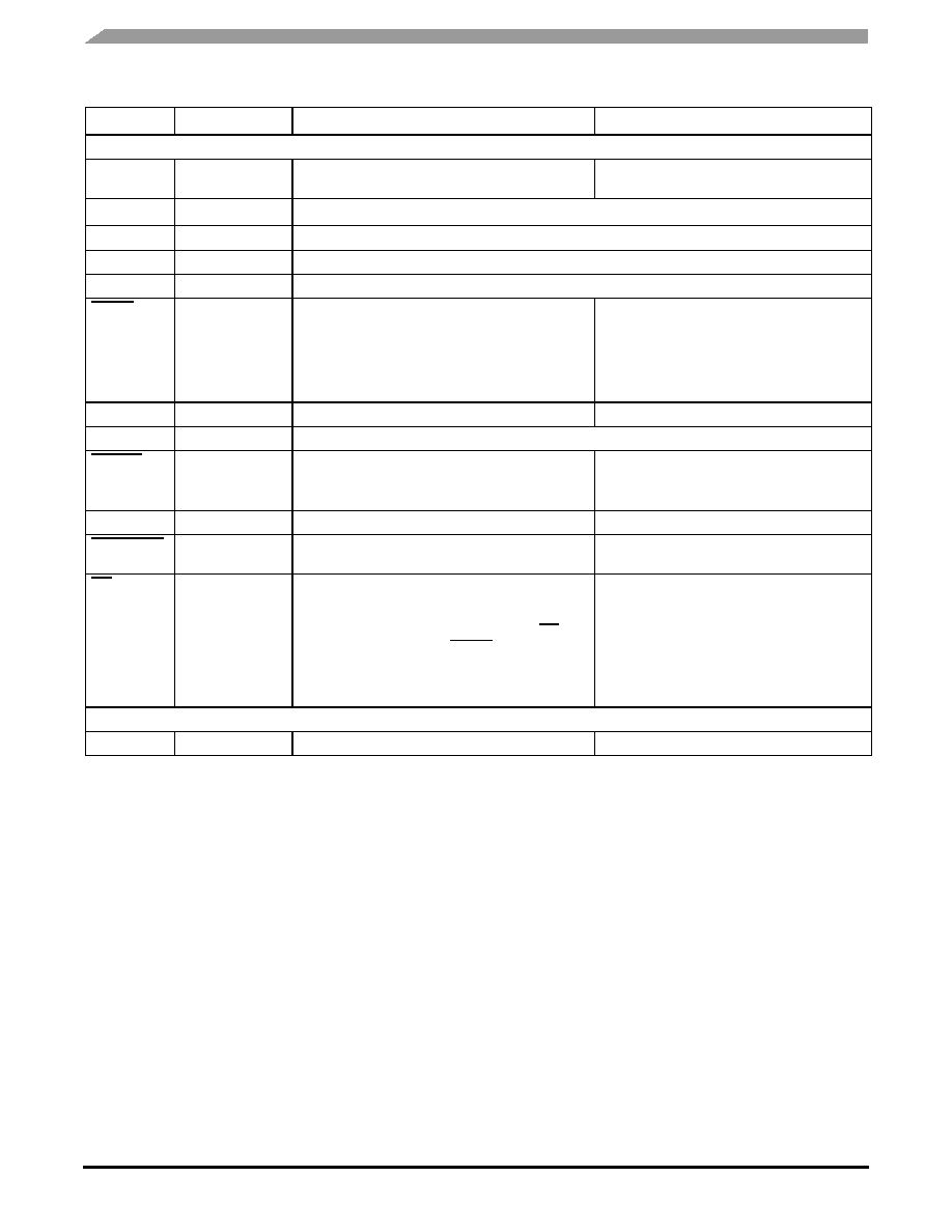
Table 2. Function Table
Control
Default
(1)
1. Default states are set by internal input pull-up or pull-down resistors of 75 k
.
0
1
Inputs
REF_SEL
1
Selects REF_CLK input as PLL reference clock
Selects the XTAL interface as PLL reference
clock
M[9:0]
01 1111 0100b
(2)
2. If f
REF
= 16 MHz, the default configuration will result in an output frequency of 250 MHz.
PLL feedback divider (10-bit) parallel programming interface
NA[2:0]
010
PLL post-divider parallel programming interface. See
Table 9
NB
0
PLL post-divider parallel programming interface. See
Table 9
P
1
PLL pre-divider parallel programming interface. See
Table 8
PLOAD
0
Selects the parallel programming interface. The
internal PLL divider settings (M, NA, NB and P) are
equal to the setting of the hardware pins. Leaving the
M, NA, NB and P pins open (floating) results in a
default PLL configuration with f
OUT
= 250 MHz. See
application/programming section.
Selects the serial (I
2
C) programming interface.
The internal PLL divider settings (M, NA, NB and
P) are set and read through the serial interface.
ADR[1:0]
00
Address bit = 0
Address bit = 1
SDA, SCL
See Programming the MPC92433
BYPASS
1
PLL function bypassed
f
QA
=f
REF
˜ N
A
and
f
QB
=f
REF
˜ (N
A
∑ N
B
)
PLL function enabled
f
QA
= (f
REF
˜ P) ∑ M ˜ N
A
and
f
QB
= (f
REF
˜ P) ∑ M ˜ (N
A
∑ N
B
)
TEST_EN
0
Application mode. Test mode disabled.
Factory test mode is enabled
CLK_STOPx
1
Output Qx is disabled in logic low state. Synchronous
disable is only guaranteed if NB = 0.
Output Qx is synchronously enabled
MR
The device is reset. The output frequency is zero and
the outputs are asynchronously forced to logic low
state.
After releasing reset (upon the rising edge of MR and
independent on the state of PLOAD), the MPC92433
reads the parallel interface (M, NA, NB and P) to
acquire a valid startup frequency configuration. See
application/programming section.
The PLL attempts to lock to the reference signal.
The t
LOCK
specification applies.
Outputs
LOCK
PLL is not locked
PLL is frequency locked
Advanced Clock Drivers Devices
Freescale Semiconductor
5
MPC92433
Table 3. General Specifications
Symbol
Characteristics
Min
Typ
Max
Unit
Condition
V
TT
Output Termination Voltage
V
CC
≠ 2
V
MM
ESD Protection (Machine Model)
200
V
HBM
ESD Protection (Human Body Model)
2000
V
LU
Latch-Up Immunity
200
mA
C
IN
Input Capacitance
4.0
pF
Inputs
JA
LQFP 48 Thermal Resistance Junction to Ambient
JESD 51-3, single layer test board
JESD 51-6, 2S2P multilayer test board
69
64
53
50
∞C/W
∞C/W
∞C/W
∞C/W
Natural convection
200 ft/min
Natural convection
200 ft/min
JC
LQFP 48 Thermal Resistance Junction to Case
TBD
TBD
∞C/W MIL-SPEC 883E
Method 1012.1
Table 4. Absolute Maximum Ratings
(1)
Symbol
Characteristics
Min
Max
Unit
Condition
V
CC
Supply Voltage
≠0.3
3.9
V
V
IN
DC Input Voltage
(2)
≠0.3
V
CC
+ 0.3
V
V
OUT
DC Output Voltage
≠0.3
V
CC
+ 0.3
V
I
IN
DC Input Current
±20
mA
I
OUT
DC Output Current
±50
mA
T
S
Storage Temperature
≠65
125
∞C
1. Absolute maximum continuous ratings are those maximum values beyond which damage to the device may occur. Exposure to these
conditions or conditions beyond those indicated may adversely affect device reliability. Functional operation at absolute-maximum-rated
conditions is not implied.
2. All input pins including SDA and SCL pins.
Advanced Clock Drivers Devices
6
Freescale Semiconductor
MPC92433
Table 5. DC Characteristics (V
CC
= 3.3 V ± 5%, T
J
= ≠40∞C to +85∞C)
Symbol
Characteristics
Min
Typ
Max
Unit
Condition
LVCMOS Control Inputs (M[9:0], N[2:0], ADDR[1:0], NB, P, CLK_STOPx, BYPASS, MR, REF_SEL, TEST_EN, PLOAD)
V
IH
Input High Voltage
2.0
--
V
CC
+ 0.3
V
LVCMOS
V
IL
Input Low Voltage
--
--
0.8
V
LVCMOS
I
IN
Input Current
(1)
--
--
±200
µA
V
IN
= V
CC
or GND
I
2
C Inputs (SCL, SDA)
V
IH
Input High Voltage
2.0
--
V
CC
+ 0.3
V
LVCMOS
V
IL
Input Low Voltage
--
--
0.8
V
LVCMOS
I
IN
Input Current
--
--
±10
µA
LVCMOS Output (LOCK)
V
OH
Output High Voltage
2.4
--
--
V
I
OH
= ≠4 mA
V
OL
Output Low Voltage
--
--
0.4
V
I
OL
= 4 mA
I
2
C Open-Drain Output (SDA)
V
OL
Input Low Voltage
--
--
0.4
V
I
OL
= 4 mA
Differential Clock Output QA, QB
(2)
V
OH
Output High Voltage
V
CC
≠ 1.05
--
V
CC
≠ 0.74
V
LVPECL
V
OL
Output Low Voltage
V
CC
≠ 1.95
--
V
CC
≠ 1.60
V
LVPECL
V
O(P-P)
Output Peak-to-Peak Voltage
0.5
0.6
1.0
V
Supply current
I
CC_PLL
Maximum PLL Supply Current
--
--
10
mA
V
CC_PLL
Pins
I
CC
Maximum Supply Current
--
--
150
mA
All V
CC
Pins
1. Inputs have pull-down resistors affecting the input current.
2. Outputs terminated 50
to V
TT
= V
CC
≠ 2 V.
Advanced Clock Drivers Devices
Freescale Semiconductor
7
MPC92433
Table 6. AC Characteristics (V
CC
= 3.3 V ± 5%, T
J
= ≠40∞C to +85∞C
(1)
(2)
1. AC specifications are subject to change.
2. AC characteristics apply for parallel output termination of 50
to V
TT
.
Symbol
Characteristics
Min
Typ
Max
Unit
Condition
f
XTAL
Crystal Interface Frequency Range
15
16
20
MHz
f
REF
FREF_EXT Reference Frequency Range
15
20
MHz
f
VCO
VCO Frequency Range
(3)
3. The input frequency f
XTAL
, the PLL divider M and P must match the VCO frequency range: f
VCO
= f
XTAL
∑ M ˜ P. The feedback divider M is
limited to 170 <= M <= 357 (for P=2) and 340 <= M <= 714 (for P=4) for stable PLL operation.
1360
2856
MHz
f
MAX
Output Frequency
(4)
N= ˜2
N= ˜4
N= ˜6
N= ˜8
N= ˜12
N= ˜16
N= ˜32
4. Output frequency for Q
A
, Q
B
if N
B
=0. With N
B
=1 the Q
B
output frequency is half of the Q
A
output frequency.
680
340
226.67
170
113.30
178.50
42.50
1428
714
476
357
238
178.50
89.25
MHz
MHz
MHz
MHz
MHz
MHz
MHz
f
SCL
Serial Interface (I
2
C) Clock Frequency
0
0.4
MHz
t
P,MIN
Minimum Pulse Width
(P_LOAD)
50
ns
DC
Output Duty Cycle
45
50
55
%
t
SK(O)
Output-to-Output Skew
NB=0 (f
QA
= f
QB
)
NB=1 (f
QA
= 2∑ f
QB
)
38
96
ps
ps
t
r
, t
f
Output Rise/Fall Time (QA, QB)
0.05
0.3
ns
20% to 80%
t
r
, t
f
Output Rise/Fall Time (SDA)
250
ns
C
L
= 400 pF
t
P_EN
Output Enable Time (CLKSTOPx to QA, QB)
0
2 ∑ T
Qx
T
Qx
= Output period
t
P_DIS
Output Disable Time (CLKSTOPx to QA, QB)
0
1.5 ∑ T
Qx
T
Qx
= Output period
t
JIT(CC)
Cycle-to-Cycle Jitter (RMS)
(5)
N= ˜2, ˜4, ˜6, ˜8
N= ˜12
N= ˜16, ˜32
5. Maximum cycle jitter measured at the lowest VCO frequency. Refer to Figure 8 for the cycle jitter vs. frequency characterisitics.
15
20
30
ps
ps
ps
t
JIT(PER)
Period Jitter (RMS)
(6)
N= ˜2
N= ˜4
N= ˜6
N= ˜8
N= ˜12
N= ˜16
N= ˜32
6. Maximum period jitter measured at the lowest VCO frequency. Refer to Figure 9 for the period jitter vs. frequency characterisitics.
8
10
12
13
17
23
29
ps
ps
ps
ps
ps
ps
ps
N
REF(UNLOCK)
Number of missing reference clock cycles to
declare an out of LOCK condition
(7)
7. See the
LOCK Detect
section on page 13.
2
t
LOCK
Maximum PLL Lock Time
10
ms

Advanced Clock Drivers Devices
8
Freescale Semiconductor
MPC92433
Output Frequency Configuration
The MPC92433 is a programmable frequency source
(synthesizer) and supports an output frequency range of
42.5 ≠ 1428 MHz. The output frequency f
OUT
is a function of
the reference frequency f
REF
and the three internal PLL
dividers P, M, and N. f
OUT
can be represented by this formula:
f
OUT
= (f
REF
˜ P) ∑ M ˜ (N
A
,
B
) (1)
The M, N and P dividers require a configuration by the user
to achieve the desired output frequency. The output divider,
N
A,
determines the achievable output frequency range (see
Table 7
). The PLL feedback-divider M is the frequency
multiplication factor and the main variable for frequency
synthesis. For a given reference frequency f
REF
, the PLL
feedback-divider M must be configured to match the
specified VCO frequency range in order to achieve a valid
PLL configuration:
f
VCO
= (f
REF
˜ P) ∑ M and (2)
1360
f
VCO
2856 (3)
The output frequency may be changed at any time by
changing the value of the PLL feedback divider M. The
smallest possible output frequency change is the synthesizer
granularity G (difference in f
OUT
when incrementing or
decrementing M). At a given reference frequency, G is a
function of the PLL pre-divider P and post-divider N:
G = f
REF
˜ (P ∑ N
A,B
) (4)
The N
B
divider configuration determines if the output Q
B
generates a 1:1 or 2:1 frequency copy of the Q
A
output signal.
The purpose of the PLL pre-divider P is to situated the PLL
into the specified VCO frequency range f
VCO
(in combination
with M). For a given output frequency, P = 4 results in a
smaller output frequency granularity G, P = 2 results a larger
output frequency granularity G and also increases the PLL
bandwidth compared to the P = 2 setting.
The following example illustrates the output frequency
range of the MPC92433 using a 16-MHz reference
frequency.
Example Output Frequency Configuration
If a reference frequency of 16 MHz is available, an output
frequency at Q
A
of 250 MHz and a small frequency
granularity is desired, the following steps would be taken to
identify the appropriate P, M, and N configuration:
1.
Use
Table 7
to select the output divider, N
A
, that
matches the desired output frequency or frequency
range. According to
Table 7
, a target output frequency
of 250 MHz falls in the f
OUT
range of 170 to 357 MHz
and requires to set N
A
= 8
2.
Calculate the VCO frequency f
VCO
= f
OUT
∑ N
A
, which is
2000 MHz in this example.
3.
Determine the PLL feedback divider: M = f
VCO
˜ P.
The smallest possible output granularity in this example
calculation is 500 kHz (set P = 4). M calculates to a
value of 2000 ˜ 4 = 500.
4.
Configure the MPC92433 with the obtained settings:
M[9:0] = 0111110100b (binary number for M=500)
N
A
[2:0] = 010
(˜8 divider, see
Table 9
)
P = 1
(˜4 divider, see
Table 8
)
N
B
= 0
(f
OUT, QB
= f
OUT, QA
)
5.
Use either parallel or serial interface to apply the
setting. The I
2
C configuration bytes for this example
are:
PLL_H=01010010b and PLL_L=11110100b.
See
Table 13
and
Table 14
for register maps.
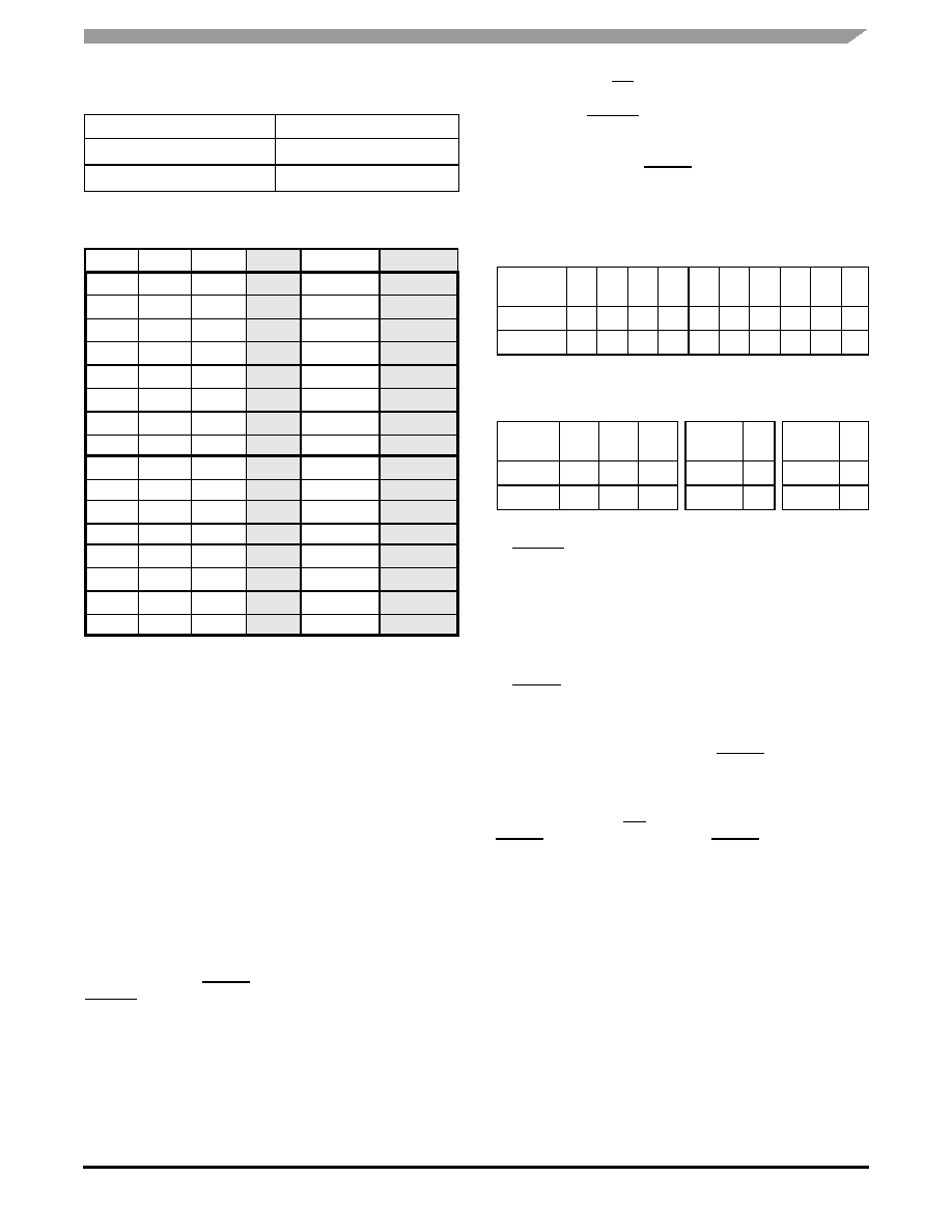
Table 7. Frequency Ranges (f
REF
=16 MHz)
f
OUT
(Q
A
) [MHz]
N
A
M
P
G [MHz]
680≠1428
N
A
=2
170-357
2
4
340-714
4
2
340≠714
N
A
=4
170-357
2
2
340-714
4
1
226.67≠476
N
A
=6
170-357
2
1.33
340-714
4
0.66
170≠357
N
A
=8
170-357
2
1
340-714
4
0.5
113.33≠238
N
A
=12
170-357
2
0.66
340-714
4
0.33
85≠178.5
N
A
=16
170-357
2
0.5
340-714
4
0.25
42.5≠89.25
N
A
=32
170-357
2
0.25
340-714
4
0.125
Advanced Clock Drivers Devices
Freescale Semiconductor
9
MPC92433
PLL Divider Configuration
Programming the MPC92433
The MPC92433 has a parallel and a serial configuration
interface. The purpose of the parallel interface is to directly
configure the PLL dividers through hardware pins without the
overhead of a serial protocol. At device startup, the device
always obtains an initial PLL frequency configuration through
the parallel interface. The parallel interface does not support
reading the PLL configuration.
The serial interface is I
2
C compatible. It allows reading and
writing devices settings by accessing internal device
registers. The serial interface is designed for host-controller
access to the synthesizer frequency settings for instance in
frequency-margining applications.
Using the Parallel Interface
The parallel interface supports write-access to the PLL
frequency setting directly through 15 configuration pins (P,
M[9:0], NA[2:0], and NB). The parallel interface must be
enabled by setting PLOAD to logic low level. During
PLOAD = 0, any change of the logical state of the P, M[9:0],
NA[2:0], and NB pins will immediately affect the internal PLL
divider settings, resulting in a change of the internal VCO-
frequency and the output frequency. The parallel interface
mode disables the I
2
C write-access to the internal registers;
however, I
2
C read-access to the internal configuration
registers is enabled.
Upon startup, when the device reset signal is released
(rising edge of the MR signal), the device reads its startup
configuration through the parallel interface and independent
on the state of PLOAD. It is recommended to provide a valid
PLL configuration for startup. If the parallel interface pins are
left open, a default PLL configuration will be loaded. After the
low-to-high transition of PLOAD, the configuration pins have
no more effect and the configuration registers are made
accessible through the serial interface.
Using the I
2
C Interface
PLOAD = 1 enables the programming and monitoring of
the internal registers through the I
2
C interface. Device
register access (write and read) is possible through the 2-wire
interface using SDA (configuration data) and SCL
(configuration clock) signals. The MPC92433 acts as a slave
device at the I
2
C bus. For further information on I
2
C it is
recommended to refer to the I
2
C bus specification (version
2.1).
PLOAD = 0 disables the I
2
C-write-access to the configura-
tion registers and any data written into the register is ignored.
However, the MPC92433 is still visible at the I
2
C interface
and I
2
C transfers are acknowledged by the device. Read-ac-
cess to the internal registers during PLOAD = 0 (parallel pro-
gramming mode) is supported.
Note that the device automatically obtains a configuration
using the parallel interface upon the release of the device
reset (rising edge of MR) and independent on the state of
PLOAD. Changing the state of the PLOAD input is not
supported when the device performs any transactions on the
I
2
C interface.
Programming Model and Register Set
The synthesizer contains two fully accessible configuration
registers (PLL_L and PLL_H) and a write-only command
register (CMD). Programming the synthesizer frequency
through the I
2
C interface requires two steps: 1) writing a valid
PLL configuration to the configuration registers and 2)
loading the registers into the PLL by an I
2
C command. The
PLL frequency is affected as a result of the second step.
This two-step procedure can be performed by a single I
2
C
transaction or by multiple, independent I
2
C transactions. An
alternative way to achieve small PLL frequency changes is to
use the increment or decrement commands of the
Table 8. Pre-PLL Divider P
P
Value
0
f
REF
˜ 2
1
f
REF
˜ 4
Table 9. Post-PLL Divider N
A
and N
B
N
A2
N
A1
N
A0
N
B
f
OUT
(Q
A
)
f
OUT
(Q
B
)
0
0
0
0
f
VCO
˜ 2
f
VCO
˜ 2
0
0
1
0
f
VCO
˜ 32
f
VCO
˜ 32
0
1
0
0
f
VCO
˜ 8
f
VCO
˜ 8
0
1
1
0
f
VCO
˜ 12
f
VCO
˜ 12
1
0
0
0
f
VCO
˜ 4
f
VCO
˜ 4
1
0
1
0
f
VCO
˜ 6
f
VCO
˜ 6
1
1
0
0
f
VCO
˜ 16
f
VCO
˜ 16
1
1
1
0
n/a
n/a
0
0
0
1
f
VCO
˜ 2
f
VCO
˜ 4
0
0
1
1
n/a
n/a
0
1
0
1
f
VCO
˜ 8
f
VCO
˜ 16
0
1
1
1
n/a
n/a
1
0
0
1
f
VCO
˜ 4
f
VCO
˜ 8
1
0
1
1
f
VCO
˜ 6
f
VCO
˜ 12
1
1
0
1
f
VCO
˜ 16
f
VCO
˜ 32
1
1
1
1
n/a
n/a
Table 10. Feedback Divider Configuration
Feedback
Divider M
9
8
7
6
5
4
3
2
1
0
Pin
M9 M8 M7 M6 M5 M4 M3 M2 M1 M0
Default
0
1
1
1
1
1
0
1
0
0
Table 11. PLL Pre/Post Divider Configuration (N, P)
Post-D.
NA
2
1
0
Post-D.
NB
NB
Pre-D.
P
P
Pin
NA2
NA1
NA0
Pin
NB
Pin
P
Default
0
1
0
Default
0
Default
1
Advanced Clock Drivers Devices
10
Freescale Semiconductor
MPC92433
synthesizer, which have an immediate effect on the PLL
frequency.
Figure 3. I
2
C Mode Register Set
Figure 3
illustrates the synthesizer register set. PLL_L and
PLL_H store a PLL configuration and are fully accessible
(Read/Write) by the I
2
C bus. CMD (Write only) accepts
commands (LOAD, GET, INC, DEC) to update registers and
for direct PLL frequency changes.
Set the synthesizer frequency:
1) Write the PLL_L and PLL_H registers with a new
configuration (see
Table 13
and
Table 14
for register
maps)
2) Write the LOAD command to update the PLL dividers
by the current PLL_L, PLL_H content.
Read the synthesizer frequency:
1) Write the GET commands to update the PLL_L,
PLL_H registers by the PLL divider setting
2) Read the PLL_L, PLL_H registers through I
2
C
Change the synthesizer frequency in small steps:
1) Write the INC or DEC command to change the PLL
frequency immediately. Repeat at any time if desired.
LOAD and GET are inverse command to each other.
LOAD updates the PLL dividers and GET updates the
configuration registers. A fast and convenient way to change
the PLL frequency is to use the INC (increment M) and DEC
(decrement M) commands of the synthesizer. INC (DEC)
directly increments (decrements) the PLL-feedback divider M
and immediately changes the PLL frequency by the smallest
step G (see
Table 7
for the frequency granularity G). The INC
and DEC commands are designed for multiple and rapid PLL
frequency changes as required in frequency margining
applications. INC and DEC do not require the user to update
the PLL dividers by the LOAD command, INC and DEC do
not update the PLL_L and PLL_H registers either (use LOAD
for an initial PLL divider setting and, if desired, use GET to
read the PLL configuration). Note that the synthesizer does
not check any boundary conditions such as the VCO
frequency range. Applying the INC and DEC commands
could result in invalid VCO frequencies (VCO frequency
beyond lock range).
Register Maps
Register 0x00 (PLL_L) contains the least significant bits of
the PLL feedback divider M.
Register content:
M[7:0]
PLL feedback-divider M, bits 7≠0
Register 0x01 (PLL_H) contains the two most significant
bits of the PLL feedback divider M, four bits to control the PLL
post-dividers N and the PLL pre-divider P. The bit 0 in PLL_H
register indicates the lock condition of the PLL and is set by
the synthesizer automatically. The LOCK state is a copy of
the PLL lock signal output (LOCK). A write-access to LOCK
has no effect.
Register content:
M[9:8]
PLL feedback-divider M, bits 9≠8
NA[2:0]
PLL post-divider N
A
, see
Table 9
NB
PLL post-divider N
B
, see
Table 9
P
PLL pre-divider P, see
Table 8
LOCK
Copy of LOCK output signal (read-only)
Note that the LOAD command is required to update the
PLL dividers by the content of both PLL_L and PLL_H
registers.
Register 0xF0 (CMD) is a write-only command register.
The purpose of CMD is to provide a fast way to increase or
decrease the PLL frequency and to update the registers. The
register accepts four commands, INC (increment M), DEC
(decrement M), LOAD and GET (update registers). It is
recommended to write the INC, DEC commands only after a
valid PLL configuration is achieved. INC and DEC only affect
the M-divider of the PLL (PLL feedback). Applying INC and
DEC commands can result in a PLL configuration beyond the
specified lock range and the PLL may lose lock. The
MPC92433 does not verify the validity of any commands
such as LOAD, INC, and DEC. The INC and DEC commands
change the PLL feedback divider without updating PLL_L
and PLL_H.
Configuration Latches
I
2
C Registers
I
2
C Access
Synthesizer ≠ PLL
P
N
M
LOAD/GET
PLL_L (R/W)
0x00
PLL_H (R/W)
0x01
CMD (W)
0xF0
Table 12. Configuration Registers
Address
Name
Content
Access
0x00
PLL_L
Least significant 8 bits of M
R/W
0x01
PLL_H Most significant 2 bits of M, P, N
A
,
N
B
, and lock state
R/W
0xF0
CMD
Command register (write only)
W only
Table 13. PLL_L (0x00, R/W) Register
Bit
7
6
5
4
3
2
1
0
Name
M7
M6
M5
M4
M3
M2
M1
M0
Table 14. PLL_H (0x01, R/W) Register
Bit
7
6
5
4
3
2
1
0
Name
M9
M8
NA2
NA1
NA0
NB
P
LOCK
Advanced Clock Drivers Devices
Freescale Semiconductor
11
MPC92433
I
2
C -- Register Access in Parallel Mode
The MPC92433 supports the configuration of the
synthesizer through the parallel interlace (PLOAD = 0) and
serial interface (PLOAD = 1). Register contents and the
divider configurations are not changed when the user
switches from parallel mode to serial mode. However, when
switching from serial mode to parallel mode, the PLL dividers
immediately reflect the logical state of the hardware pins
M[9:0], NA[2:0], NB, and P.
Applications using the parallel interface to obtain a PLL
configuration can use the serial interface to verify the divider
settings. In parallel mode (PLOAD = 0), the MPC92433
allows read-access to PLL_L and PLL_H through I
2
C (if
PLOAD = 0, the current PLL configuration is stored in PLL_L,
PLL_H. The GET command is not necessary and also not
supported in parallel mode). After changing from parallel to
serial mode (PLOAD = 1), the last PLL configuration is still
stored in PLL_L, PLL_H. The user now has full write and read
access to both configuration registers through the I
2
C bus
and can change the configuration at any time.
Programming the I
2
C Interface
The 7-bit I
2
C slave address of the MPC92433 synthesizer
is a combination of a 5-bit fixed addresses and two variable
bits which are set by the hardware pins ADR[1:0]. Bit 0 of the
MPC92433 slave address is used by the bus controller to
select either the read or write mode. '0' indicates a
transmission (I
2
C-WRITE) to the MPC92433. '1' indicates a
request for data (I
2
C-READ) from the synthesizer. The
hardware pins ADR1 and ADR0 and should be individually
set by the user to avoid address conflicts of multiple
MPC92433 devices on the same I
2
C bus.
Write Mode (R/W = 0)
The configuration registers are written by the bus
controller by the initiation of a write transfer with the
MPC92433 slave address (first byte), followed by the address
of the configuration register (second byte: 0x00, 0x01 or
0xF0), and the configuration data byte (third byte). This
transfer may be followed by writing more registers by sending
the configuration register address followed by one data byte.
Each byte sent by the bus controller is acknowledged by the
MPC92433. The transfer ends by a stop bit sent by the bus
controller. The number of configuration data bytes and the
write sequence are not restricted.
Table 15. CMD (0xF0): PLL Command (Write-Only)
Command
Op-Code
Description
INC
xxxx0001b
(0x01)
Increase internal PLL frequency
M:=M+1
DEC
xxxx0010b
(0x02)
Decrease internal PLL frequency
M:=M-1
LOAD
xxxx0100b
(0x04)
Update the PLL divider config.
PLL divider M, N, P:=PLL_L, PLL_H
GET
xxxx1000b
(0x08)
Update the configuration registers
PLL_L, PLL_H:=PLL divider M, N, P
Table 16. PLL Configuration in Parallel and Serial Modes
PLL
Configuration
Parallel
Serial (Registers
PLL_L, PLL_H)
M[9:0]
Set pins M9≠M0
M[9:0] (R/W)
NA[2:0]
Set pins NA2...NA0
NA[2:0] (R/W)
NB
Set pin NB
NB (R/W)
P
Set pin P
P (R/W)
LOCK status
LOCK pin 26
LOCK (Read only)
Table 17. I
2
C Slave Address
Bit
7
6
5
4
3
2
1
0
Value
1
0
1
1
0
Pin
ADR1
Pin
ADR0
R/W
Table 18. Complete Configuration Register Write Transfer
1 bit
7 bits
1 bit
1 bit
8 bits
1 bit
8 bits
1 bit
8 bits
1 bit
8 bits
1 bit
1 bit
Start
Slave address
R/W
ACK
&PLL_H
ACK
Config-Byte 1
ACK
&PLL_L
ACK
Config-Byte 2
ACK
Stop
10110xx
(1)
1. xx = state of ADR1, ADR0 pins
0
0x01
Data
0x00
Data
Master
Master
Mast
Slave
Master
Slave
Master
Slave
Master
Slave
Master
Slave
Mast
Advanced Clock Drivers Devices
12
Freescale Semiconductor
MPC92433
Read Mode (R/W = 1)
The configuration registers are read by the bus controller
by the initiation of a read transfer. The MPC92433 supports
read transfers immediately after the first byte without a
change in the transfer direction. Immediately after the bus
controller sends the slave address, the MPC92433
acknowledges and then sends both configuration register
PLL_L and PLL_H (back-to-back) to the bus controller. The
CMD register cannot be read. In order to read the two
synthesizer registers and the current PLL configuration
setting, the user can 1) read PLL_L, PLL_H, write the GET
command (loads the current configuration into PLL_L,
PLL_H) and read PLL_L, PLL_H again. Note that the PLL_L,
PLL_H registers and divider settings may not be equivalent
after the following cases:
a.
Writing the INC command
b.
Writing the DEC command
c.
Writing PLL_L, PLL_H registers with a new
configuration and not writing the LOAD command.
Device Startup
General Device Configuration
It is recommended to reset the MPC92433 during or
immediately after the system powers up (MR = 0). The device
acquires an initial PLL divider configuration through the
parallel interface pins M[9:0], NA[2:0], N, and P
(1)
with the
low-to-high transition of MR
(2)
. PLL frequency lock is
achieved within the specified lock time (t
LOCK
) and is
indicated by an assertion of the LOCK signal which
completes the startup procedure. It is recommended to
disable the outputs (CLK_STOPx = 0) until PLL lock is
achieved to suppress output frequency transitions. The
output frequency can be reconfigured at any time through
either the parallel or the serial interface.
Note that a PLL configuration obtained by the parallel
interface can be read through I
2
C independent on the current
programming mode (parallel or serial). Refer to the I2C --
Register Access in Parallel Mode section for additional
information on how to read a PLL startup configuration
through the I
2
C interface.
Starting-Up Using the Parallel Interface
The simplest way to use the MPC92433 is through the
parallel interface. The serial interface pins (SDA, SDL) and
ADDR[1:0]) can be left open and PLOAD is set to logic low.
After the release of MR and at any other time the PLL/output
frequency configuration is directly set to through the M[9:0],
NA[2:0], NB, and P pins.
Start-Up Using the Serial (I
2
C) Interface
Figure 4. Start-Up Using I
2
C Interface
Set PLOAD = 1, CLK_STOPx = L and leave the parallel
interface pins (M[9:0], NA[2:0], N, and P) open. The PLL
dividers are configured by the default configuration at the low-
to-high transition of MR. This initial PLL configuration can be
re-programmed to the final VCO frequency at any time
through the serial interface. After the PLL achieved lock at the
desired VCO frequency, enable the outputs by setting
CLK_STOPx = H. PLL lock and re-lock (after any
configuration change through M or P) is indicated by LOCK
being asserted.
Table 19. Configuration Register Read Transfer
1 bit
7 bits
1 bit
1 bit
8 bits
1 bit
8 bits
1 bit
1 bit
Start
Slave address
R/W
ACK
PLL_L
ACK
PLL_H
ACK
Stop
10110xx
(1)
1. xx = state of ADR1, ADR0 pins
1
Data
Data
Master
Master
Mast
Slave
Slave
Mast
Slave
Master
Slave
1. The parallel interface pins M[9:0], NA[2:0], N, and P may be left open (floating). In this case the initial PLL configuration will have the default
setting of M = 500, P = 1, NA[2:0] = 010, NB = 0, resulting in an internal VCO frequency of 2000 MHz (f
ref
= 16 MHz) and an output frequency
of 250 MHz.
2. The initial PLL configuration is independent on the selected programming mode (PLOAD low or high)
V
CC
MR
P, M, N
PLOAD
LOCK
CLK_STOPx
QA, QB
Stable & Valid
Selects I
2
C
Acquiring Lock
PLL Lock
Disabled (Low)
t
PLH
Active
Advanced Clock Drivers Devices
Freescale Semiconductor
13
MPC92433
LOCK Detect
The LOCK detect circuitry indicates the frequency-lock
status of the PLL by setting and resetting the pin LOCK and
register bit LOCK simultaneously. After acquiring an internal
frequency lock state, the assertion of the LOCK signal is
delayed at least 256 reference clock cycles to prevent
signaling temporary PLL locks during frequency transitions.
The LOCK signal is deasserted when the PLL lost lock, for
instance when the reference clock is removed: the LOCK
signal goes low after missing at least two f
ref
clock cycles
(N
REF(UNLOCK)
). The PLL may also lose lock when the PLL
feedback-divider M or pre-divider P is changed or the
DEC/INC command is issued. The PLL may not lose lock as
a result of slow reference frequency changes. In any case of
losing LOCK, the PLL attempts to re-lock to the reference
frequency.
Output Clock Stop
Asserting CLK_STOPx will stop the respective output
clock in logic low state. The CLK_STOPx control is internally
synchronized to the output clock signal, therefore, enabling
and disabling outputs does not produce runt pulses. See
Figure 5
.The clock stop controls of the QA and QB outputs
are independent on each other. If the QB runs at half of the
QA output frequency and both outputs are enabled at the
same time, the first clock pulse of QA may not appear at the
same time of the first QB output. (See
Figure 6
.) Concident
rising edges of QA and QB stay synchronous after the
assertion and de-assertion of the CLK_STOPx controls.
Asserting MR always resets the output divider to a logic low
output state, with the risk of producing an output runt pulse.
Figure 5. Clock Stop Timing for NB = 0 (f
QA
= f
QB
)
Figure 6. Clock Stop Timing for NB = 1 (f
QA
= 2 f
QB
)
CLK_STOPx
Qx
(Disable)
(Enable)
(Enable)
t
P_DIS
t
P_EN
CLK_STOPA,B
QA
QB
(Disable)
(Enable)
(Enable)
Advanced Clock Drivers Devices
14
Freescale Semiconductor
MPC92433
Frequency Operating Range
Table 20. MPC92433 Frequency Operating Range for P=2
f
VCO
[MHz] (parameter: f
REF
in MHz)
Output frequency for f
XTAL
=16 MHz (parameter N)
M
M[9:0]
15
16
18
20
2
4
6
8
12
16
32
170
0010101010
1360
1530
1700
680
340
226.67
170
113.33
85
42.50
180
0010110100
1440
1620
1800
720
360
240.00
180
120.00
90
45.00
190
0010111110
1425
1520
1710
1900
760
380
253.33
190
126.67
95
47.50
200
0011001000
1500
1600
1800
2000
800
400
266.67
200
133.33
100
50.00
210
0011010010
1575
1680
1890
2100
840
420
280.00
210
140.00
105
52.50
220
0011011100
1650
1760
1980
2200
880
440
293.33
220
146.67
110
55.00
230
0011100110
1725
1840
2070
2300
920
460
306.67
230
153.33
115
57.50
240
0011110000
1800
1920
2160
2400
960
480
320.00
240
160.00
120
60.00
250
0011111010
1875
2000
2250
2500
1000
500
333.33
250
166.67
125
62.50
260
0100000100
1950
2080
2340
2600
1040
520
346.67
260
173.33
130
65.00
270
0100001110
2025
2160
2430
2700
1080
540
360.00
270
180.00
135
67.50
280
0100011000
2100
2240
2520
2800
1120
560
373.33
280
186.67
140
70.00
290
0100100010
2175
2320
2610
1160
580
386.67
290
193.33
145
72.50
300
0100101100
2250
2400
2700
1200
600
400.00
300
200.00
150
75.00
310
0100110110
2325
2480
2790
1240
620
413.33
310
206.67
155
77.50
320
0101000000
2400
2560
1280
640
426.67
320
213.33
160
80.00
330
0101001010
2475
2640
1320
660
440.00
330
220.00
165
82.50
340
0101010100
2550
2720
1360
680
453.33
340
226.67
170
85.00
350
0101011110
2625
2800
1400
700
466.67
350
233.33
175
87.50
357
0101100101
2667.5
2856
1428
714
476.00
357
238.00
178.50
89.25
Advanced Clock Drivers Devices
Freescale Semiconductor
15
MPC92433
Table 21. MPC92433 Frequency Operating Range for P=4
f
VCO
[MHz] (parameter: f
REF
in MHz)
Output frequency for f
XTAL
=16 MHz (parameter N)
M
M[9:0]
15
16
18
20
2
4
6
8
12
16
32
340
0101010100
1360
1530
1700
680
340
226.67
170
113.33
85.0
42.50
350
0101011110
1400
1575
1750
700
350
233.33
175
116.67
87.5
43.75
360
0101101000
1440
1620
1800
720
360
240.00
180
120.00
90.0
45.00
370
0101110010
1387.5
1480
1665
1850
740
370
246.67
185
123.33
92.5
46.25
380
0101111100
1425.0
1520
1710
1900
760
380
253.33
190
126.67
95.0
47.50
390
0110000110
1462.5
1560
1755
1950
780
390
260.00
195
130.00
97.5
48.75
400
0110010000
1500.0
1600
1800
2000
800
400
266.67
200
133.33
100.0
50.00
410
0110110010
1537.5
1640
1845
2050
820
410
273.33
205
136.67
102.5
51.25
420
0110100100
1575.0
1680
1890
2100
840
420
280.00
210
140.00
105.0
52.50
430
0110101110
1612.5
1720
1935
2150
860
430
286.67
215
143.33
107.5
53.75
440
0110111000
1650.0
1760
1980
2200
880
440
293.33
220
146.67
110.0
55.00
450
0111000010
1687.5
1800
2025
2250
900
450
300.00
225
150.00
112.5
56.25
460
0111001100
1725.0
1840
2070
2300
920
460
306.67
230
153.33
115.0
57.50
470
0111010110
1762.5
1880
2115
2350
940
470
313.33
235
156.67
117.5
58.75
480
0111100000
1800.0
1920
2160
2400
960
480
320.00
240
160.00
120.0
60.00
490
0111101010
1837.5
1960
2205
2450
980
490
326.67
245
163.33
122.5
61.25
500
0111110100
1875.0
2000
2250
2500
1000
500
333.33
250
166.67
125.0
62.50
510
0111111110
1912.5
2040
2295
2550
1020
510
340.00
255
170.00
127.5
63.75
520
1000001000
1950.0
2080
2340
2600
1040
520
346.67
260
173.33
130.0
65.00
530
1000010010
1987.5
2120
2475
2650
1060
530
353.33
265
176.67
132.5
66.25
540
1000011100
2025.0
2160
2520
2700
1080
540
360.00
270
180.00
135.0
67.50
550
1000100110
2062.5
2200
2565
2750
1100
550
366.67
275
183.33
137.5
68.75
560
1000110000
2100
2240
2610
2800
1120
560
373.33
280
186.67
140.0
70.00
570
1000111010
2137.5
2280
2565
2850
1140
570
380.00
285
190.00
142.5
71.25
580
1001000100
2175.0
2320
2610
1160
580
386.67
290
193.33
145.0
72.50
590
1001001110
2212.5
2360
2655
1180
590
393.33
295
196.67
147.5
73.75
600
1001011000
2250.0
2400
2700
1200
600
400.00
300
200.00
150.0
75.00
610
1001100010
2287.5
2440
2745
1220
610
406.67
305
203.33
152.5
76.25
620
1001101100
2325.0
2480
2790
1240
620
413.33
310
206.67
155.0
77.50
630
1001110110
2362.5
2520
2835
1260
630
420.00
315
210.00
157.5
78.75^
640
1010000000
2400.0
2560
1280
640
426.67
320
213.33
160.0
80.00
650
1010001010
2437.5
2600
1300
650
433.33
325
216.67
162.5
81.25
660
1010010100
2475.0
2640
1320
660
440.00
330
220.00
165
82.5
670
1010011110
2512.5
2680
1340
670
446.67
335
223.33
167.5
83.75
680
1010101000
2550.0
2720
1360
680
453.33
340
226.67
170.0
85.00
690
1010110010
2587.5
2760
1380
690
460.00
345
230.00
172.5
86.25
700
1010111100
2625.0
2800
1400
700
466.67
350
233.33
175.0
87.50
714
1011001010
2677.5
2856
1428
714
476.00
357
238.00
178.5
89.25
Advanced Clock Drivers Devices
16
Freescale Semiconductor
MPC92433
V
CC_PLL
Filter
The MPC92433 is a mixed analog/digital product. Its
analog circuitry is naturally susceptible to random noise,
especially if this noise is seen on the power supply pins.
Random noise on the V
CC_PLL
pin impacts the device AC
characteristics. The MPC92433 provides separate power
supplies for the digital circuitry (V
CC
) and the internal PLL
(V
CC_PLL
) of the device. The purpose of this design
technique is to isolate the high switching noise digital outputs
from the relatively sensitive internal analog phase-locked
loop. In digital system environments where it is more difficult
to minimize noise on the power supplies a second level of
isolation is recommended: a power supply filter on the
V
CC_PLL
pin for the MPC92433.
Figure 7. V
CC_PLL
Power Supply Filter
Figure 7
illustrates a recommended power supply filter
scheme.
The MPC92433 is most susceptible to noise with spectral
content in the 100 kHz to 1 MHz range. Therefore, the filter
should be designed to target this range. The key parameter
that needs to be met in the final filter design is the DC voltage
drop that will be seen between the V
CC
supply and the
V
CC_PLL
pin of the MPC92433. From the data sheet, the
V
CC_PLL
current (the current sourced through the V
CC_PLL
pin) is maximum 10 mA, assuming that a minimum of 2.985 V
must be maintained on the V
CC_PLL
pin. The resistor shown
in
Figure 7
must have a resistance of 10
≠
15
to meet the
voltage drop criteria. The minimum values for R
F
and the filter
capacitor C
F
are defined by the filter characteristics: the RC
filter should provide an attenuation greater than 40 dB for
noise whose spectral content is above 100 kHz. In the
recommended filter shown in
Figure 7
the filter cut-off
frequency is around 3.0
≠
4.5 kHz and the noise attenuation at
100 kHz is better than 42 dB.
As the noise frequency crosses the series resonant point
of an individual capacitor its overall impedance begins to look
inductive and thus increases with increasing frequency. The
parallel capacitor combination shown ensures that a low
impedance path to ground exists for frequencies well above
the bandwidth of the PLL.
The On-Chip Crystal Oscillator
The MPC92433 features an integrated on-chip crystal
oscillator to minimize system implementation cost. The
integrated oscillator is a Pierce-type that uses the crystal in
its parallel resonance mode. It is recommended to use a 15
to 20 MHz crystal with a load specification of C
L
= 10 pF.
Crystals with a load specification of C
L
= 20 pF may be used
at the expense of an resulting slightly higher frequency than
specified for the crystal. Externally connected capacitors on
both the XTAL_IN and XTAL_OUT pins are not required but
can be used to fine-tune the crystal frequency as desired.
The crystal, the trace and optional capacitors should be
placed on the board as close as possible to the MPC92433
XTAL_IN and XTAL_OUT pins to reduce crosstalk of active
signals into the oscillator. Short and wide traces further
reduce parasitic inductance and resistance. It is further
recommended to guard the crystal circuit by placing a ground
ring around the traces and oscillator components.
R
F
= 10≠15
V
CC
C
F
= 22
µF
10 nF
33...100 nF
V
CC_PLL
V
CC
MPC92433
7
Table 22. Recommended Crystal Specifications
Parameter
Value
Crystal Cut
Fundamental AT Cut
Resonance Mode
Parallel
Crystal Frequency
16≠20 MHz
Shunt Capacitance C
0
5≠7 pF
Load Capacitance C
L
10 pF
Advanced Clock Drivers Devices
Freescale Semiconductor
17
MPC92433
Jitter Performance of the MPC92433
Figure 8
and
Figure 9
illustrate the RMS jitter performance
of the MPC92433 across its specified VCO frequency range.
For some output dividers N, the cycle-to-cycle and period
jitter is a function of the VCO frequency and the output divider
N. The general trend is that as the output frequency
increases (higher VCO frequency and lower N-divider) the
MPC92433 output jitter decreases. Optimum jitter
performance can be achieved at higher VCO and output
frequencies.
For the output dividers of N=2, 4 and 6 the cycle-to-cycle
jitter does not depend on the VCO frequency. For the output
dividers of 2, 4 and 8 the period jitter does not depend on the
VCO frequency. The maximum cycle-to-cycle and period jitter
published in Table 6 (AC characteristics) correspond to the
jitter performance at the lowest VCO frequency limit. The
VCO frequency can be calculated using formula (2).
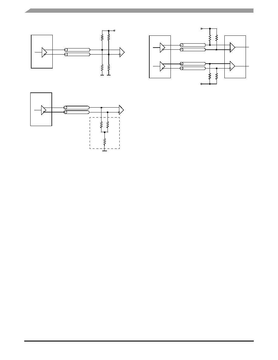
AC Test Reference and Output Termination
The MPC92433 LVPECL outputs are designed to drive
50 transmission lines and require a DC termination to
V
TT
= V
CC
≠ 2 V.
Figure 10
illustrates the AC test reference
for the MPC92433 as used in characterization and test of this
circuit. If a separate termination voltage (V
TT
) is not available,
applications may use alternative output termination methods
such as shown in
Figure 11
and
Figure 12
.
The high-speed differential output signals of the
MPC92433 are incompatible to single-ended LVCMOS
signals. In order to use the synthesizer in LVCMOS clock
signal environments, the dual-channel translator device
MC100ES60T23 provides the necessary level conversion.
The MC100ES60T23 has been specifically designed to
interface with the MPC92433 and supports clock frequencies
up to 300 MHz.
Figure 8. MPC92433 Cycle-to-Cycle Jitter
Figure 9. MPC92433 Period Jitter
.
Figure 10. MPC92433 AC Test Reference
Z = 50
R
T
= 50
Z = 50
R
T
= 50
V
TT
Z = 50
QA
QB
Pulse
Generator
Z = 50
f
REF
= 16 MHz
Synthesizer
DUT MPC92433
Advanced Clock Drivers Devices
18
Freescale Semiconductor
MPC92433
Figure 11. Thevenin Termination
Figure 12. Resistor Network Termination
Figure 13. Interfacing with LVCMOS Logic
for f < 300 MHz
Z = 50
Qx
V
CC
130
82
MPC92433
Z = 50
Qx
50
46.4
SMD Resistor Network
MPC92433
50
Z = 50
QA
50
V
TT
Z = 50
QB
V
TT
MPC92433
MC100ES60T23
Advanced Clock Drivers Devices
Freescale Semiconductor
19
MPC92433
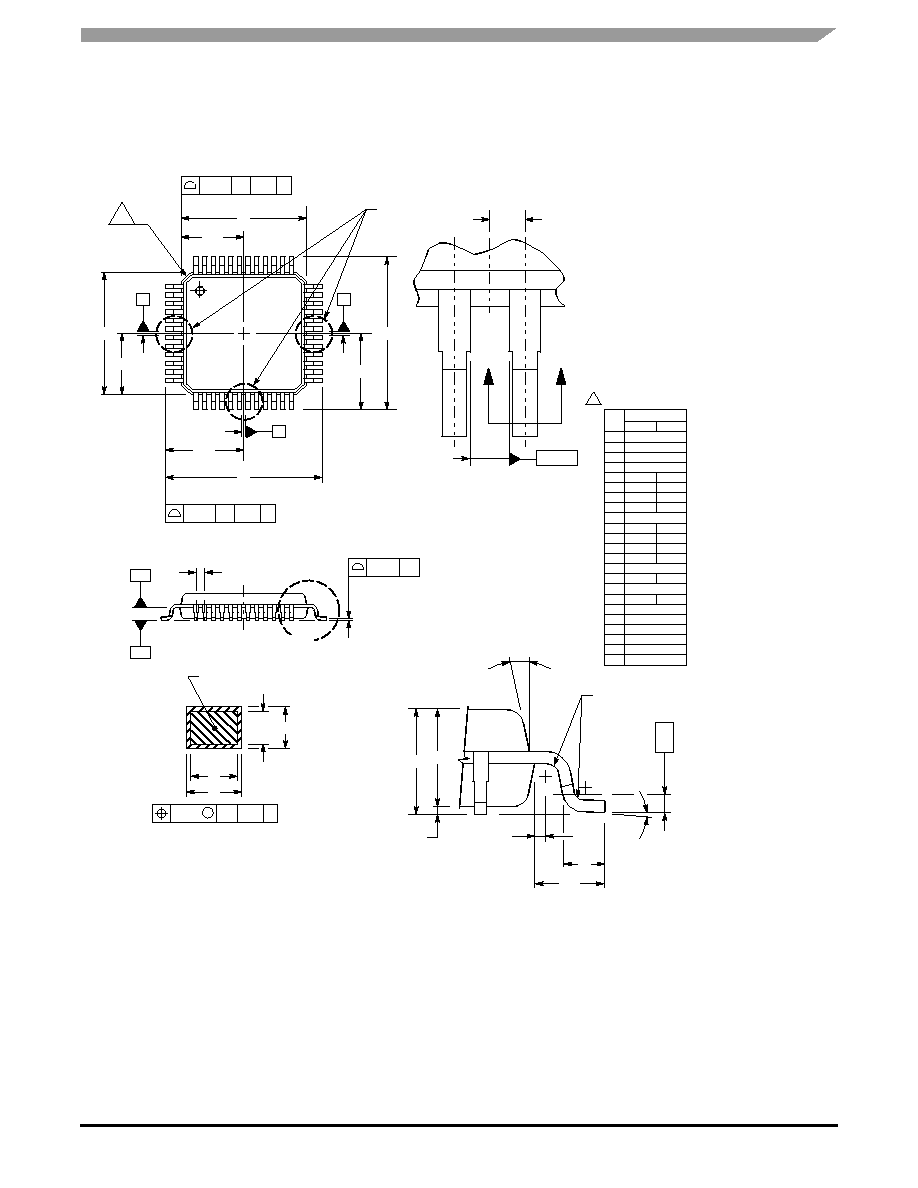
OUTLINE DIMENSIONS
NOTES:
1.
2.
3.
4.
5.
6.
7.
8.
9.
DIMENSIONING AND TOLERANCING PER ASME
Y14.5m, 1994.
CONTROLLING DIMENSION: MILLIMETER.
DATUM PLAN AB IS LOCATED AT BOTTOM OF
LEAD AND IS COINCIDENT WITH THE LEAD
WHERE THE LEAD EXITS THE PLASTIC BODY AT
THE BOTTOM OF THE PARTING LINE.
DATUMS T, U, AND Z TO BE DETERMINED AT
DATAUM PLANE AB.
DIMENSIONS S AND V TO BE DETERMINED AT
SEATING PLANE AC.
DIMENSIONS A AND B DO NOT INCLUDE MOLD
PROTRUSION. ALLOWABLE PROTRUSION IS
0.250 PER SIDE. DIMENSIONS A AND B DO
INCLUDE MOLD MISMATCH AND ARE
DETERMINED AT DATUM PLANE AB.
DIMENSION D DOES NOT INCLUDE DAMBAR
PROTRUSION. DAMBAR PROTRUSION SHALL
NOT CAUSE THE D DIMENSION TO EXCEED
0.350.
MINIMUM SOLDER PLATE THICKNESS SHALL BE
0.0076.
EXACT SHAPE OF EACH CORNER IS OPTIONAL.
A
A1
Z
0.200 AB T-U
4X
Z
0.200 AC T-U
4X
B
B1
1
12
13
24
25
36
37
48
S1
S
V
V1
DETAIL Y
9
T
U
Z
P
AE
AE
T, U, Z
DETAIL Y
M∞
TOP & BOTTOM
L∞
W
K
AA
E
C
H
0.250
R
DETAIL AD
GA
UGE PLANE
AD
G
0.080 AC
AB
AC
BASE METAL
N
J
F
D
T-U
M
0.080
Z
AC
SECTION AE-AE
MIN
1.400
0.170
1.350
0.170
0.050
0.090
0.500
0.090
0∞
0.150
MAX
1.600
0.270
1.450
0.230
0.150
0.200
0.700
0.160
7∞
0.250
DIM
A
A1
B
B1
C
D
E
F
G
H
J
K
M
N
P
L
R
S
S1
V
V1
W
AA
MILLIMETERS
7.000 BSC
3.500 BSC
7.000 BSC
3.500 BSC
0.500 BSC
12∞ REF
0.250 BSC
9.000 BSC
4.500 BSC
9.000 BSC
4.500 BSC
0.200 REF
1.000 REF
FA SUFFIX
48-LEAD LQFP PACKAGE
CASE 932-03
ISSUE F

How to Reach Us:
Home Page:
www.freescale.com
E-mail:
support@freescale.com
USA/Europe or Locations Not Listed:
Freescale Semiconductor
Technical Information Center, CH370
1300 N. Alma School Road
Chandler, Arizona 85224
+1-800-521-6274 or +1-480-768-2130
support@freescale.com
Europe, Middle East, and Africa:
Freescale Halbleiter Deutschland GmbH
Technical Information Center
Schatzbogen 7
81829 Muenchen, Germany
+44 1296 380 456 (English)
+46 8 52200080 (English)
+49 89 92103 559 (German)
+33 1 69 35 48 48 (French)
support@freescale.com
Japan:
Freescale Semiconductor Japan Ltd.
Headquarters
ARCO Tower 15F
1-8-1, Shimo-Meguro, Meguro-ku,
Tokyo 153-0064
Japan
0120 191014 or +81 3 5437 9125
support.japan@freescale.com
Asia/Pacific:
Freescale Semiconductor Hong Kong Ltd.
Technical Information Center
2 Dai King Street
Tai Po Industrial Estate
Tai Po, N.T., Hong Kong
+800 2666 8080
support.asia@freescale.com
For Literature Requests Only:
Freescale Semiconductor Literature Distribution Center
P.O. Box 5405
Denver, Colorado 80217
1-800-441-2447 or 303-675-2140
Fax: 303-675-2150
LDCForFreescaleSemiconductor@hibbertgroup.com
MPC92433
Rev. 2
06/2005
Information in this document is provided solely to enable system and software
implementers to use Freescale Semiconductor products. There are no express or
implied copyright licenses granted hereunder to design or fabricate any integrated
circuits or integrated circuits based on the information in this document.
Freescale Semiconductor reserves the right to make changes without further notice to
any products herein. Freescale Semiconductor makes no warranty, representation or
guarantee regarding the suitability of its products for any particular purpose, nor does
Freescale Semiconductor assume any liability arising out of the application or use of any
product or circuit, and specifically disclaims any and all liability, including without
limitation consequential or incidental damages. "Typical" parameters that may be
provided in Freescale Semiconductor data sheets and/or specifications can and do vary
in different applications and actual performance may vary over time. All operating
parameters, including "Typicals", must be validated for each customer application by
customer's technical experts. Freescale Semiconductor does not convey any license
under its patent rights nor the rights of others. Freescale Semiconductor products are
not designed, intended, or authorized for use as components in systems intended for
surgical implant into the body, or other applications intended to support or sustain life,
or for any other application in which the failure of the Freescale Semiconductor product
could create a situation where personal injury or death may occur. Should Buyer
purchase or use Freescale Semiconductor products for any such unintended or
unauthorized application, Buyer shall indemnify and hold Freescale Semiconductor and
its officers, employees, subsidiaries, affiliates, and distributors harmless against all
claims, costs, damages, and expenses, and reasonable attorney fees arising out of,
directly or indirectly, any claim of personal injury or death associated with such
unintended or unauthorized use, even if such claim alleges that Freescale
Semiconductor was negligent regarding the design or manufacture of the part.
FreescaleTM and the Freescale logo are trademarks of Freescale Semiconductor, Inc.
All other product or service names are the property of their respective owners.
© Freescale Semiconductor, Inc. 2005. All rights reserved.