 | –≠–ª–µ–∫—Ç—Ä–æ–Ω–Ω—ã–π –∫–æ–º–ø–æ–Ω–µ–Ω—Ç: MPC9773FA | –°–∫–∞—á–∞—Ç—å:  PDF PDF  ZIP ZIP |

MPC9773
Rev 5, 08/2005
Freescale Semiconductor
Technical Data
© Freescale Semiconductor, Inc., 2005. All rights reserved.
3.3 V 1:12 LVCMOS PLL Clock
Generator
The MPC9773 is a 3.3 V compatible, 1:12 PLL based clock generator targeted
for high-performance low-skew clock distribution in mid-range to high-
performance networking, computing, and telecom applications. With output
frequencies up to 240 MHz and output skews less than 250 ps the device meets
the needs of the most demanding clock applications.
Features
∑
1:12 PLL based low-voltage clock generator
∑
3.3 V power supply
∑
Internal power-on reset
∑
Generates clock signals up to 242.5 MHz
∑
Maximum output skew of 250 ps
∑
Differential PECL reference clock input
∑
Two LVCMOS PLL reference clock inputs
∑
External PLL feedback supports zero-delay capability
∑
Various feedback and output dividers (refer to Application Section)
∑
Supports up to three individual generated output clock frequencies
∑
Synchronous output clock stop circuitry for each individual output for power
down support
∑
Drives up to 24 clock lines
∑
Ambient temperature range -40
∞C to +85∞C
∑
Pin and function compatible to the MPC973
∑
52-lead Pb-free package available
Functional Description
The MPC9773 utilizes PLL technology to frequency lock its outputs onto an input reference clock. Normal operation of the
MPC9773 requires the connection of the PLL feedback output QFB to feedback input FB_IN to close the PLL feedback path. The
reference clock frequency and the divider for the feedback path determine the VCO frequency. Both must be selected to match
the VCO frequency range. The MPC9773 features an extensive level of frequency programmability between the 12 outputs as
well as the output to input relationships, for instance 1:1, 2:1, 3:1, 3:2, 4:1, 4:3, 5:1, 5:2, 5:3, 5:4, 5:6, 6:1, 8:1 and 8:3.
The QSYNC output will indicate when the coincident rising edges of the above relationships will occur. The selectability of the
feedback frequency is independent of the output frequencies. This allows for very flexible programming of the input reference
versus output frequency relationship. The output frequencies can be either odd or even multiples of the input reference. In addi-
tion, the output frequency can be less than the input frequency for applications where a frequency needs to be reduced by a non-
binary factor. The MPC9773 also supports the 180
∞ phase shift of one of its output banks with respect to the other output banks.
The QSYNC outputs reflect the phase relationship between the QA and QC outputs and can be used for the generation of system
baseline timing signals.
The REF_SEL pin selects the LVPECL or the LVCMOS compatible inputs as the reference clock signal. Two alternative
LVCMOS compatible clock inputs are provided for clock redundancy support. The PLL_EN control selects the PLL bypass con-
figuration for test and diagnosis. In this configuration, the selected input reference clock is routed directly to the output dividers,
bypassing the PLL. The PLL bypass is fully static and the minimum clock frequency specification and all other PLL characteristics
do not apply.
The outputs can be individually disabled (stopped in logic low state) by programming the serial CLOCK_STOP interface of the
MPC9773. The MPC9773 has an internal power-on reset.
The MPC9773 is fully 3.3 V compatible and requires no external loop filter components. All inputs (except PCLK) accept
LVCMOS signals while the outputs provide LVCMOS compatible levels with the capability to drive terminated 50
transmission
lines. For series terminated transmission lines, each of the MPC9773 outputs can drive one or two traces, giving the devices an
effective fanout of 1:24. The device is pin and function compatible to the MPC973 and is packaged in a 52-lead LQFP package.
AE SUFFIX
52-LEAD LQFP PACKAGE
Pb-FREE PACKAGE
CASE 848D-03
FA SUFFIX
52-LEAD LQFP PACKAGE
CASE 848D-03
MPC9773
3.3 V 1:12 LVCMOS
PLL CLOCK GENERATOR
Advanced Clock Drivers Device Data
2
Freescale Semiconductor
MPC9773
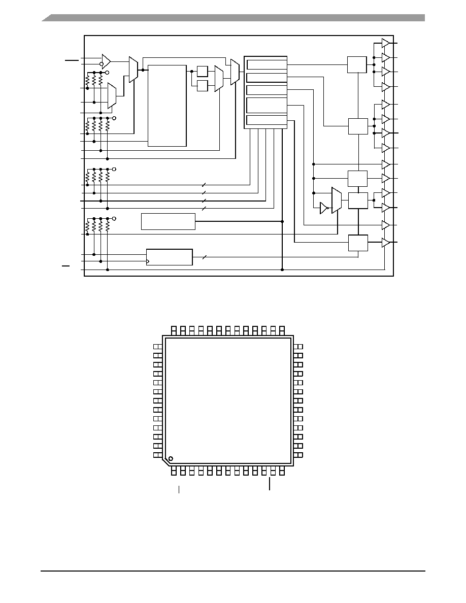
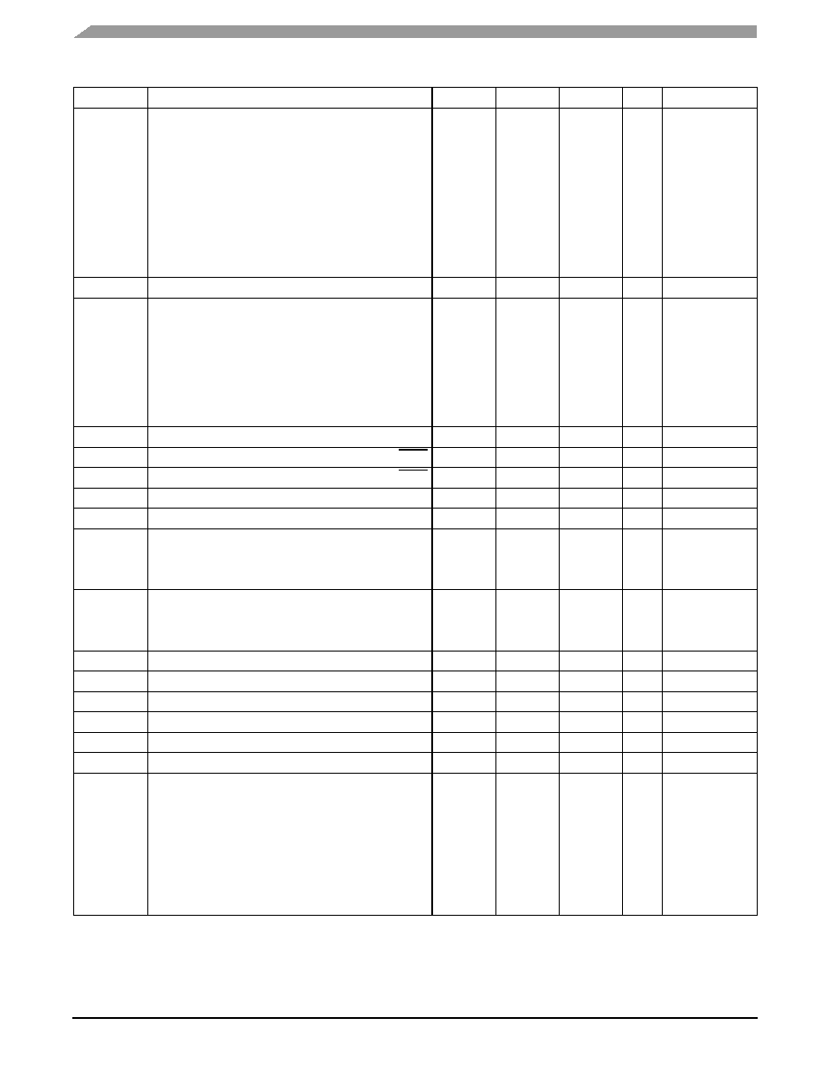
Figure 1. MPC9773 Logic Diagram
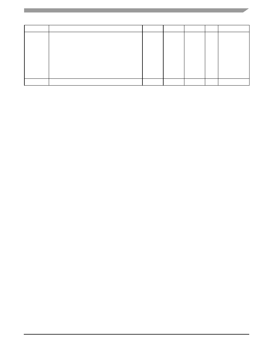
Figure 2. MPC9773 52-Lead Package Pinout (Top View)
PLL
˜4, ˜6, ˜8, ˜12
0
1
1
0
1
0
1
0
QFB
QSYNC
12
3
2
2
2
All input resistors have a value of 25 k
1
0
PCLK
PCLK
CCLK0
CCLK1
FSEL_A[0:1]
FSEL_B[0:1]
FSEL_C[0:1]
INV_CLK
QA0
QA1
QA2
QA3
QB0
QB1
QB2
QB3
QC0
QC1
Bank A
Bank B
Bank C
Clock Stop
VCO
Ref
FB
SYNC PULSE
˜4, ˜6, ˜8, ˜10
˜12, ˜16, ˜20
˜2, ˜4, ˜6, ˜8
˜4, ˜6, ˜8, ˜10
QC2
QC3
FSEL_FB[0:2]
STOP_DATA
STOP_CLK
MR/OE
CCLK_SEL
REF_SEL
FB_IN
VCO_SEL
PLL_EN
V
CC
200≠485 MHz
CLK
Stop
CLK
Stop
CLK
Stop
CLK
Stop
CLK
Stop
V
CC
V
CC
V
CC
˜2
˜1
Power-On Reset
FSEL_B1
FSEL_B0
FSEL_A1
FSEL_A0
QA3
V
CC
QA2
GND
QA1
V
CC
QA0
GND
VCO_SEL
FSEL_FB1
QSYNC
GND
QC0
V
CC
QC1
FSEL_C0
FSEL_C1
QC2
V
CC
QC3
GND
INV_CLK
GND
QB0
V
CC
QB1
GND
QB2
V
CC
QB3
FB
_
I
N
GND
QF
B
V
CC
F
SEL_FB
0
GND
MR
/OE
STOP_C
LK
STOP_DA
T
A
F
SEL_F
B2
PLL_
EN
REF_S
E
L
CCLK_S
E
L
CCL
K0
CCL
K1
V
CC_PLL
PC
LK
PC
LK
40
41
42
43
44
45
46
47
48
49
50
51
52
25
24
23
22
21
20
19
18
17
16
15
14
1 2 3 4 5 6 7 8 9 10 11 12 13
39 38 37 36 35 34 33 32 31 30 29 28 27
26
MPC9773
Advanced Clock Drivers Device Data
Freescale Semiconductor
3
MPC9773
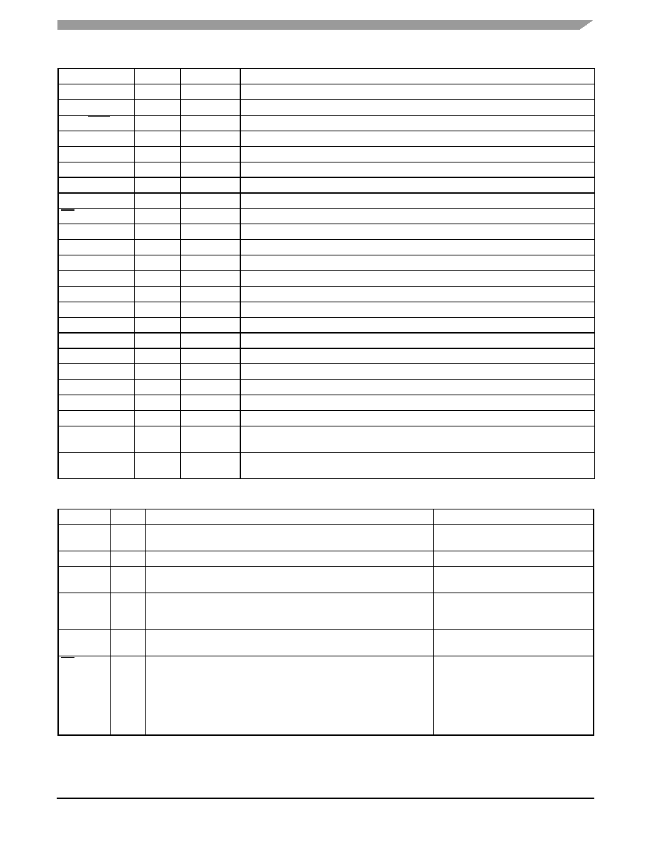
Table 1. Pin Configuration
Pin
I/O
Type
Function
CCLK0
Input
LVCMOS
PLL reference clock
CCLK1
Input
LVCMOS
Alternative PLL reference clock
PCLK, PCLK
Input
LVPECL
Differential LVPECL reference clock
FB_IN
Input
LVCMOS
PLL feedback signal input, connect to an QFB
CCLK_SEL
Input
LVCMOS
LVCMOS clock reference select
REF_SEL
Input
LVCMOS
LVCMOS/PECL reference clock select
VCO_SEL
Input
LVCMOS
VCO operating frequency select
PLL_EN
Input
LVCMOS
PLL enable/PLL bypass mode select
MR/OE
Input
LVCMOS
Output enable/disable (high-impedance tristate) and device reset
FSEL_A[0:1]
Input
LVCMOS
Frequency divider select for bank A outputs
FSEL_B[0:1]
Input
LVCMOS
Frequency divider select for bank B outputs
FSEL_C[0:1]
Input
LVCMOS
Frequency divider select for bank C outputs
FSEL_FB[0:2]
Input
LVCMOS
Frequency divider select for the QFB output
INV_CLK
Input
LVCMOS
Clock phase selection for outputs QC2 and QC3
STOP_CLK
Input
LVCMOS
Clock input for clock stop circuitry
STOP_DATA
Input
LVCMOS
Configuration data input for clock stop circuitry
QA[0-3]
Output
LVCMOS
Clock outputs (Bank A)
QB[0-3]
Output
LVCMOS
Clock outputs (Bank B)
QC[0-3]
Output
LVCMOS
Clock outputs (Bank C)
QFB
Output
LVCMOS
PLL feedback output. Connect to FB_IN.
QSYNC
Output
LVCMOS
Synchronization pulse output
GND
Supply
Ground
Negative power supply
V
CC_PLL
Supply
V
CC
PLL positive power supply (analog power supply). It is recommended to use an external RC
filter for the analog power supply pin V
CC_PLL
. Please refer to applications section for details.
V
CC
Supply
V
CC
Positive power supply for I/O and core. All V
CC
pins must be connected to the positive power
supply for correct operation
Table 2. Function Table (Configuration Controls)
Control
Default
0
1
REF_SEL
1
Selects CCLKx as the PLL reference clock
Selects the LVPECL inputs as the PLL
reference clock
CCLK_SEL
1
Selects CCLK0
Selects CCLK1
VCO_SEL
1
Selects VCO
˜ 2. The VCO frequency is scaled by a factor of 2 (low VCO
frequency range).
Selects VCO
˜ 1 (high VCO frequency
range)
PLL_EN
1
Test mode with the PLL bypassed. The reference clock is substituted for the
internal VCO output. MPC9773 is fully static and no minimum frequency limit
applies. All PLL related AC characteristics are not applicable.
Normal operation mode with PLL
enabled.
INV_CLK
1
QC2 and QC3 are in phase with QC0 and QC1
QC2 and QC3 are inverted (180∞ phase
shift) with respect to QC0 and QC1
MR/OE
1
Outputs disabled (high-impedance state) and device is reset. During reset/
output disable the PLL feedback loop is open and the internal VCO is tied to
its lowest frequency. The MPC9773 requires reset after any loss of PLL lock.
Loss of PLL lock may occur when the external feedback path is interrupted.
The length of the reset pulse should be greater than one reference clock
cycle (CCLKx). The device is reset by the internal power-on reset (POR)
circuitry during power-up.
Outputs enabled (active)
VCO_SEL, FSEL_A[0:1], FSEL_B[0:1], FSEL_C[0:1], FSEL_FB[0:2] control the operating PLL frequency range and input/output frequency
ratios. See
Table 3
to
Table 6
and the Applications Section for supported frequency ranges and output to input frequency ratios.
Advanced Clock Drivers Device Data
4
Freescale Semiconductor
MPC9773
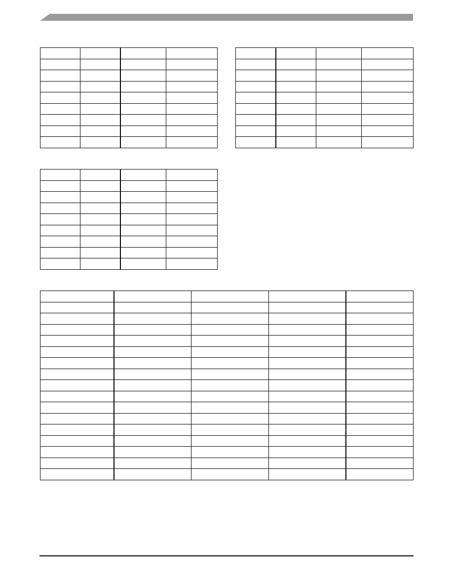
Table 3. Output Divider Bank A (N
A
)
VCO_SEL
FSEL_A1
FSEL_A0
QA[0:3]
0
0
0
VCO
˜ 8
0
0
1
VCO
˜ 12
0
1
0
VCO
˜ 16
0
1
1
VCO
˜ 24
1
0
0
VCO
˜ 4
1
0
1
VCO
˜ 6
1
1
0
VCO
˜ 8
1
1
1
VCO
˜ 12
Table 4. Output Divider Bank B (N
B
)
VCO_SEL
FSEL_B1
FSEL_B0
QB[0:3]
0
0
0
VCO
˜ 8
0
0
1
VCO
˜ 12
0
1
0
VCO
˜ 16
0
1
1
VCO
˜ 20
1
0
0
VCO
˜ 4
1
0
1
VCO
˜ 6
1
1
0
VCO
˜ 8
1
1
1
VCO
˜ 10
Table 5. Ouput Divider Bank C (N
C
)
VCO_SEL
FSEL_C1
FSEL_C0
QC[0:3]
0
0
0
VCO
˜ 4
0
0
1
VCO
˜ 8
0
1
0
VCO
˜ 12
0
1
1
VCO
˜ 16
1
0
0
VCO
˜ 2
1
0
1
VCO
˜ 4
1
1
0
VCO
˜ 6
1
1
1
VCO
˜ 8
Table 6. Output Divider PLL Feedback (M)
VCO_SEL
FSEL_FB2
FSEL_FB1
FSEL_FB0
QFB
0
0
0
0
VCO
˜ 8
0
0
0
1
VCO
˜ 12
0
0
1
0
VCO
˜ 16
0
0
1
1
VCO
˜ 20
0
1
0
0
VCO
˜ 16
0
1
0
1
VCO
˜ 24
0
1
1
0
VCO
˜ 32
0
1
1
1
VCO
˜ 40
1
0
0
0
VCO
˜ 4
1
0
0
1
VCO
˜ 6
1
0
1
0
VCO
˜ 8
1
0
1
1
VCO
˜ 10
1
1
0
0
VCO
˜ 8
1
1
0
1
VCO
˜ 12
1
1
1
0
VCO
˜ 16
1
1
1
1
VCO
˜ 20
Advanced Clock Drivers Device Data
Freescale Semiconductor
5
MPC9773
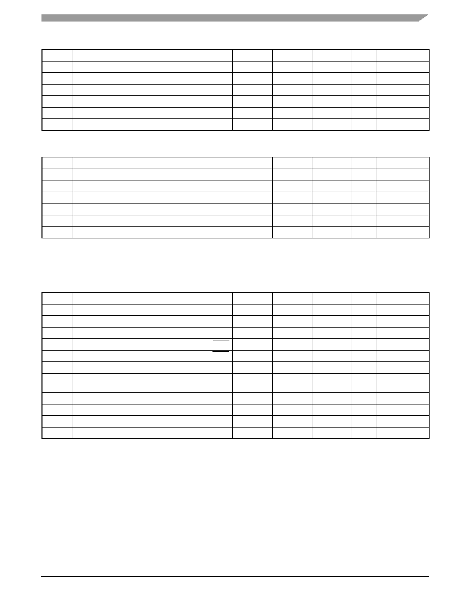
Table 7. General Specifications
Symbol
Characteristics
Min
Typ
Max
Unit
Condition
V
TT
Output Termination Voltage
V
CC
˜ 2
V
MM
ESD Protection (Machine Model)
200
V
HBM
ESD Protection (Human Body Model)
2000
V
LU
Latch-Up Immunity
200
mA
C
PD
Power Dissipation Capacitance
12
pF
Per output
C
IN
Input Capacitance
4.0
pF
Inputs
Table 8. Absolute Maximum Ratings
(1)
1. Absolute maximum continuous ratings are those maximum values beyond which damage to the device may occur. Exposure to these
conditions or conditions beyond those indicated may adversely affect device reliability. Functional operation at absolute-maximum-rated
conditions is not implied.
Symbol
Characteristics
Min
Max
Unit
Condition
V
CC
Supply Voltage
≠0.3
3.9
V
V
IN
DC Input Voltage
≠0.3
V
CC
+ 0.3
V
V
OUT
DC Output Voltage
≠0.3
V
CC
+ 0.3
V
I
IN
DC Input Current
±20
mA
I
OUT
DC Output Current
±50
mA
T
S
Storage Temperature
≠65
125
∞C
Table 9. DC Characteristics (V
CC
= 3.3 V ± 5%, T
A
= -40∞C to 85∞C)
Symbol
Characteristics
Min
Typ
Max
Unit
Condition
V
CC_PLL
PLL Supply Voltage
3.0
V
CC
V
LVCMOS
V
IH
Input High Voltage
2.0
V
CC
+ 0.3
V
LVCMOS
V
IL
Input Low Voltage
0.8
V
LVCMOS
V
PP
Peak-to-Peak Input Voltage
PCLK, PCLK
250
mV
LVPECL
V
CMR
Common Mode Range
(1)
PCLK, PCLK
1. V
CMR
(DC) is the crosspoint of the differential input signal. Functional operation is obtained when the crosspoint is within the V
CMR
range
and the input swing lies within the V
PP
(DC) specification.
1.0
V
CC
≠ 0.6
V
LVPECL
V
OH
Output High Voltage
2.4
V
I
OH
= ≠24 mA
(2)
2. The MPC9773 is capable of driving 50
transmission lines on the incident edge. Each output drives one 50 parallel terminated
transmission line to a termination voltage of V
TT
. Alternatively, the device drives up to two 50
series terminated transmission lines.
V
OL
Output Low Voltage
0.55
0.30
V
V
I
OL
= 24 mA
I
OL
= 12 mA
Z
OUT
Output Impedance
14 ≠ 17
I
IN
Input Current
(3)
3. Inputs have pull-down resistors affecting the input current.
±200
µA
V
IN
= V
CC
or GND
I
CC_PLL
Maximum PLL Supply Current
8.0
13.5
mA
V
CC_PLL
Pin
I
CCQ
Maximum Quiescent Supply Current
35
mA
All V
CC
Pins
Advanced Clock Drivers Device Data
6
Freescale Semiconductor
MPC9773
Table 10. AC Characteristics (V
CC
= 3.3 V ± 5%, T
A
= -40∞C to 85∞C)
(1),
(2)
Symbol
Characteristics
Min
Typ
Max
Unit
Condition
f
REF
Input Reference Frequency
˜ 4 feedback
˜ 6 feedback
˜ 8 feedback
˜ 10 feedback
˜ 12 feedback
˜ 16 feedback
˜ 20 feedback
˜ 24 feedback
˜ 32 feedback
˜ 40 feedback
Input Reference Frequency in PLL Bypass Mode
50.0
33.3
25.0
20.0
16.6
12.5
10.0
8.33
6.25
5.00
121.2
80.8
60.6
48.5
40.4
30.3
24.2
20.2
15.1
12.1
250
MHz
MHz
MHz
MHz
MHz
MHz
MHz
MHz
MHz
MHz
MHz
PLL locked
PLL bypass
f
VCO
VCO Frequency Range
200
485
MHz
f
MAX
Output Frequency
˜ 2 output
˜ 4 output
˜ 6 output
˜ 8 output
˜ 10 output
˜ 12 output
˜ 16 output
˜ 20 output
˜ 24 output
100.0
50.0
33.3
25.0
20.0
16.6
12.5
10.0
8.33
242.5
121.2
80.8
60.6
48.5
40.4
30.3
24.2
20.2
MHz
MHz
MHz
MHz
MHz
MHz
MHz
MHz
MHz
PLL locked
f
STOP_CLK
Serial Interface Clock Frequency
20
MHz
V
PP
Peak-to-Peak Input Voltage
PCLK, PCLK
400
1000
mV
LVPECL
V
CMR
Common Mode Range
(3)
PCLK, PCLK
1.2
V
CC
≠ 0.9
V
LVPECL
t
PW,MIN
Input Reference Pulse Width
(4)
2.0
ns
t
R
, t
F
CCLKx Input Rise/Fall Time
(5)
1.0
ns
0.8 to 2.0 V
t
(
)
Propagation Delay (static phase offset)
(6)
6.25 MHz < f
REF
< 65.0 MHz
65.0 MHz < f
REF
< 125 MHz
f
REF
= 50 MHz and feedback =
˜8
≠3
≠4
≠166
+3
+4
+166
∞
∞
ps
PLL locked
t
SK(O)
Output-to-Output Skew
(7)
within QA outputs
within QB outputs
within QC outputs
all outputs
100
100
100
250
ps
ps
ps
ps
DC
Output Duty Cycle
(8)
(T
˜2) ≠200
T
˜2
(T
˜2) +200
ps
t
R
, t
F
Output Rise/Fall Time
0.1
1.0
ns
0.55 to 2.4 V
t
PLZ, HZ
Output Disable Time
8.0
ns
t
PZL, LZ
Output Enable Time
8.0
ns
t
JIT(CC)
Cycle-to-cycle Jitter
(9)
150
ps
t
JIT(PER)
Period Jitter
(10)
100
ps
t
JIT(
)
I/O Phase Jitter RMS (1
)
(11)
˜ 4 feedback
˜ 6 feedback
˜ 8 feedback
˜ 10 feedback
˜ 12 feedback
˜ 16 feedback
˜ 20 feedback
˜ 24 feedback
˜ 32 feedback
˜ 40 feedback
11
86
13
88
16
19
21
22
27
30
ps
ps
ps
ps
ps
ps
ps
ps
ps
ps
(VCO = 400 MHz)
Advanced Clock Drivers Device Data
Freescale Semiconductor
7
MPC9773
BW
PLL Closed Loop Bandwidth
(12)
˜ 4 feedback
˜ 6 feedback
˜ 8 feedback
˜ 10 feedback
˜ 12 feedback
˜ 16 feedback
˜ 20 feedback
˜ 24 feedback
˜ 32 feedback
˜ 40 feedback
1.20 ≠ 3.50
0.70 ≠ 2.50
0.50 ≠ 1.80
0.45 ≠ 1.20
0.30 ≠ 1.00
0.25 ≠ 0.70
0.20 ≠ 0.55
0.17 ≠ 0.40
0.12 ≠ 0.30
0.11 ≠ 0.28
MHz
MHz
MHz
MHz
MHz
MHz
MHz
MHz
MHz
MHz
t
LOCK
Maximum PLL Lock Time
10
ms
1. AC characteristics apply for parallel output termination of 50
to V
TT
.
2. The input reference frequency must match the VCO lock range divided by the feedback divider ratio: f
REF
= f
VCO
˜ (M VCO_SEL).
3. V
CMR
(AC) is the crosspoint of the differential input signal. Normal AC operation is obtained when the crosspoint is within the V
CMR
range
and the input swing lies within the V
PP
(AC) specification. Violation of V
CMR
or V
PP
impacts static phase offset t
(
)
.
4. Calculation of reference duty cycle limits: DC
REF,MIN
= t
PW,MIN
f
REF
100% and DC
REF,MAX
= 100% ≠ DC
REF,MIN
.
5. The MPC9773 will operate with input rise/fall times up to 3.0 ns, but the AC characteristics, specifically t
(
)
, t
PW,MIN
, DC and f
MAX
can only
be guaranteed if t
R
, t
F
are within the specified range.
6. CCLKx or PCLK to FB_IN. Static phase offset depends on the reference frequency. t
(
)
[s] = t
(
)
[
∞] ˜ (f
REF
360∞).
7. Excluding QSYNC output. Refer to
APPLICATIONS INFORMATION
for part-to-part skew calculation.
8. Output duty cycle is DC = (0.5
± 200 ps f
OUT
)
100%. E.g., the DC range at f
OUT
= 100 MHz is 48% < DC < 52%. T = output period.
9. Cycle jitter is valid for all outputs in the same divider configuration.
10. Period jitter is valid for all outputs in the same divider configuration.
11. I/O jitter is valid for a VCO frequency of 400 MHz. Refer to
APPLICATIONS INFORMATION
for I/O jitter vs. VCO frequency.
12. ≠3 dB point of PLL transfer characteristics.
Table 10. AC Characteristics (V
CC
= 3.3 V ± 5%, T
A
= -40∞C to 85∞C)
(1),
(2)
Symbol
Characteristics
Min
Typ
Max
Unit
Condition
Advanced Clock Drivers Device Data
8
Freescale Semiconductor
MPC9773
APPLICATIONS INFORMATION
MPC9773 Configurations
Configuring the MPC9773 amounts to properly configuring
the internal dividers to produce the desired output
frequencies. The output frequency can be represented by
this formula:
where f
REF
is the reference frequency of the selected input
clock source (CCLKO, CCLK1 or PCLK), M is the PLL
feedback divider and N is an output divider. The PLL
feedback divider is configured by the FSEL_FB[2:0] and the
output dividers are individually configured for each output
bank by the FSEL_A[1:0], FSEL_B[1:0] and FSEL_C[1:0]
inputs.
The reference frequency f
REF
and the selection of the
feedback-divider M is limited by the specified VCO frequency
range. f
REF
and M must be configured to match the VCO
frequency range of 200 to 480 MHz in order to achieve stable
PLL operation:
f
VCO,MIN
(f
REF
VCO_SEL
M)
f
VCO,MAX
The PLL post-divider VCO_SEL is either a divide-by-one
or a divide-by-two and can be used to situate the VCO into
the specified frequency range. This divider is controlled by
the VCO_SEL pin. VCO_SEL effectively extends the usable
input frequency range while it has no effect on the output to
reference frequency ratio.
The output frequency for each bank can be derived from
the VCO frequency and output divider:
f
QA[0:3]
= f
VCO
˜ (VCO_SEL N
A
)
f
QB[0:3]
= f
VCO
˜ (VCO_SEL N
B
)
f
QC[0:3]
= f
VCO
˜ (VCO_SEL N
C
)
Table 11
shows the various PLL feedback and output
dividers, and
Figure 3
and
Figure 4
display example
configurations for the MPC9773.
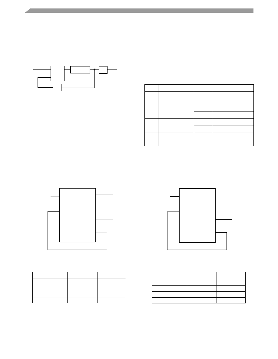
Figure 3. Example Configuration
Figure 4. Example Configuration
˜VCO_SEL
˜M
˜N
f
REF
f
OUT
f
OUT
= f
REF
M ˜ N
PLL
Table 11. MPC9773 Divider
Divider
Function
VCO_SEL
Values
M
PLL Feedback
FSEL_FB[0:3]
˜1
4, 6, 8, 10, 12, 16
˜2
8, 12, 16, 20, 24, 32, 40
N
A
Bank A Output
Divider FSEL_A[0:1]
˜1
4, 6, 8, 12
˜2
8, 12, 16, 24
N
B
Bank B Output
Divider FSEL_B[0:1]
˜1
4, 6, 8, 10
˜2
8, 12, 16, 20
N
C
Bank C Output
Divider FSEL_C[0:1]
˜1
2, 4, 6, 8
˜2
4, 8, 12, 16
MPC9773
f
REF
= 33.3 MHz
33.3 MHz
100 MHz
33.3 MHz (Feedback)
200 MHz
CCLK0
VCO_SEL
FSEL_A[1:0]
FSEL_B[1:0]
FSEL_C[1:0]
FSEL_FB[2:0]
QA[3:0]
QB[3:0]
QC[3:0]
QFB
CCLK1
CCLK_SEL
FB_IN
1
11
00
00
101
MPC9773 example configuration (feedback of
QFB = 33.3 MHz, f
VCO
= 400 MHz, VCO_SEL =
˜1,
M = 12, N
A
= 12, N
B
= 4, N
C
= 2).
Frequency Range
Min
Max
Input
16.6 MHz
40 MHz
QA outputs
16.6 MHz
40 MHz
QB outputs
50 MHz
120 MHz
QC outputs
100 MHz
240 MHz
MPC9773
f
REF
= 25 MHz
62.5 MHz
62.5 MHz
25 MHz (Feedback)
125 MHz
CCLK0
VCO_SEL
FSEL_A[1:0]
FSEL_B[1:0]
FSEL_C[1:0]
FSEL_FB[2:0]
QA[3:0]
QB[3:0]
QC[3:0]
QFB
CCLK1
CCLK_SEL
FB_IN
1
00
00
00
011
MPC9773 example configuration (feedback of
QFB = 25 MHz, f
VCO
= 250 MHz, VCO_SEL =
˜1,
M = 10, N
A
= 4, N
B
= 4, N
C
= 2).
Frequency Range
Min
Max
Input
20 MHz
48 MHz
QA outputs
50 MHz
120 MHz
QB outputs
50 MHz
120 MHz
QC outputs
100 MHz
240 MHz
Advanced Clock Drivers Device Data
Freescale Semiconductor
9
MPC9773
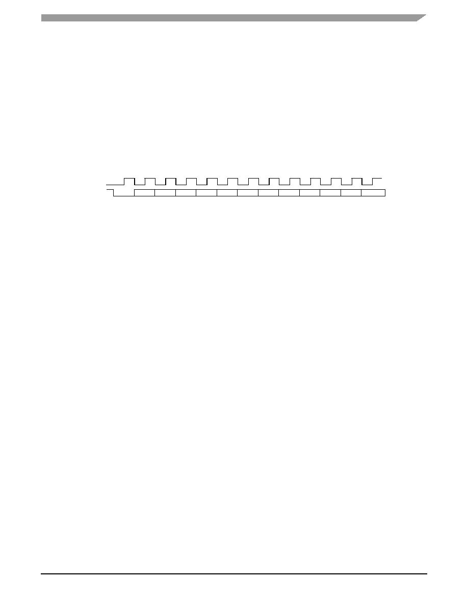
MPC9773 Individual Output Disable (Clock Stop)
Circuitry
The individual clock stop (output enable) control of the
MPC9773 allows designers, under software control, to
implement power management into the clock distribution
design. A simple serial interface and a clock stop control logic
provides a mechanism through which the MPC9773 clock
outputs can be individually stopped in the logic `0' state: The
clock stop mechanism allows serial loading of a 12-bit serial
input register. This register contains one programmable clock
stop bit for 12 of the 14 output clocks. The QC0 and QFB
outputs cannot be stopped (disabled) with the serial port.
The user can program an output clock to stop (disable) by
writing logic `0' to the respective stop enable bit. Likewise, the
user may programmably enable an output clock by writing
logic `1' to the respective enable bit. The clock stop logic
enables or disables clock outputs during the time when the
output would normally be in logic low state, eliminating the
possibility of short or `runt' clock pulses.
The user can write to the serial input register through the
STOP_DATA input by supplying a logic `0' start bit followed
serially by 12 NRZ disable/enable bits. The period of each
STOP_DATA bit equals the period of the free-running
STOP_CLK signal. The STOP_DATA serial transmission
should be timed so the MPC9773 can sample each
STOP_DATA bit with the rising edge of the free-running
STOP_CLK signal. (See
Figure 5
.)
Figure 5. Clock Stop Circuit Programing
STOP_CLK
STOP_DATA
START
QA0
QA1
QA2
QA3
QB0
QB1
QB2
QB3
QC1
QC2
QC3
QSYNC
Advanced Clock Drivers Device Data
10
Freescale Semiconductor
MPC9773
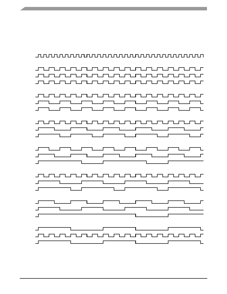
SYNC Output Description
The MPC9773 has a system synchronization pulse output
QSYNC. In configurations for which the output frequency
relationships are not integer multiples of each other, QSYNC
provides a signal for system synchronization purposes. The
MPC9773 monitors the relationship between the A bank and
the B bank of outputs. The QSYNC output is asserted (logic
low) one period in duration and one period prior to the
coincident rising edges of the QA and QC outputs. The
duration and the placement of the pulse is dependent on QA
and QC output frequencies: the QSYNC pulse width is equal
to the period of the higher of the QA and QC output
frequencies.
Figure 6
shows various waveforms for the
QSYNC output. The QSYNC output is defined for all possible
combinations of the bank A and bank C outputs.
Figure 6. QSYNC Timing Diagram
f
VCO
1:1 Mode
QA
QC
QSYNC
2:1 Mode
QC(
˜2)
QA(
˜6)
QSYNC
3:1 Mode
QA
QC
QSYNC
QA(
˜4)
QC(
˜6)
QSYNC
3:2 Mode
QC(
˜2)
QA(
˜8)
QSYNC
4:1 Mode
QA(
˜6)
QC(
˜8)
QSYNC
4:3 Mode
QA(
˜12)
QC(
˜2)
QSYNC
6:1 Mode
Advanced Clock Drivers Device Data
Freescale Semiconductor
11
MPC9773
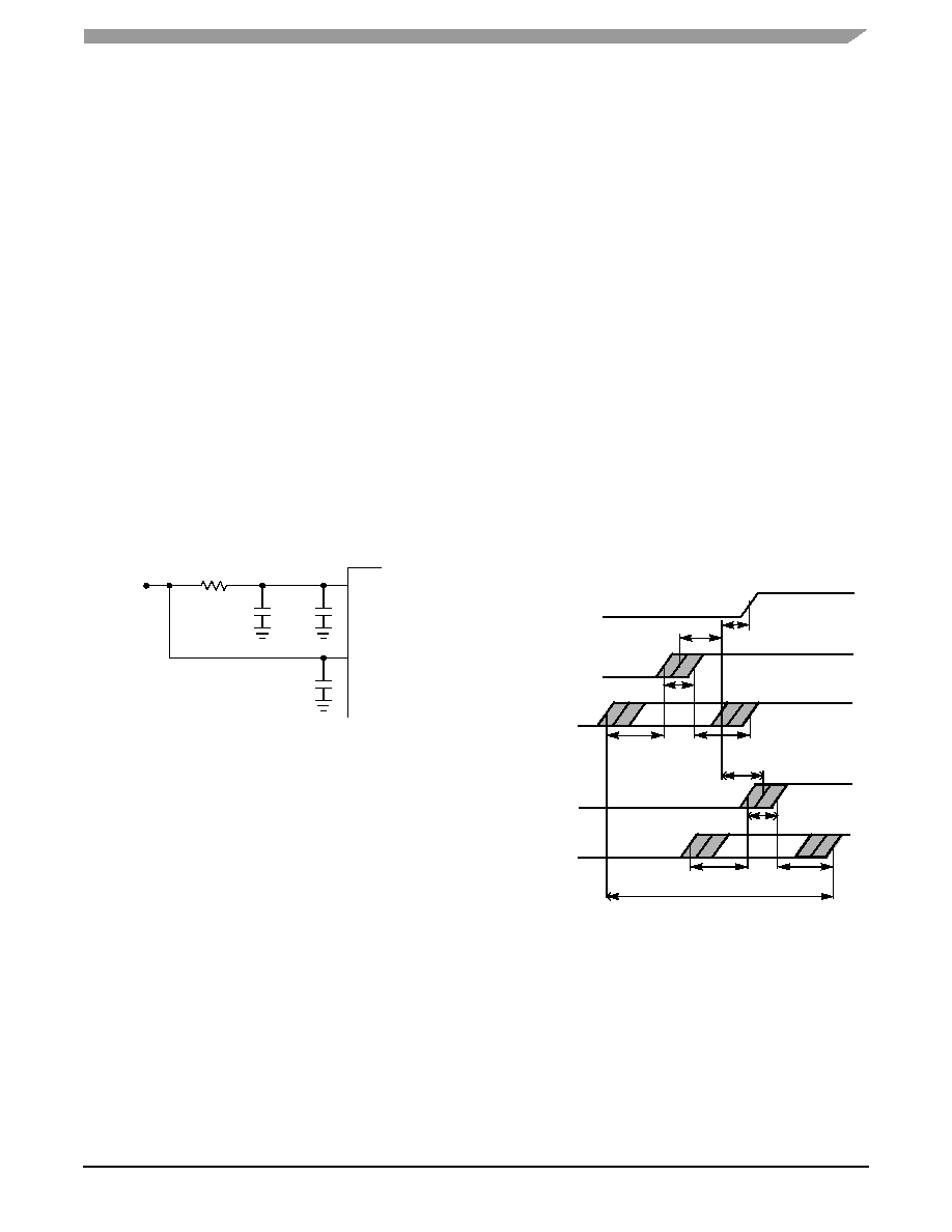
Power Supply Filtering
The MPC9773 is a mixed analog/digital product. Its analog
circuitry is naturally susceptible to random noise, especially if
this noise is seen on the power supply pins. Random noise
on the V
CC_PLL
power supply impacts the device
characteristics, for instance I/O jitter. The MPC9773 provides
separate power supplies for the output buffers (V
CC
) and the
phase-locked loop (V
CC_PLL
) of the device. The purpose of
this design technique is to isolate the high switching noise
digital outputs from the relatively sensitive internal analog
phase-locked loop. In a digital system environment where it
is more difficult to minimize noise on the power supplies, a
second level of isolation may be required. The simple but
effective form of isolation is a power supply filter on the
V
CCA_PLL
pin for the MPC9773.
Figure 7
illustrates a typical
power supply filter scheme. The MPC9773 frequency and
phase stability is most susceptible to noise with spectral
content in the 100-kHz to 20-MHz range. Therefore, the filter
should be designed to target this range. The key parameter
that needs to be met in the final filter design is the DC voltage
drop across the series filter resistor R
F
. From the data sheet
the I
CC_PLL
current (the current sourced through the V
CC_PLL
pin) is typically 8 mA (13.5 mA maximum), assuming that a
minimum of 3.0 V must be maintained on the V
CC_PLL
pin.
The resistor R
F
shown in
Figure 7
must have a resistance of
5≠10
to meet the voltage drop criteria.
Figure 7. V
CC_PLL
Power Supply Filter
The minimum values for R
F
and the filter capacitor C
F
are
defined by the required filter characteristics: the RC filter
should provide an attenuation greater than 40 dB for noise
whose spectral content is above 100 kHz. In the example RC
filter shown in
Figure 7
, the filter cut-off frequency is around
4.5 kHz and the noise attenuation at 100 kHz is better than
42 dB.
As the noise frequency crosses the series resonant point
of an individual capacitor, its overall impedance begins to
look inductive and thus increases with increasing frequency.
The parallel capacitor combination shown ensures that a low
impedance path to ground exists for frequencies well above
the bandwidth of the PLL. Although the MPC9773 has
several design features to minimize the susceptibility to
power supply noise (isolated power and grounds and fully
differential PLL), there still may be applications in which
overall performance is being degraded due to system power
supply noise. The power supply filter schemes discussed in
this section should be adequate to eliminate power supply
noise related problems in most designs.
Using the MPC9773 in Zero-Delay Applications
Nested clock trees are typical applications for the
MPC9773. Designs using the MPC9773 as an LVCMOS PLL
fanout buffer with zero insertion delay will show significantly
lower clock skew than clock distributions developed from
CMOS fanout buffers. The external feedback option of the
MPC9773 clock driver allows for its use as a zero delay
buffer. The PLL aligns the feedback clock output edge with
the clock input reference edge, resulting in a near zero delay
through the device (the propagation delay through the device
is virtually eliminated). The maximum insertion delay of the
device in zero-delay applications is measured between the
reference clock input and any output. This effective delay
consists of the static phase offset, I/O jitter (phase or long-
term jitter), feedback path delay and the output-to-output
skew error relative to the feedback output.
Calculation of Part-to-Part Skew
The MPC9773 zero delay buffer supports applications
where critical clock signal timing can be maintained across
several devices. If the reference clock inputs of two or more
MPC9773 are connected together, the maximum overall
timing uncertainty from the common CCLKx input to any
output is:
t
SK(PP)
= t
(
)
+ t
SK(O)
+ t
PD, LINE(FB)
+ t
JIT(
)
CF
This maximum timing uncertainty consists of 4
components: static phase offset, output skew, feedback
board trace delay, and I/O (phase) jitter:
Figure 8. MPC9773 Maximum Device-to-Device Skew
V
CC_PLL
V
CC
MPC9773
10 nF
R
F
= 5≠10
C
F
33...100 nF
R
F
V
CC
C
F
= 22
µF
t
PD,LINE(FB)
t
JIT(
)
+t
SK(O)
≠t
(
)
+t
(
)
t
JIT(
)
+t
SK(O)
t
SK(PP)
Max. skew
CCLK
Common
QFB
Device 1
Any Q
Device 1
QFB
Device2
Any Q
Device 2

Advanced Clock Drivers Device Data
12
Freescale Semiconductor
MPC9773
Due to the statistical nature of I/O jitter, an RMS value (1
) is specified. I/O jitter numbers for other confidence factors
(CF) can be derived from
Table 12
.
The feedback trace delay is determined by the board
layout and can be used to fine-tune the effective delay
through each device.
Due to the frequency dependence of the static phase
offset and I/O jitter, using
Figure 9
to
Figure 11
to predict a
maximum I/O jitter and the specified t
(
)
parameter relative to
the input reference frequency results in a precise timing
performance analysis.
In the following example calculation an I/O jitter confidence
factor of 99.7% (
± 3) is assumed, resulting in a worst-case
timing uncertainty from the common input reference clock to
any output of ≠455 ps to +455 ps relative to CCLK (PLL
feedback =
˜8, reference frequency = 50 MHz, VCO
frequency = 400 MHz, I/O jitter = 13 ps RMS max., static
phase offset t
(
)
=
± 166 ps):
t
SK(PP)
= [≠166ps...166ps] + [≠250ps...250ps] +
[(13ps
≠3)...(13ps 3)] + t
PD, LINE(FB)
t
SK(PP)
= [≠455ps...455ps] + t
PD, LINE(FB)
Figure 9. MPC9773 I/O Jitter
Figure 10. MPC9773 I/O Jitter
Figure 11. MPC9773 I/O Jitter
Driving Transmission Lines
The MPC9773 clock driver was designed to drive high
speed signals in a terminated transmission line environment.
To provide the optimum flexibility to the user, the output
drivers were designed to exhibit the lowest impedance
possible. With an output impedance of less than 20
, the
drivers can drive either parallel or series terminated
transmission lines. For more information on transmission
lines the reader is referred to Freescale Semiconductor
application note AN1091. In most high-performance clock
networks point-to-point distribution of signals is the method of
choice. In a point-to-point scheme, either series terminated or
parallel terminated transmission lines can be used. The
parallel technique terminates the signal at the end of the line
with a 50-
resistance to V
CC
˜ 2.
Table 12. Confidence Factor CF
CF
Probability of Clock Edge
within the Distribution
± 1
0.68268948
± 2
0.95449988
± 3
0.99730007
± 4
0.99993663
± 5
0.99999943
± 6
0.99999999
VCO frequency [MHz]
200
250
300
350
400
450 480
160
140
120
100
80
60
40
20
0
FB =
˜32
FB =
˜16
FB =
˜8
FB =
˜4
Maximum I/O Phase Jitter versus Frequency Parameter:
PLL Feedback Divider FB
t
ji
t
[
]
[p
s
]
RMS
VCO frequency [MHz]
200
250
300
350
400
450 480
120
100
80
60
40
20
0
FB =
˜12
FB =
˜24
Maximum I/O Phase Jitter versus Frequency Parameter:
PLL Feedback Divider FB
FB =
˜6
t
jit
[
]
[p
s]
RMS
VCO frequency [MHz]
200
250
300
350
400
450
480
140
120
100
80
60
40
20
0
FB =
˜20
FB =
˜10
FB =
˜40
Maximum I/O Phase Jitter versus Frequency Parameter:
PLL Feedback Divider FB
t
ji
t[
]
[p
s]
RMS
Advanced Clock Drivers Device Data
Freescale Semiconductor
13
MPC9773
This technique draws a fairly high level of DC current and
thus only a single terminated line can be driven by each
output of the MPC9773 clock driver. For the series terminated
case, however, there is no DC current draw; thus the outputs
can drive multiple series terminated lines.
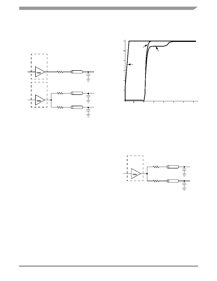
Figure 12
illustrates an output driving a single series terminated line
versus two series terminated lines in parallel. When taken to
its extreme the fanout of the MPC9773 clock driver is
effectively doubled due to its capability to drive multiple lines.
Figure 12. Single versus Dual Transmission Lines
The waveform plots in
Figure 13
show the simulation
results of an output driving a single line versus two lines. In
both cases the drive capability of the MPC9773 output buffer
is more than sufficient to drive 50-
transmission lines on the
incident edge. Note from the delay measurements in the
simulations that a delta of only 43 ps exists between the two
differently loaded outputs. This suggests that the dual line
driving need not be used exclusively to maintain the tight
output-to-output skew of the MPC9773. The output waveform
in
Figure 13
shows a step in the waveform. This step is
caused by the impedance mismatch seen looking into the
driver. The parallel combination of the
36-
series resistor plus the output impedance does not
match the parallel combination of the line impedances. The
voltage wave launched down the two lines will equal:
V
L
= V
S
(Z
0
˜ (R
S
+ R
0
+ Z
0
))
Z
0
= 50
|| 50
R
S
= 36
|| 36
R
0
= 14
V
L
= 3.0 (25
˜ (18+17+25)
= 1.31 V
At the load end the voltage will double, due to the near
unity reflection coefficient, to 2.6 V. It will then increment
towards the quiescent 3.0 V in steps separated by one round
trip delay (in this case 4.0 ns).
1.
Final skew data pending specification.
Figure 13. Single versus Dual Waveforms
Since this step is well above the threshold region it will not
cause any false clock triggering; however, designers may be
uncomfortable with unwanted reflections on the line. To better
match the impedances when driving multiple lines, the
situation in
Figure 14
should be used. In this case the series
terminating resistors are reduced such that when the parallel
combination is added to the output buffer impedance, the line
impedance is perfectly matched.
Figure 14. Optimized Dual Line Termination
14
In
MPC9773
Output
Buffer
R
S
= 36
Z
O
= 50
OutA
14
In
MPC9773
Output
Buffer
R
S
= 36
Z
O
= 50
OutB0
R
S
= 36
Z
O
= 50
OutB1
Time (ns)
Volt
age (V)
3.0
2.5
2.0
1.5
1.0
0.5
0
2
4
6
8
10
12
14
OutB
t
D
= 3.9386
OutA
t
D
= 3.8956
In
14
MPC9773
Output
Buffer
R
S
= 22
Z
O
= 50
R
S
= 22
Z
O
= 50
14
+ 22 || 22 = 50 || 50
25
= 25
Advanced Clock Drivers Device Data
14
Freescale Semiconductor
MPC9773
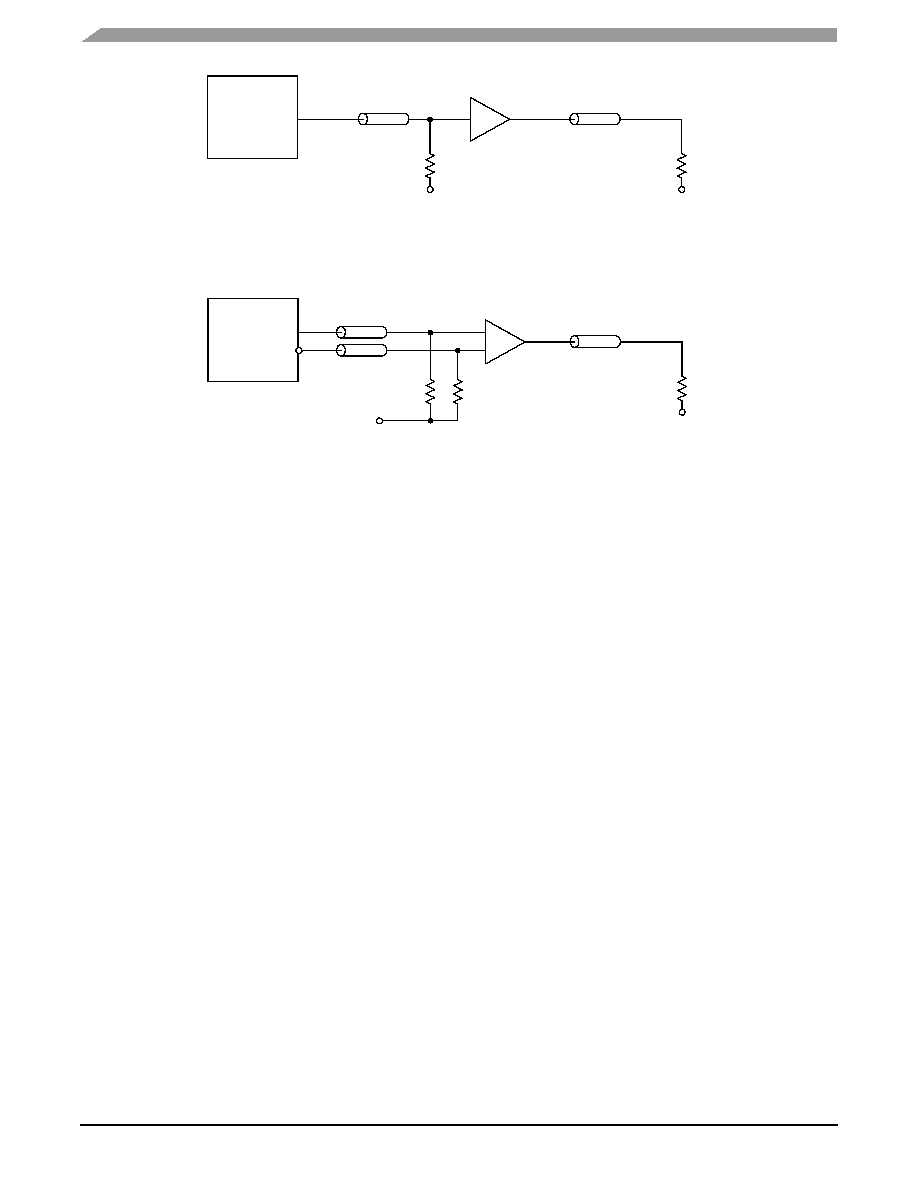
Figure 15. CCLK MPC9773 AC Test Reference
Figure 16. PCLK MPC9773 AC Test Reference
Pulse
Generator
Z = 50
R
T
= 50
Z
O
= 50
R
T
= 50
Z
O
= 50
MPC9773 DUT
V
TT
V
TT
Differential Pulse
Generator
Z = 50
R
T
= 50
Z
O
= 50
R
T
= 50
Z
O
= 50
MPC9773 DUT
V
TT
V
TT
Advanced Clock Drivers Device Data
Freescale Semiconductor
15
MPC9773
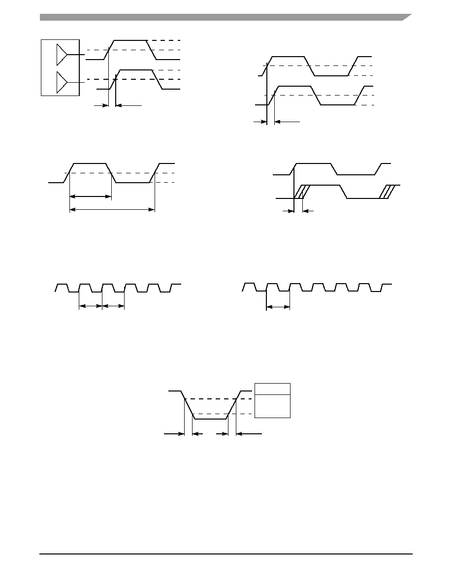
Figure 17. Output-to-Output Skew t
SK(O)
Figure 18. Propagation Delay (t
(
)
, Static Phase
Offset) Test Reference
Figure 19. Output Duty Cycle (DC)
The pin-to-pin skew is defined as the worst case difference in propagation
delay between any similar delay path within a single device
The time from the PLL controlled edge to the non controlled edge,
divided by the time between PLL controlled edges, expressed as
a percentage
V
CC
V
CC
˜ 2
GND
V
CC
V
CC
˜ 2
GND
t
SK(O)
V
CC
V
CC
˜ 2
GND
t
P
T
0
DC = t
P
/T
0
x 100%
V
CC
V
CC
˜ 2
GND
V
CC
V
CC
˜ 2
GND
t
(
)
CCLKx
FB_IN
T
JIT(
)
= |T
0
-T
1
mean|
CCLKx
FB_IN
The deviation in t
0
for a controlled edge with respect to a t
0
mean in a random
sample of cycles
Figure 20. I/O Jitter
T
N
T
JIT(CC)
= |T
N
≠T
N+1
|
T
N+1
T
JIT(PER)
= |T
N
≠1/f
0
|
T
0
Figure 21. Cycle-to-Cycle Jitter
Figure 22. Period Jitter
The variation in cycle time of a signal between adjacent cycles, over a random
sample of adjacent cycle pairs
The deviation in cycle time of a signal with respect to the ideal period over a
random sample of cycles
t
F
t
R
V
CC
= 3.3 V
2.4
0.55
Figure 23. Output Transition Time Test Reference
Advanced Clock Drivers Device Data
16
Freescale Semiconductor
MPC9773
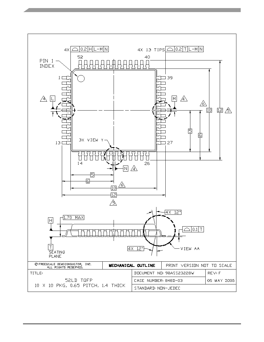
PACKAGE DIMENSIONS
PAGE 1 OF 3
CASE 848D-03
ISSUE F
52-LEAD LQFP PACKAGE
Advanced Clock Drivers Device Data
Freescale Semiconductor
17
MPC9773
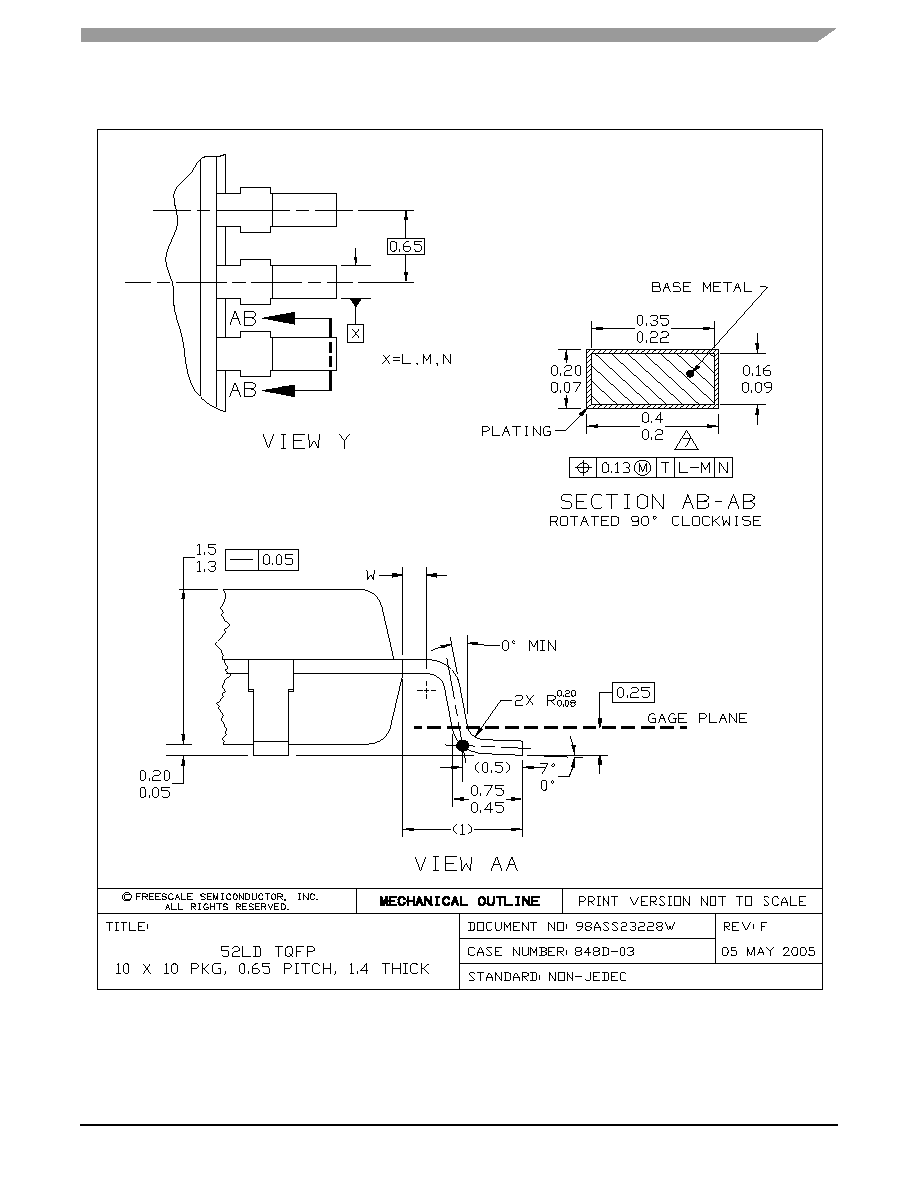
PACKAGE DIMENSIONS
PAGE 2 OF 3
CASE 848D-03
ISSUE F
52-LEAD LQFP PACKAGE
Advanced Clock Drivers Device Data
18
Freescale Semiconductor
MPC9773
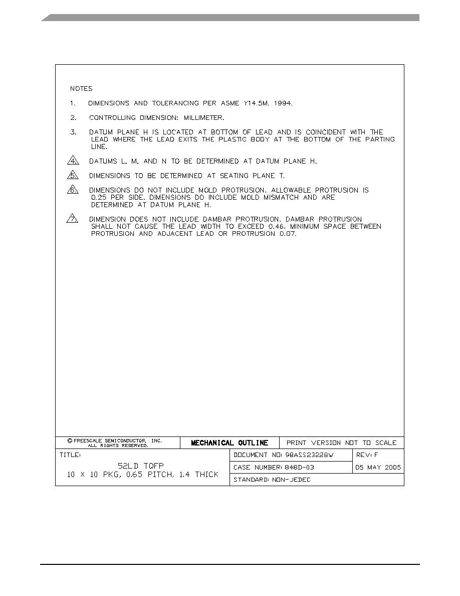
PACKAGE DIMENSIONS
PAGE 3 OF 3
CASE 848D-03
ISSUE F
52-LEAD LQFP PACKAGE

How to Reach Us:
Home Page:
www.freescale.com
E-mail:
support@freescale.com
USA/Europe or Locations Not Listed:
Freescale Semiconductor
Technical Information Center, CH370
1300 N. Alma School Road
Chandler, Arizona 85224
+1-800-521-6274 or +1-480-768-2130
support@freescale.com
Europe, Middle East, and Africa:
Freescale Halbleiter Deutschland GmbH
Technical Information Center
Schatzbogen 7
81829 Muenchen, Germany
+44 1296 380 456 (English)
+46 8 52200080 (English)
+49 89 92103 559 (German)
+33 1 69 35 48 48 (French)
support@freescale.com
Japan:
Freescale Semiconductor Japan Ltd.
Headquarters
ARCO Tower 15F
1-8-1, Shimo-Meguro, Meguro-ku,
Tokyo 153-0064
Japan
0120 191014 or +81 3 5437 9125
support.japan@freescale.com
Asia/Pacific:
Freescale Semiconductor Hong Kong Ltd.
Technical Information Center
2 Dai King Street
Tai Po Industrial Estate
Tai Po, N.T., Hong Kong
+800 2666 8080
support.asia@freescale.com
For Literature Requests Only:
Freescale Semiconductor Literature Distribution Center
P.O. Box 5405
Denver, Colorado 80217
1-800-441-2447 or 303-675-2140
Fax: 303-675-2150
LDCForFreescaleSemiconductor@hibbertgroup.com
MPC9773
Rev. 5
08/2005
Information in this document is provided solely to enable system and software
implementers to use Freescale Semiconductor products. There are no express or
implied copyright licenses granted hereunder to design or fabricate any integrated
circuits or integrated circuits based on the information in this document.
Freescale Semiconductor reserves the right to make changes without further notice to
any products herein. Freescale Semiconductor makes no warranty, representation or
guarantee regarding the suitability of its products for any particular purpose, nor does
Freescale Semiconductor assume any liability arising out of the application or use of any
product or circuit, and specifically disclaims any and all liability, including without
limitation consequential or incidental damages. "Typical" parameters that may be
provided in Freescale Semiconductor data sheets and/or specifications can and do vary
in different applications and actual performance may vary over time. All operating
parameters, including "Typicals", must be validated for each customer application by
customer's technical experts. Freescale Semiconductor does not convey any license
under its patent rights nor the rights of others. Freescale Semiconductor products are
not designed, intended, or authorized for use as components in systems intended for
surgical implant into the body, or other applications intended to support or sustain life,
or for any other application in which the failure of the Freescale Semiconductor product
could create a situation where personal injury or death may occur. Should Buyer
purchase or use Freescale Semiconductor products for any such unintended or
unauthorized application, Buyer shall indemnify and hold Freescale Semiconductor and
its officers, employees, subsidiaries, affiliates, and distributors harmless against all
claims, costs, damages, and expenses, and reasonable attorney fees arising out of,
directly or indirectly, any claim of personal injury or death associated with such
unintended or unauthorized use, even if such claim alleges that Freescale
Semiconductor was negligent regarding the design or manufacture of the part.
FreescaleTM and the Freescale logo are trademarks of Freescale Semiconductor, Inc.
All other product or service names are the property of their respective owners.
© Freescale Semiconductor, Inc. 2005. All rights reserved.