 | –≠–ª–µ–∫—Ç—Ä–æ–Ω–Ω—ã–π –∫–æ–º–ø–æ–Ω–µ–Ω—Ç: MPC9817 | –°–∫–∞—á–∞—Ç—å:  PDF PDF  ZIP ZIP |
MPC9817
Rev 1, 11/2004
Freescale Semiconductor
Technical Data
© Freescale Semiconductor, Inc., 2004. All rights reserved.
Clock Generator for PowerQUICC
and PowerPC Microprocessors and
Microcontrollers
The MPC9817 is a PLL-based clock generator specifically designed for
Freescale Semiconductor Microprocessor and Microcontroller applications
including the PowerPC and PowerQUICC. This device generates the
microprocessor input clock and other microprocessor system and bus clocks at
any one of four output frequencies. These frequencies include the popular
33- and 66-MHz PCI bus frequencies. The device offers five low-skew clock
outputs plus three reference outputs. The clock input reference is 25 MHz and
may be derived from an external source or by the addition of a 25-MHz crystal to
the on-chip crystal oscillator. The extended temperature range of the MPC9817
supports telecommunication and networking requirements.
Features
∑
5 LVCMOS outputs for processor and other system circuitry
∑
3 Buffered 25-MHz reference clock outputs
∑
Crystal oscillator or external reference input
∑
25-MHz input reference frequency
∑
Selectable output frequencies include: 25, 33, 50, or 66 MHz
∑
Low cycle-to-cycle and period jitter
∑
Package: 20-lead SSOP
∑
3.3-V supply
∑
Supports computing, networking, and telecommunications applications
∑
Ambient temperature range: ≠40∞C to +85∞C
Functional Description
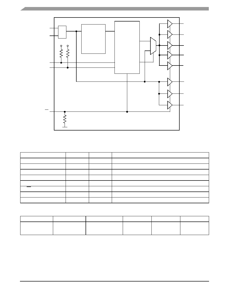
The MPC9817 uses a PLL with a 25-MHz input reference frequency to generate a single bank of five configurable LVCMOS
output clocks. The output frequency of this bank is configurable to either 25, 33, 50, or 66 MHz by two FSEL pins. The 25-MHz
reference may be either an external frequency source or a 25-MHz crystal. The 25-MHz crystal is directly connected to the
XTAL_IN and XTAL_OUT pins with no additional components required. An external reference may be applied to the XTAL_IN
pin with the XTAL_OUT pin left floating. The input reference, whether provided by a crystal or an external input, is also directly
buffered to a second bank of three LVCMOS outputs. These outputs may be used as the clock source for processor I/O
applications such as an Ethernet PHY. When FSEL0 and FSEL1 are both configured low, the QA outputs are directly fed from
the input reference providing a total of eight low-skew 25-MHz outputs. For all other combinations of FSEL0 and FSEL1 the
single-ended LVCMOS outputs provide five low-skew outputs for use in driving a microprocessor or microcontroller clock input
as well as other system components.
The MPC9817 is packaged in a 20-lead SSOP package.
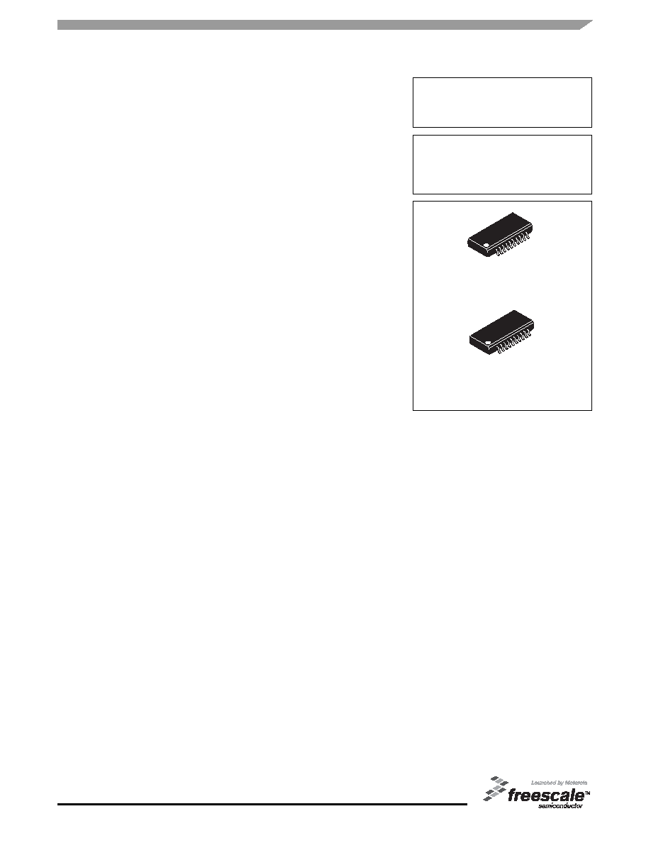
MPC9817
MICROPROCESSOR
CLOCK GENERATOR
EN SUFFIX
20 SSOP PACKAGE
Pb-FREE PACKAGE
CASE 1461-01
SD SUFFIX
20 SSOP PACKAGE
CASE 1461-01
Advanced Clock Drivers Devices
2
Freescale Semiconductor
MPC9817
Figure 1. MPC9817 Logic Diagram
Table 1. Pin Configurations
Pin
I/O
Type
Function
QA0, QA1, QA2, QA3, QA4
Output
LVCMOS
Clock Outputs
QREF0, QREF1, QREF2
Output
LVCMOS
Reference Output (25 MHz)
XTAL_IN
Input
LVCMOS
Crystal Oscillator Input Pin
XTAL_OUT
Output
LVCMOS
Crystal Oscillator Output Pin
FSEL0, FSEL1
Input
LVCMOS
Configures Bank A Clock Output Frequency (pull-up)
MR/OE
Input
LVCMOS
Enables All Outputs (pull-down)
V
DD
--
--
3.3-V Supply
GND
--
--
Ground
Table 2. Function Table
Control
Default
00
01
10
11
FSEL0,FSEL1
11
25 MHz fed directly
from reference input,
PLL disabled
33 MHz
50 MHz
66 MHz
Ref
PLL
400 MHz
QA0
QA1
QA2
QA4
XTAL_IN
OSC
XTAL_OUT
FSEL0
QREF0
FSEL1
QA3
QREF1
QREF2
Data
Generator
MR/OE
33,50,66 MHz
25 MHz
Advanced Clock Drivers Devices
Freescale Semiconductor
3
MPC9817
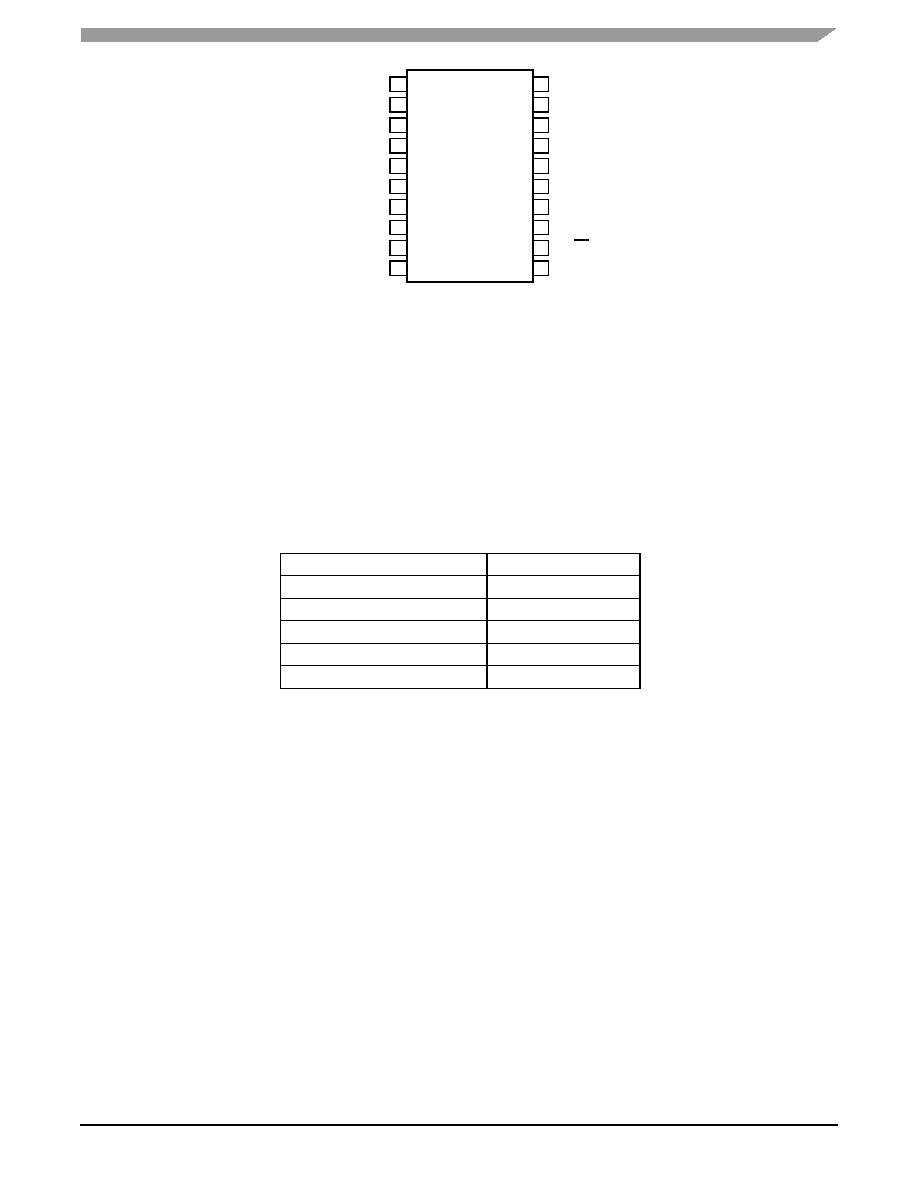
Figure 2. MPC9817 20-Lead SSOP Package Pinout (Top View)
MPC9817 OPERATION
Crystal Oscillator
The MPC9817 features a fully integrated Pierce oscillator
to minimize system implementation costs. Other than the
addition of a 25-MHz crystal, no external components are
required.The crystal selection should be: 25 MHz, parallel
resonant type with a load specification of C
L
= 10 pF. Crystals
with a load specification of C
L
= 20 pF may be used, however,
the reference frequency may be higher than the specified
25 MHz. Externally supplied capacitors on both the XTAL_IN
and XTAL_OUT pins may be used to trim the frequency as
desired.
The crystal should be located as close to the MPC9817
XTAL_IN and XTAL_OUT pins as possible to avoid any board
level parasitic.
Power Supply Bypassing
The MPC9817 should have all V
DD
pins bypassed with
0.01 capacitors and a minimum of one 1.0 capacitor for the
overall package. All capacitors should be located as close to
the SSOP pins as possible.
External Clock Source
An external reference source of 25 MHz may be applied to
the XTAL_IN pin. In this mode of operation, the XTAL_OUT
pin should be left floating.
XTAL_IN
XTAL_OUT
FSEL0
V
DD
FSEL1
QREF2
GND
QREF1
QREF0
V
DD
V
DD
QA4
QA3
GND
QA2
QA1
V
DD
QA0
MR/OE
GND
1
2
3
4
5
6
7
8
9
10
20
19
18
17
16
15
14
13
12
11
Table 3. Crystal Specifications
Parameter
Value
Crystal Cut
Fundamental AT Cut
Resonance
Parallel Resonance
Shunt Capacitance (C
L
)
5≠7 pF
Load Capacitance (C
O
)
10 pF
Equivalent Series Resistance (ESR)
20≠60
Advanced Clock Drivers Devices
4
Freescale Semiconductor
MPC9817
Table 4. Absolute Maximum Ratings
(1)
1. Absolute maximum continuous ratings are those maximum values beyond which damage to the device may occur. Exposure to these
conditions or conditions beyond those indicated may adversely affect device reliability. Functional operation at absolute-maximum-rated
conditions is not implied.
Symbol
Characteristics
Min
Max
Unit
Condition
V
DD
Supply Voltage
≠0.3
3.8
V
I
IN
DC Input Current
--
±20
mA
I
OUT
DC Output Current
--
±75
mA
T
S
Storage Temperature
≠65
125
∞C
Table 5. General Specifications
Symbol
Characteristics
Min
Typ
Max
Unit
Condition
V
TT
Output Termination Voltage
--
V
DD
˜ 2
--
V
MM
ESD Protection (machine model)
200
--
--
V
HBM
ESD Protection (human body model)
2000
--
--
V
LU
Latch-Up Immunity
200
--
--
mA
C
IN
Input Capacitance
--
4
--
pF
Inputs
JA
Thermal Resistance (junction-to-ambient)
--
80.8
--
∞C/W
T
C
Ambient Temperature
≠40
85
∞C
Table 6. DC Characteristics (V
DD
= 3.3 V ± 5%, T
A
= ≠40∞ to +85∞C)
Symbol
Characteristics
Min
Typ
Max
Unit
Condition
V
IH
Input High Voltage (XTAL_IN)
2.4
--
V
DD
+ 0.3
V
Input threshold = V
DD
/2
V
IH
Input High Voltage
2.0
--
V
DD
+ 0.3
V
V
IL
Input Low Voltage
--
--
0.8
V
LVCMOS
I
IN
Input Current
(1)
1. Inputs have pull-down resistors affecting the input current.
--
--
150
µ
A
V
IN
= V
DDL
or GND
V
OH
Output High Voltage
2.4
--
--
V
I
OH
= ≠12 mA
V
OL
Output Low Voltage
--
--
0.4
V
I
OL
= 12 mA
Z
OUT
Output Impedance
--
14
--
I
DD
Maximum Quiescent Supply Current
--
8.0
15.0
mA
V
DD
pins
Advanced Clock Drivers Devices
Freescale Semiconductor
5
MPC9817
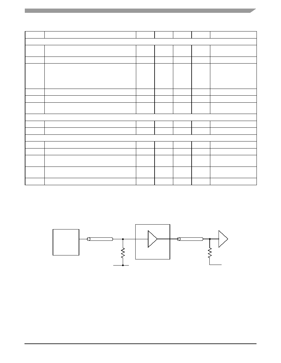
Figure 3. MPC9817 AC Test Reference (LVCMOS Outputs)
Table 7. AC Characteristics
(1)
(2)
(V
DD
= 3.3 V ± 5%, T
A
= ≠40∞ to +85∞C)
1. AC characteristics are design targets and pending characterization.
2. AC characteristics apply for parallel output termination of 50
to V
TT
.
Symbol
Characteristics
Min
Typ
Max
Unit
Condition
Input and Output Timing Specification
f
ref
Input Reference Frequency
25 MHz Input
XTAL Input
25
25
MHz
MHz
f
VCO
VCO Frequency Range
--
400
--
MHz
f
MCX
Output Frequency (QAx)
FSEL0, FSEL1 = 00
FSEL0, FSEL1 = 01
FSEL0, FSEL1 = 10
FSEL0, FSEL1 = 11
Output Frequency (QREFx)
25
33
50
66
25
--
--
--
--
--
MHz
MHz
MHz
MHz
MHz
PLL locked
f
refPW
Reference Input Pulse Width
10
--
--
ns
@ 25 MHz
DC
Output Duty Cycle
47.5
50
52.5
%
f
out
Output Frequency Accuracy
Crystal
(3)
External Reference
3. Based upon recommended crystal specifications as outlined in operation section.
--
--
100
0
ppm
ppm
With recommended crystal
see Table 3
PLL Specifications
BW
PLL Closed Loop Bandwidth
(4)
4. ≠3 dB point of PLL transfer characteristics.
500
kHz
t
LOCK
Maximum PLL Lock Time
10
ms
Skew and Jitter Specifications
t
sk(O)
Output-to-Output Skew (within a bank)
100
ps
t
sk(O)
Output-to-Output Skew (between bank A and bank Ref)
200
FSEL0, FSEL1 = 00
t
JIT(CC)
Cycle-to-Cycle Jitter
150
ps
@ 25 MHz Input Reference
Q
A
output
t
JIT(PER)
Period Jitter
100
ps
@ 25 MHz Input Reference
Q
A
output
t
r
, t
f
Output Rise/Fall Time
1
ns
20% to 80%
Z = 50
R
T
= 50
V
TT
Z = 50
V
TT
DUT MPC9817
Pulse
Generator
Z = 50
R
T
= 50
Advanced Clock Drivers Devices
6
Freescale Semiconductor
MPC9817
Table 8. MPC9817 Pin List
Pin
Description
Pin
Description
1
XTAL_IN
11
GND
2
XTAL_OUT
12
MR/OE
3
FSEL0
13
QA0
4
V
DD
14
V
DD
5
FSEL1
15
QA1
6
QREF2
16
QA2
7
GND
17
GND
8
QREF1
18
QA3
9
QREF0
19
QA4
10
V
DD
20
V
DD
Advanced Clock Drivers Devices
Freescale Semiconductor
7
MPC9817
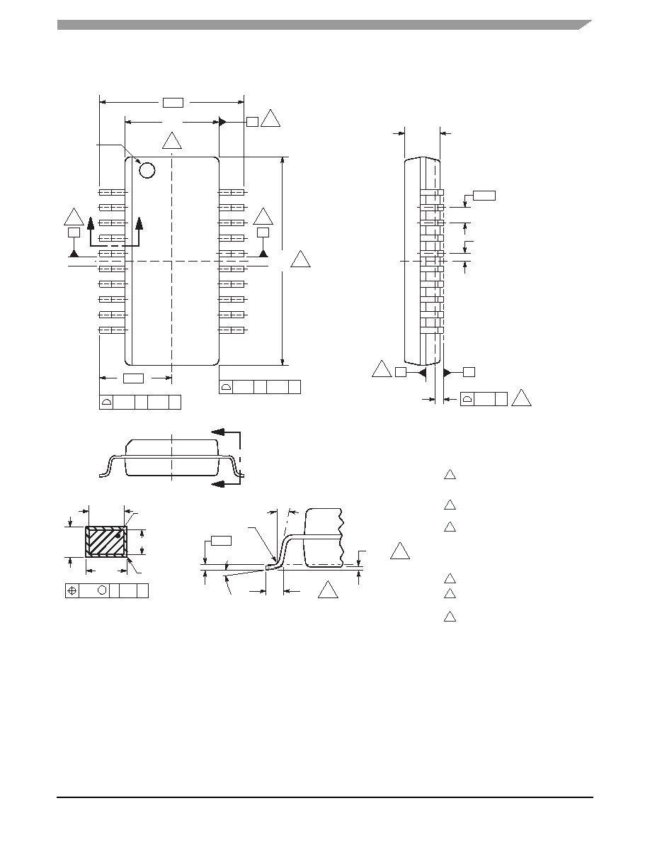
PACKAGE DIMENSIONS
.337
.150
1
10
11
20
B
PIN 1 ID
4
5
D
.157
.344
4
.236
.118
.010
C
A-B
D
2X 10 TIPS
B
B
5
.003
H
A-B
D
2X
A
4
.035
SECTION B-B
R.003 MIN
.0098
.0040
.016
0∞
8∞
0∞
.010
GAUGE PLANE
MIN
8
6
.004 C
.055
SEATING
PLANE
.025
C
20X
18X
.061
.0125
CL
H
3
7
A
A
(.010)
.012
.010
(.008)
PLATING
BASE METAL
SECTION A-A
.007
.008
M
.007
C A-B D
NOTES:
1.
2.
3.
4.
5.
6.
7.
8.
DIMENSIONS ARE IN INCHES.
DIMENSIONING AND TOLERANCING PER ASME
Y14.5M, 1994.
DATUM PLANE H LOCATED AT MOLD PARTING
LINE AND COINCIDENT WITH LEAD, WHERE
LEAD EXITS PLASTIC BODY AT BOTTOM OF
PARTING LINE.
DATUM A, B AND D TO BE DETRMINED WHERE
CENTERLINE BETWEEN LEADS EXITS PLASTIC
BODY AT DATUM PLANE H.
THIS DIMENSION DOES NOT INCLUDE MOLD
FLASH OR PROTRUSIONS, BUT DO INCLUDE
MOLD MISMATCH AND ARE MEASURED AT THE
MOLD PARTING LINE. MOLD FLASH OR
PROTRUSIONS SHALL NOT EXCEED .006
INCHES FOR ENDS AND .008 INCHES FOR
SIDES.
THIS DIMENSION IS LENGTH OF TERMINAL FOR
SOLDERING A SUBSTRATE.
FORMED LEADS SHALL BE PLANAR WITH
RESPECT TO ONE ANOTHER WITHIN .004
INCHES AT SEATING PLANE.
THIS DIMENSION IS DEFINED AS THE DISTANCE
FROM THE SEATING PLANE TO THE LOWEST
POINT OF THE PACKAGE BODY.
CASE 1461-02
ISSUE O
20 SSOP PACKAGE

How to Reach Us:
Home Page:
www.freescale.com
E-mail:
support@freescale.com
USA/Europe or Locations Not Listed:
Freescale Semiconductor
Technical Information Center, CH370
1300 N. Alma School Road
Chandler, Arizona 85224
+1-800-521-6274 or +1-480-768-2130
support@freescale.com
Europe, Middle East, and Africa:
Freescale Halbleiter Deutschland GmbH
Technical Information Center
Schatzbogen 7
81829 Muenchen, Germany
+44 1296 380 456 (English)
+46 8 52200080 (English)
+49 89 92103 559 (German)
+33 1 69 35 48 48 (French)
support@freescale.com
Japan:
Freescale Semiconductor Japan Ltd.
Headquarters
ARCO Tower 15F
1-8-1, Shimo-Meguro, Meguro-ku,
Tokyo 153-0064
Japan
0120 191014 or +81 3 5437 9125
support.japan@freescale.com
Asia/Pacific:
Freescale Semiconductor Hong Kong Ltd.
Technical Information Center
2 Dai King Street
Tai Po Industrial Estate
Tai Po, N.T., Hong Kong
+800 2666 8080
support.asia@freescale.com
For Literature Requests Only:
Freescale Semiconductor Literature Distribution Center
P.O. Box 5405
Denver, Colorado 80217
1-800-441-2447 or 303-675-2140
Fax: 303-675-2150
LDCForFreescaleSemiconductor@hibbertgroup.com
MPC9817
Rev. 1
11/2004
Information in this document is provided solely to enable system and software
implementers to use Freescale Semiconductor products. There are no express or
implied copyright licenses granted hereunder to design or fabricate any integrated
circuits or integrated circuits based on the information in this document.
Freescale Semiconductor reserves the right to make changes without further notice to
any products herein. Freescale Semiconductor makes no warranty, representation or
guarantee regarding the suitability of its products for any particular purpose, nor does
Freescale Semiconductor assume any liability arising out of the application or use of any
product or circuit, and specifically disclaims any and all liability, including without
limitation consequential or incidental damages. "Typical" parameters that may be
provided in Freescale Semiconductor data sheets and/or specifications can and do vary
in different applications and actual performance may vary over time. All operating
parameters, including "Typicals", must be validated for each customer application by
customer's technical experts. Freescale Semiconductor does not convey any license
under its patent rights nor the rights of others. Freescale Semiconductor products are
not designed, intended, or authorized for use as components in systems intended for
surgical implant into the body, or other applications intended to support or sustain life,
or for any other application in which the failure of the Freescale Semiconductor product
could create a situation where personal injury or death may occur. Should Buyer
purchase or use Freescale Semiconductor products for any such unintended or
unauthorized application, Buyer shall indemnify and hold Freescale Semiconductor and
its officers, employees, subsidiaries, affiliates, and distributors harmless against all
claims, costs, damages, and expenses, and reasonable attorney fees arising out of,
directly or indirectly, any claim of personal injury or death associated with such
unintended or unauthorized use, even if such claim alleges that Freescale
Semiconductor was negligent regarding the design or manufacture of the part.
FreescaleTM and the Freescale logo are trademarks of Freescale Semiconductor, Inc.
All other product or service names are the property of their respective owners.
© Freescale Semiconductor, Inc. 2004. All rights reserved.