MPXV5050VC6T1
Rev 1, 05/2005
Freescale Semiconductor
Technical Data
MPXV5050VC6T1
Sensors
Freescale Semiconductor
1
High Temperature Accuracy
Integrated Silicon Pressure Sensor
On-Chip Signal Conditioned,
Temperature Compensated and
Calibrated
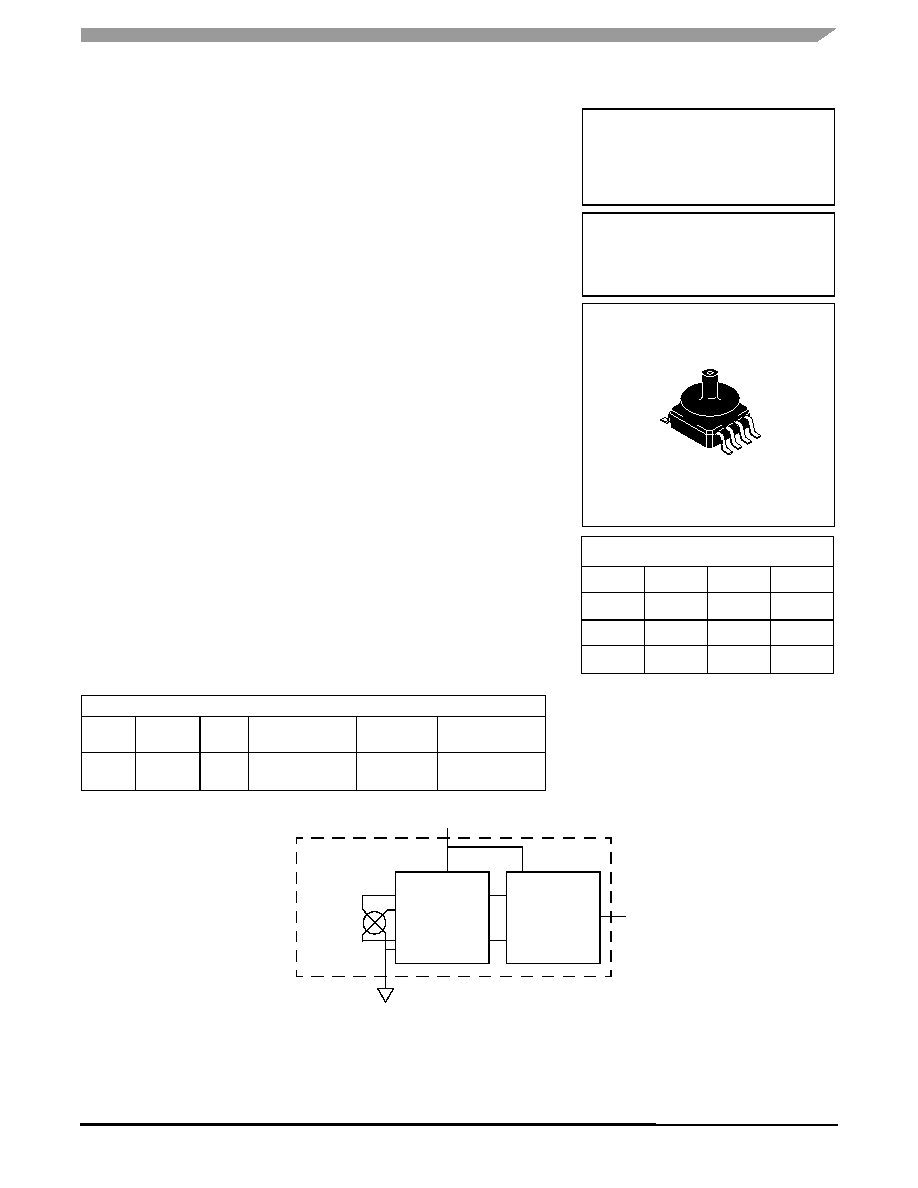
The MPXV5050VC6T1 sensor integrates on-chip, bipolar op amp circuitry and
thin film resistor networks to provide a high output signal and temperature
compensation. The small form factor and high reliability of on-chip integration
make the Freescale Semiconductor, Inc. pressure sensor a logical and
economical choice for the system designer.
The MPXV5050VC6T1 piezoresistive transducer is a state-of-the-art,
monolithic, signal conditioned, silicon pressure sensor. This sensor combines
advanced micromachining techniques, thin film metallization, and bipolar
semiconductor processing to provide an accurate, high level analog output signal
that is proportional to applied pressure.
Figure 1
shows a block diagram of the internal circuitry integrated on a
pressure sensor chip.
Features
∑
2.5% Maximum Error over 0
∞ to 85∞C
∑
Ideally suited for Microprocessor or Microcontroller-Based Systems
∑
Temperature Compensated from Over ≠40
∞ to +125∞C
∑
Patented Silicon Shear Stress Strain Gauge
∑
Durable Thermoplastic (PPS) Surface Mount Package
∑
Easy-to-Use Chip Carrier Option
∑
Ideal for Automotive and Non-Automotive Applications
Typical Applications
∑
Vacuum Pump Monitoring
Figure 1. Fully Integrated Pressure Sensor Schematic
ORDERING INFORMATION
Device
Type
Options
Case
No.
MPX Series
Order No.
Packing
Options
Device Marking
Ported
Element
Vacuum,
Axial Port
482A
MPXV5050VC6T1
Tape & Reel MPXV5050VC6T1
MPXV5050VC6T1
INTEGRATED
PRESSURE SENSOR
≠50 to 0 kPa (≠7.25 to 0 psi)
0.1 to 4.6 Volts Output
MPXV5050VC6T1
CASE 482A-01
SMALL OUTLINE PACKAGE
PIN NUMBER
(1)
1. Pins 1, 5, 6, 7, and 8 are internal device
connections. Do not connect to external
circuitry or ground. Pin 1 is noted by the
notch in the lead.
1
N/C
5
N/C
2
V
S
6
N/C
3
GND
7
N/C
4
V
OUT
8
N/C
Sensing
Element
Thin Film
Temperature
Compensation
and
Gain Stage #1
Gain Stage #2
and
Ground
Reference
Shift Circuitry
V
S
V
out
GND
Pins 1, 5, 6, 7, and 8 are NO CONNECTS
MPXV5050VC6T1
Sensors
2
Freescale Semiconductor
Table 1. Maximum Ratings
(1)
1. Exposure beyond the specified limits may cause permanent damage or degradation to the device.
Rating
Symbol
Value
Units
Maximum Pressure (P1 > P2)
P
max
200
kPa
Storage Temperature
T
stg
≠40∞ to +125∞
∞C
Operating Temperature
T
A
≠40∞ to +125∞
∞C
Table 2. Operating Characteristics
(
V
S
= 5.0 Vdc, T
A
= 25∞C unless otherwise noted, P1 > P2.)
Characteristic
Symbol
Min
Typ
Max
Unit
Pressure Range
P
OP
≠50
--
0
kPa
Supply Voltage
(1)
1. Device is ratiometric within this specified excitation range.
V
S
4.75
5.0
5.25
Vdc
Supply Current
I
o
--
7.0
10
mAdc
Full Scale Output
(2)
(0 to 85
∞C)
@ V
S
= 5.0 Volts
(P
diff
= 0 kPa)
2. Full Scale Output (V
FSO
) is defined as the output voltage at the maximum or full rated pressure.
V
FSO
4.488
4.6
4.713
Vdc
Full Scale Span
(3)
(0 to 85
∞C)
@ V
S
= 5.0 Volts
3. Full Scale Span (V
FSS
) is defined as the algebraic difference between the output voltage at full rated pressure and the output voltage at the
minimum rated pressure.
V
FSS
--
4.5
--
Vdc
Accuracy
(4)
(0 to 85
∞C)
4. Accuracy is the deviation in actual output from nominal output over the entire pressure range and temperature range as a percent of span
at 25∞C due to all sources of errors, including the following:
∑ Linearity:
Output deviation from a straight line relationship with pressure over the specified pressure range.
∑ Temperature Hysteresis: Output deviation at any temperature within the operating temperature range, after the temperature is cycled to
and from the minimum or maximum operating temperature points, with zero differential pressure applied.
∑ Pressure Hysteresis:
Output deviation at any pressure within the specified range, when this pressure is cycled to and from minimum
or maximum rated pressure at 25∞C.
∑ TcSpan:
Output deviation over the temperature range of 0∞ to 85∞C, relative to 25∞C.
∑ TcOffset:
Output deviation with minimum pressure applied, over the temperature range of 0∞ to 85∞C, relative to 25∞C.
--
--
--
±2.5
%V
FSS
Sensitivity
V/P
--
90
---
mV/kPa
Response Time
(5)
5. Response Time is defined as the time for the incremental change in the output to go from 10% to 90% of its final value when subjected to a
specified step change in pressure.
t
R
--
1.0
---
ms
Warm-Up Time
(6)
6. Warm-up Time is defined as the time required for the product to meet the specified output voltage after the pressure has been stabilized.
--
--
20
---
ms
Offset Stability
(7)
7. Offset Stability is the product's output deviation when subjected to 1000 hours of Pulsed Pressure, Temperature Cycling with Bias Test.
--
--
±0.5
---
%V
FSS
Pressure Offset
(8)
(0 to 85
∞C)
8. Offset (V
off
) is defined as the output voltage at the minimum rated pressure.
V
off
0
0.1
0.213
Vdc
MPXV5050VC6T1
Sensors
Freescale Semiconductor
3
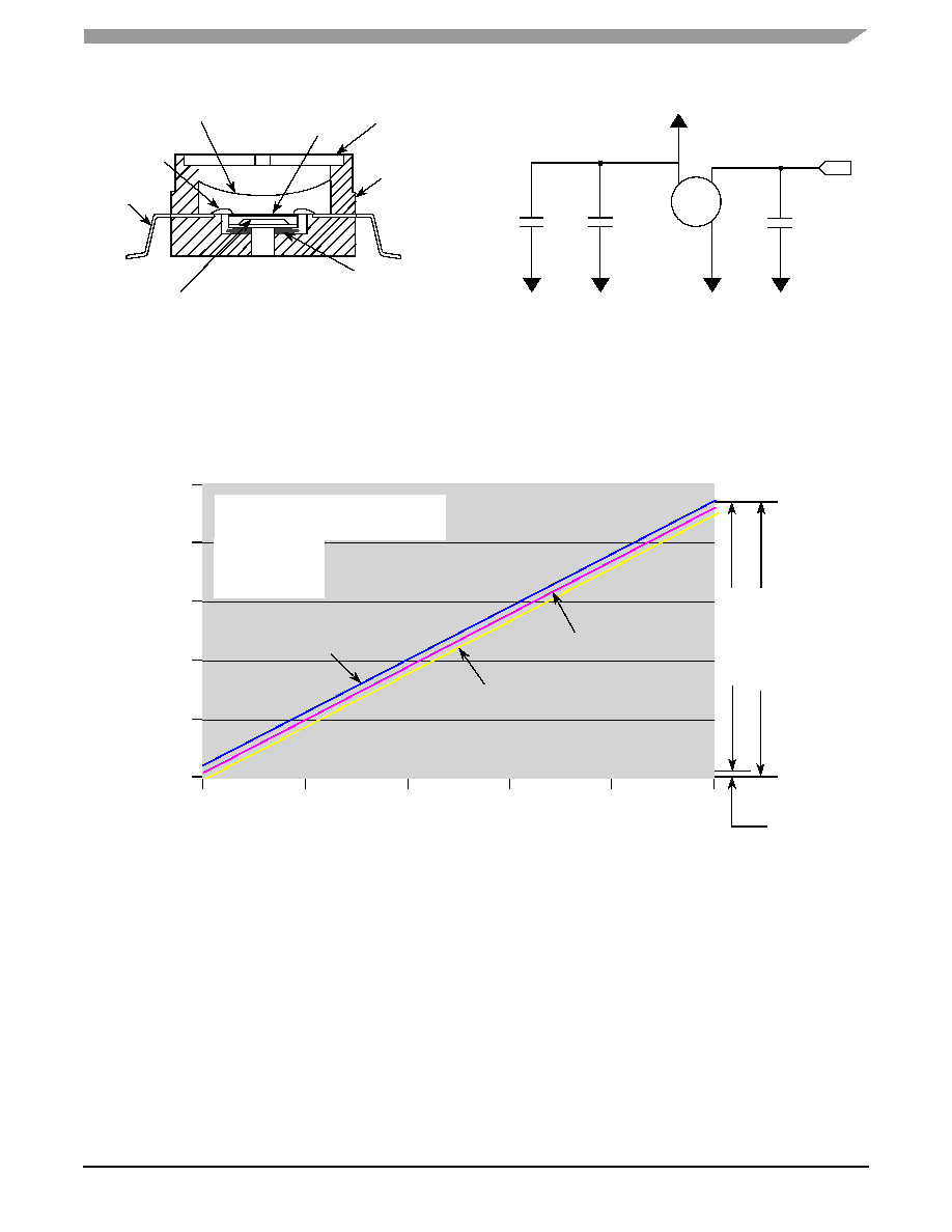
Figure 2. Cross-Sectional Diagram
(not to scale)
Figure 3. Typical Application Circuit
(Output Source Current Operation)
TRANSFER FUNCTION MPXV5050VC6T1
Figure 4. Output versus Absolute Pressure
Figure 4
shows the sensor output signal relative to
pressure input. Typical minimum and maximum output
curves are shown for operation over 0 to 85
∞C temperature
range. The output will saturate outside of the rated pressure
range.
A fluorosilicone gel isolates the die surface and wire bonds
from the environment, while allowing the pressure signal to
be transmitted to the silicon diaphragm. The
MPXV5050VC6T1 pressure sensor operating
characteristics, internal reliability and qualification tests are
based on use of dry air as the pressure media. Media other
than dry air may have adverse effects on sensor performance
and long-term reliability. Contact the factory for information
regarding media compatibility in your application.
DIFFERENTIAL SENSING ELEMENT
P2
WIRE BOND
STAINLESS
STEEL CAP
THERMOPLASTIC
CASE
DIE BOND
LEAD
FRAME
DIE
FLUOROSILICONE
GEL DIE COAT
P1
+5 V
1.0
µF
0.01
µF
470 pF
GND
V
s
V
out
IPS
OUTPUT
0
≠10
≠20
≠30
≠40
≠50
Pressure (kPa)
1
2
3
4
5
0
Outp
ut Volt
age (V)
Offset
(Typ)
Span
Ra
nge
(Typ)
Ou
tpu
t
Rang
e
(Ty
p
)
Transfer Function:
V
out
= V
S
x (0.018 x P + 0.92) ± (PE x TM x 0.018 x V
s
)
V
s
= 5.0 ± 0.25 vdc
PE = 1.25
TM = 1
Temperature = 0 to 85
∞C
MAX
MIN
TYPICAL
Transfer Function MPXV5050VC Series
MPXV5050VC6T1
Sensors
4
Freescale Semiconductor
Nominal Transfer Value:
V
out
= V
S
x (0.018 x P + 0.92)
± (Pressure Error x Temp Multi x 0.018 x V
S
)
V
S
= 5.0
± 0.25 V
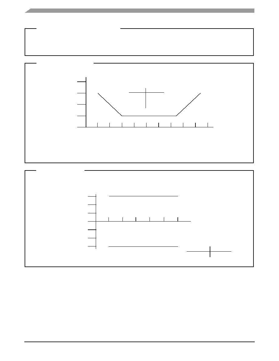
Transfer Function (MPXV5050VC6T1
Temp
Multiplier
≠40
3
0 to 85
1
+125
3
Temperature in ∞C
4.0
3.0
2.0
0.0
1.0
≠40
≠20
0
20
40
60
140
120
100
80
Temperature
Error
Factor
NOTE: The Temperature Multiplier is a linear response from 0∞C to ≠40∞C and from 85∞C to 125∞C.
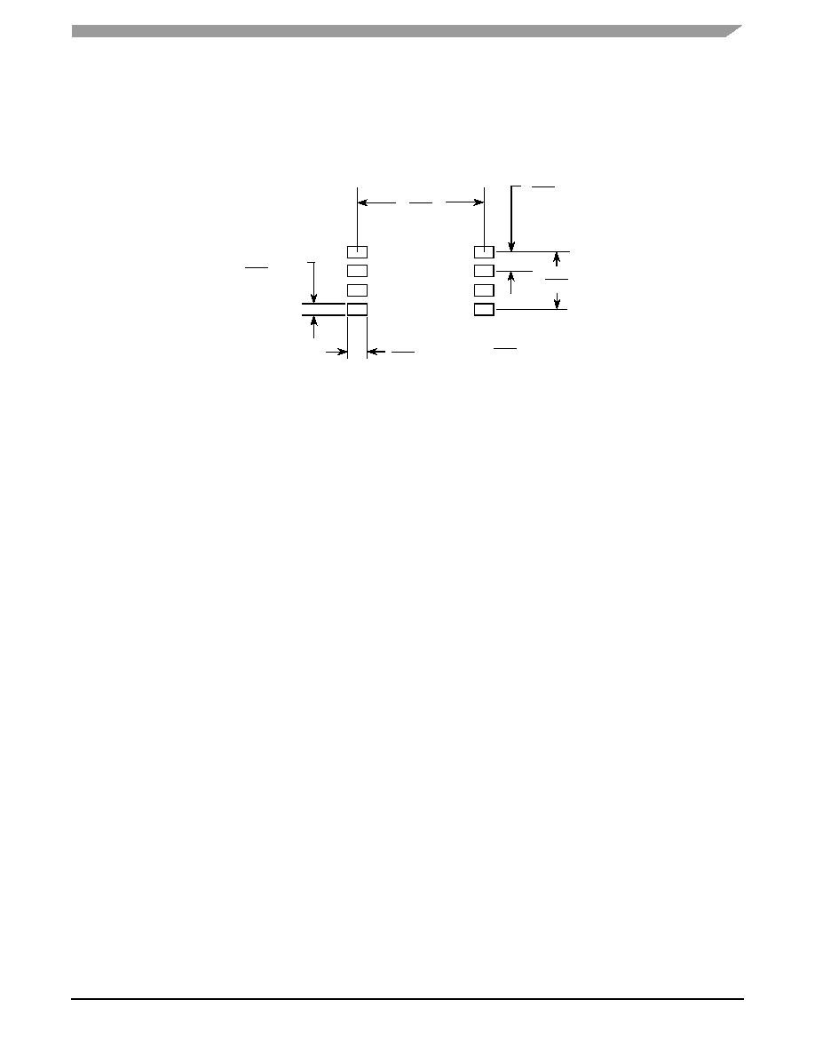
Temperature Error Band
Pressure
Error (Max)
Pressure Error Band
≠50 to 0 kPa
±1.25 kPa
MPXV5050V
≠50
0
Pressure (in kPa)
Pres
sur
e
Error
(k
Pa)
≠40
≠30
≠20
≠10
1.25
≠1.25
0
0.75
1.00
≠0.75
≠1.00
MPXV5050V
Error Limits for Pressure
MPXV5050V
Break Points
MPXV5050VC6T1
Sensors
Freescale Semiconductor
5
MINIMUM RECOMMENDED FOOTPRINT FOR SMALL OUTLINE PACKAGE
Surface mount board layout is a critical portion of the total
design. The footprint for the semiconductor package must be
the correct size to ensure proper solder connection interface
between the board and the package. With the correct pad
geometry, the packages will self-align when subjected to a
solder reflow process. It is always recommended to fabricate
boards with a solder mask layer to avoid bridging and/or
shorting between solder pads, especially on tight tolerances
and/or tight layouts.
Figure 5. SOP Footprint (Case 482A)
0.660
16.76
0.060 TYP 8X
1.52
0.100 TYP 8X
2.54
0.100 TYP
2.54
0.300
7.62
inch
mm
PACKAGE DIMENSIONS
PIN 1 IDENTIFIER
H
SEATING
PLANE
-T-
W
C
M
J
K
V
DIM
MIN
MAX
MIN
MAX
MILLIMETERS
INCHES
A
10.54
0.425
0.415
10.79
B
10.54
0.425
0.415
10.79
C
12.70
0.520
0.500
13.21
D
0.96
0.042
0.038
1.07
G
0.100 BSC
2.54 BSC
H
0.002
0.010
0.05
0.25
J
0.009
0.011
0.23
0.28
K
0.061
0.071
1.55
1.80
M
0∞
7∞
0∞
7∞
N
0.444
0.448
11.28
11.38
S
0.709
0.725
18.01
18.41
V
0.245
0.255
6.22
6.48
W
0.115
0.125
2.92
3.17
NOTES:
1. DIMENSIONING AND TOLERANCING PER ANSI
Y14.5M, 1982.
2. CONTROLLING DIMENSION: INCH.
3. DIMENSION A AND B DO NOT INCLUDE MOLD
PROTRUSION.
4. MAXIMUM MOLD PROTRUSION 0.15 (0.006).
5. ALL VERTICAL SURFACES 5∞ TYPICAL DRAFT.
S
D
8 PL
G
4
5
8
1
S
B
M
0.25 (0.010)
A
T
-A-
-B-
N
S
CASE 482A-01
ISSUE A
SMALL OUTLINE PACKAGE
MPXV5050VC6T1
Sensors
6
Freescale Semiconductor

MPXV5050VC6T1
Sensors
Freescale Semiconductor
7
NOTES

How to Reach Us:
Home Page:
www.freescale.com
E-mail:
support@freescale.com
USA/Europe or Locations Not Listed:
Freescale Semiconductor
Technical Information Center, CH370
1300 N. Alma School Road
Chandler, Arizona 85224
+1-800-521-6274 or +1-480-768-2130
support@freescale.com
Europe, Middle East, and Africa:
Freescale Halbleiter Deutschland GmbH
Technical Information Center
Schatzbogen 7
81829 Muenchen, Germany
+44 1296 380 456 (English)
+46 8 52200080 (English)
+49 89 92103 559 (German)
+33 1 69 35 48 48 (French)
support@freescale.com
Japan:
Freescale Semiconductor Japan Ltd.
Headquarters
ARCO Tower 15F
1-8-1, Shimo-Meguro, Meguro-ku,
Tokyo 153-0064
Japan
0120 191014 or +81 3 5437 9125
support.japan@freescale.com
Asia/Pacific:
Freescale Semiconductor Hong Kong Ltd.
Technical Information Center
2 Dai King Street
Tai Po Industrial Estate
Tai Po, N.T., Hong Kong
+800 2666 8080
support.asia@freescale.com
For Literature Requests Only:
Freescale Semiconductor Literature Distribution Center
P.O. Box 5405
Denver, Colorado 80217
1-800-441-2447 or 303-675-2140
Fax: 303-675-2150
LDCForFreescaleSemiconductor@hibbertgroup.com
Information in this document is provided solely to enable system and software
implementers to use Freescale Semiconductor products. There are no express or
implied copyright licenses granted hereunder to design or fabricate any integrated
circuits or integrated circuits based on the information in this document.
Freescale Semiconductor reserves the right to make changes without further notice to
any products herein. Freescale Semiconductor makes no warranty, representation or
guarantee regarding the suitability of its products for any particular purpose, nor does
Freescale Semiconductor assume any liability arising out of the application or use of any
product or circuit, and specifically disclaims any and all liability, including without
limitation consequential or incidental damages. "Typical" parameters that may be
provided in Freescale Semiconductor data sheets and/or specifications can and do vary
in different applications and actual performance may vary over time. All operating
parameters, including "Typicals", must be validated for each customer application by
customer's technical experts. Freescale Semiconductor does not convey any license
under its patent rights nor the rights of others. Freescale Semiconductor products are
not designed, intended, or authorized for use as components in systems intended for
surgical implant into the body, or other applications intended to support or sustain life,
or for any other application in which the failure of the Freescale Semiconductor product
could create a situation where personal injury or death may occur. Should Buyer
purchase or use Freescale Semiconductor products for any such unintended or
unauthorized application, Buyer shall indemnify and hold Freescale Semiconductor and
its officers, employees, subsidiaries, affiliates, and distributors harmless against all
claims, costs, damages, and expenses, and reasonable attorney fees arising out of,
directly or indirectly, any claim of personal injury or death associated with such
unintended or unauthorized use, even if such claim alleges that Freescale
Semiconductor was negligent regarding the design or manufacture of the part.
FreescaleTM and the Freescale logo are trademarks of Freescale Semiconductor, Inc.
All other product or service names are the property of their respective owners.
© Freescale Semiconductor, Inc. 2005. All rights reserved.
MPXV5050VC6T1
Rev. 1
05/2005