MRF1550NT1 MRF1550FNT1
1
RF Device Data
Freescale Semiconductor
RF Power Field Effect Transistors
N-Channel Enhancement-Mode Lateral MOSFETs
Designed for broadband commercial and industrial applications with frequen-
cies to 175 MHz. The high gain and broadband performance of these devices
make them ideal for large -signal, common source amplifier applications in
12.5 volt mobile FM equipment.
∑ Specified Performance @ 175 MHz, 12.5 Volts
Output Power -- 50 Watts
Power Gain -- 12 dB
Efficiency -- 50%
∑ Capable of Handling 20:1 VSWR, @ 15.6 Vdc, 175 MHz, 2 dB Overdrive
Features
∑ Excellent Thermal Stability
∑ Characterized with Series Equivalent Large-Signal Impedance Parameters
∑ Broadband -Full Power Across the Band: 135-175 MHz
∑ Broadband Demonstration Amplifier Information Available
Upon Request
∑ 200_C Capable Plastic Package
∑ N Suffix Indicates Lead-Free Terminations. RoHS Compliant.
∑ In Tape and Reel. T1 Suffix = 500 Units per 44 mm, 13 inch Reel.
Table 1. Maximum Ratings
Rating
Symbol
Value
Unit
Drain-Source Voltage
V
DSS
-0.5, +40
Vdc
Gate-Source Voltage
V
GS
±20
Vdc
Drain Current -- Continuous
I
D
12
Adc
Total Device Dissipation @ T
C
= 25∞C
(1)
Derate above 25∞C
P
D
165
0.50
W
W/∞C
Storage Temperature Range
T
stg
- 65 to +150
∞C
Operating Junction Temperature
T
J
200
∞C
Table 2. Thermal Characteristics
Characteristic
Symbol
Value
(2)
Unit
Thermal Resistance, Junction to Case
R
JC
0.75
∞C/W
Table 3. Moisture Sensitivity Level
Test Methodology
Rating
Package Peak Temperature
Unit
Per JESD 22-A113, IPC/JEDEC J-STD-020
1
260
∞C
1. Calculated based on the formula P
D
=
2. MTTF calculator available at http://www.freescale.com/rf. Select Tools/Software/Application Software/Calculators to access
the MTTF calculators by product.
NOTE - CAUTION - MOS devices are susceptible to damage from electrostatic charge. Reasonable precautions in handling and
packaging MOS devices should be observed.
Document Number: MRF1550N
Rev. 11, 9/2006
Freescale Semiconductor
Technical Data
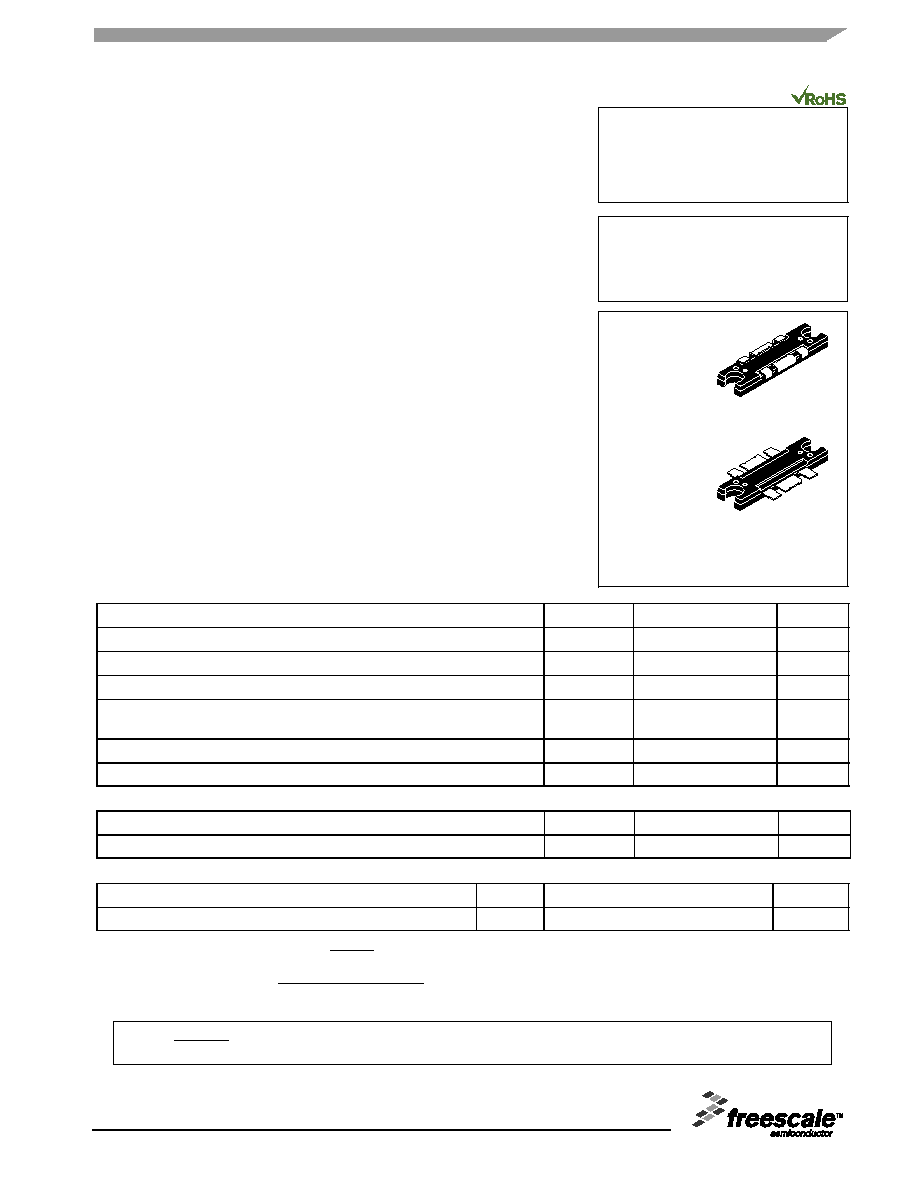
175 MHz, 50 W, 12.5 V
LATERAL N-CHANNEL
BROADBAND
RF POWER MOSFETs
MRF1550NT1
MRF1550FNT1
CASE 1264-09, STYLE 1
TO-272-6 WRAP
PLASTIC
MRF1550NT1
CASE 1264A-02, STYLE 1
TO-272-6
PLASTIC
MRF1550FNT1
TJ ≠ TC
RJC
© Freescale Semiconductor, Inc., 2006. All rights reserved.
2
RF Device Data
Freescale Semiconductor
MRF1550NT1 MRF1550FNT1
Table 4. Electrical Characteristics
(T
C
= 25∞C unless otherwise noted)
Characteristic
Symbol
Min
Typ
Max
Unit
Off Characteristics
Zero Gate Voltage Drain Current
(V
DS
= 60 Vdc, V
GS
= 0 Vdc)
I
DSS
--
--
1
Adc
Gate-Source Leakage Current
(V
GS
= 10 Vdc, V
DS
= 0 Vdc)
I
GSS
--
--
0.5
Adc
On Characteristics
Gate Threshold Voltage
(V
DS
= 12.5 Vdc, I
D
= 800 A)
V
GS(th)
1
--
3
Vdc
Drain-Source On-Voltage
(V
GS
= 5 Vdc, I
D
= 1.2 A)
R
DS(on)
--
--
0.5
Drain-Source On-Voltage
(V
GS
= 10 Vdc, I
D
= 4.0 Adc)
V
DS(on)
--
--
1
Vdc
Dynamic Characteristics
Input Capacitance (Includes Input Matching Capacitance)
(V
DS
= 12.5 Vdc, V
GS
= 0 V, f = 1 MHz)
C
iss
--
--
500
pF
Output Capacitance
(V
DS
= 12.5 Vdc, V
GS
= 0 V, f = 1 MHz)
C
oss
--
--
250
pF
Reverse Transfer Capacitance
(V
DS
= 12.5 Vdc, V
GS
= 0 V, f = 1 MHz)
C
rss
--
--
35
pF
RF Characteristics (In Freescale Test Fixture)
Common-Source Amplifier Power Gain
(V
DD
= 12.5 Vdc, P
out
= 50 Watts, I
DQ
= 500 mA)
f = 175 MHz
G
ps
--
14.5
--
dB
Drain Efficiency
(V
DD
= 12.5 Vdc, P
out
= 50 Watts, I
DQ
= 500 mA)
f = 175 MHz
--
55
--
%
MRF1550NT1 MRF1550FNT1
3
RF Device Data
Freescale Semiconductor
Figure 1. 135 - 175 MHz Broadband Test Circuit
B1
Ferroxcube #VK200
C1
180 pF, 100 mil Chip Capacitor
C2
10 pF, 100 mil Chip Capacitor
C3
33 pF, 100 mil Chip Capacitor
C4, C16
24 pF, 100 mil Chip Capacitors
C5
160 pF, 100 mil Chip Capacitor
C6
240 pF, 100 mil Chip Capacitor
C7, C17
300 pF, 100 mil Chip Capacitors
C8, C18
10 F, 50 V Electrolytic Capacitors
C9, C19
0.1 F, 100 mil Chip Capacitors
C10
470 pF, 100 mil Chip Capacitor
C11, C12
200 pF, 100 mil Chip Capacitors
C13
22 pF, 100 mil Chip Capacitor
C14
30 pF, 100 mil Chip Capacitor
C15
6.8 pF, 100 mil Chip Capacitor
C20
1,000 pF, 100 mil Chip Capacitor
L1
18.5 nH, Coilcraft #A05T
L2
5 nH, Coilcraft #A02T
L3
1 Turn, #24 AWG, 0.250 ID
L4
1 Turn, #26 AWG, 0.240 ID
L5
3 Turn, #24 AWG, 0.180 ID
N1, N2
Type N Flange Mounts
R1
5.1 , 1/4 W Chip Resistor
R2
39 Chip Resistor (0805)
R3
1 k, 1/8 W Chip Resistor
R4
33 k, 1/4 W Chip Resistor
Z1
1.000 x 0.080 Microstrip
Z2
0.400 x 0.080 Microstrip
Z3
0.200 x 0.080 Microstrip
Z4
0.200 x 0.080 Microstrip
Z5, Z6
0.100 x 0.223 Microstrip
Z7
0.160 x 0.080 Microstrip
Z8
0.260 x 0.080 Microstrip
Z9
0.280 x 0.080 Microstrip
Z10
0.270 x 0.080 Microstrip
Z11
0.730 x 0.080 Microstrip
Board
Glass Teflon
Æ
, 31 mils
V
DD
C8
R4
C9
C7
R3
RF
INPUT
RF
OUTPUT
Z2
Z3
Z6
C1
C3
C17
DUT
Z7
Z10
Z11
Z4
L5
Z8
N2
C21
N1
+
Z1
C2
V
GG
C18
+
C10
R2
C19
C20
L1
C5
C4
L2
Z5
C15
C13
C16
C14
C12
C11
Z9
C6
R1
L3
L4
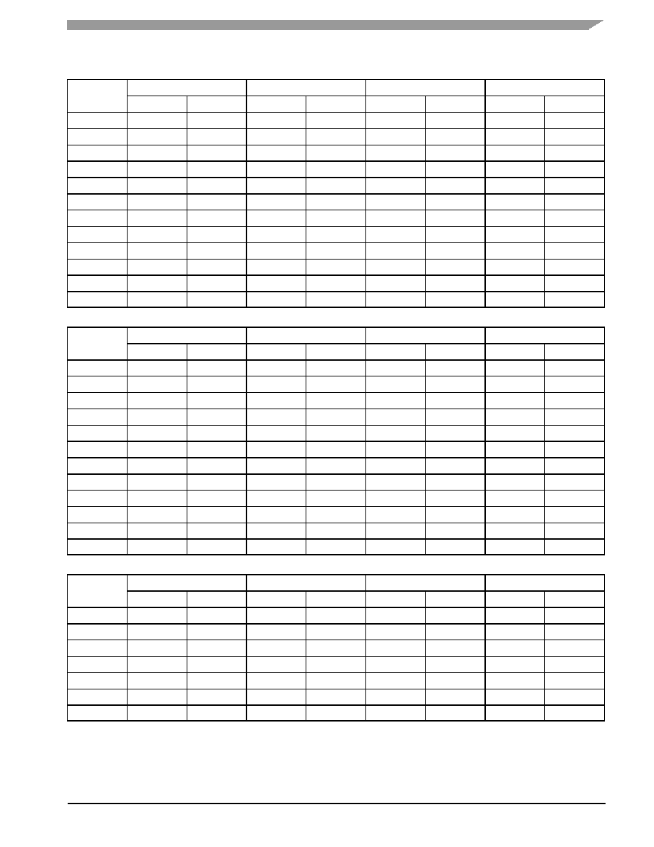
TYPICAL CHARACTERISTICS
P
out
, OUTPUT POWER (WATTS)
IRL,
INPUT
RETURN LOSS (dB)
-5
-15
-20
-10
20
0
10
Figure 2. Output Power versus Input Power
P
in
, INPUT POWER (WATTS)
10
Figure 3. Input Return Loss
versus Output Power
3.0
P out
,
OUTPUT
POWER (W
A
TTS)
0
30
5.0
1.0
20
175 MHz
155 MHz
4.0
6.0
2.0
0
60
135 MHz
30
155 MHz
175 MHz
135 MHz
50
40
50
40
60
70
80
V
DD
= 12.5 Vdc
V
DD
= 12.5 Vdc
70
80
4
RF Device Data
Freescale Semiconductor
MRF1550NT1 MRF1550FNT1
TYPICAL CHARACTERISTICS
50
20
P
out
, OUTPUT POWER (WATTS)
50
80
30
60
40
30
10
175 MHz
155 MHz
Figure 4. Gain versus Output Power
P
out
, OUTPUT POWER (WATTS)
11
10
14
Figure 5. Drain Efficiency versus Output Power
20
GAIN (dB)
Figure 6. Output Power versus Biasing Current
I
DQ
, BIASING CURRENT (mA)
Figure 7. Drain Efficiency versus
Biasing Current
70
I
DQ
, BIASING CURRENT (mA)
Figure 8. Output Power versus Supply Voltage
V
DD
, SUPPLY VOLTAGE (VOLTS)
Figure 9. Drain Efficiency versus Supply Voltage
V
DD
, SUPPLY VOLTAGE (VOLTS)
12
11
40
60
60
400
70
600
1000
80
55
65
12
16
200
50
13
P out
,
OUTPUT
POWER (W
A
TTS)
200
1000
400
600
P out
,
OUTPUT
POWER (W
A
TTS)
15
10
10
11
30
10
80
30
40
60
50
50
70
135 MHz
175 MHz
155 MHz
155 MHz
175 MHz
135 MHz
155 MHz
175 MHz
135 MHz
V
DD
= 12.5 Vdc
P
in
= 35 dBm
I
DQ
= 500 mA
P
in
= 35 dBm
V
DD
= 12.5 Vdc
P
in
= 35 dBm
V
DD
= 12.5 Vdc
40
60
70
50
80
15
40
60
70
50
80
70
V
DD
= 12.5 Vdc
800
60
70
800
40
14
12
13
80
90
15
13
14
175 MHz
155 MHz
135 MHz
135 MHz
1200
1200
I
DQ
= 500 mA
P
in
= 35 dBm
155 MHz
175 MHz
135 MHz
, DRAIN EFFICIENCY
(%)
h
, DRAIN EFFICIENCY
(%)
h
, DRAIN EFFICIENCY
(%)
h
MRF1550NT1 MRF1550FNT1
5
RF Device Data
Freescale Semiconductor
TYPICAL CHARACTERISTICS
210
10
11
T
J
, JUNCTION TEMPERATURE (
∞C)
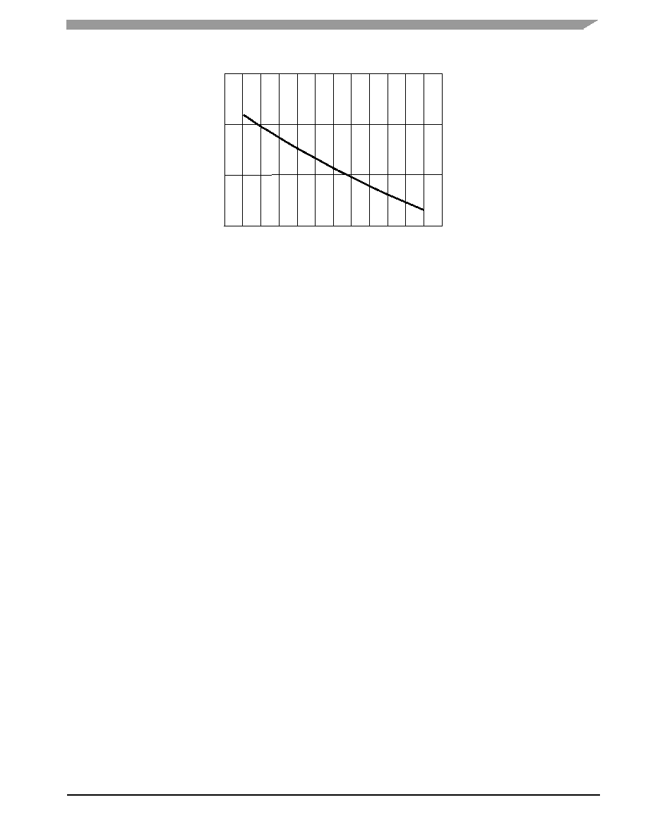
This above graph displays calculated MTTF in hours x ampere
2
drain current. Life tests at elevated temperatures have correlated to
better than
±10% of the theoretical prediction for metal failure. Divide
MTTF factor by I
D
2
for MTTF in a particular application.
10
10
10
8
MTTF
F
ACT
OR (HOURS X AMPS
2
)
90
110
130
150
170
190
100
120
140
160
180
200
Figure 10. MTTF Factor versus Junction Temperature
10
9
6
RF Device Data
Freescale Semiconductor
MRF1550NT1 MRF1550FNT1
Z
in
= Complex conjugate of source
impedance.
Z
OL
* = Complex conjugate of the load
impedance at given output power,
voltage, frequency, and
D
> 50 %.
f
MHz
Z
in
Z
OL
*
135
4.1 + j0.5
1.0 + j0.6
V
DD
= 12.5 V, I
DQ
= 500 mA, P
out
= 50 W
155
4.2 + j1.7
1.2 + j.09
175
3.7 + j2.3
0.7 + j1.1
f = 135 MHz
f = 175 MHz
Z
OL
*
Z
o
= 10
Z
in
f = 135 MHz
f = 175 MHz
Figure 11. Series Equivalent Input and Output Impedance
Zin
Z OL*
Input
Matching
Network
Device
Under Test
Output
Matching
Network
MRF1550NT1 MRF1550FNT1
7
RF Device Data
Freescale Semiconductor
Table 5. Common Source Scattering Parameters (V
DD
= 12.5 Vdc)
I
DQ
= 500 mA
f
S
11
S
21
S
12
S
22
f
MHz
|S
11
|
|S
21
|
|S
12
|
|S
22
|
50
0.93
-178
4.817
80
0.009
-39
0.86
-176
100
0.94
-178
2.212
69
0.009
-3
0.88
-175
150
0.95
-178
1.349
61
0.008
-8
0.90
-174
200
0.95
-178
0.892
54
0.006
-13
0.92
-174
250
0.96
-178
0.648
51
0.005
-7
0.93
-174
300
0.97
-178
0.481
47
0.004
-8
0.95
-174
350
0.97
-178
0.370
46
0.005
4
0.95
-174
400
0.98
-178
0.304
43
0.001
15
0.97
-174
450
0.98
-178
0.245
43
0.005
81
0.97
-174
500
0.98
-178
0.209
43
0.003
84
0.97
-174
550
0.99
-177
0.178
41
0.007
70
0.98
-175
600
0.98
-178
0.149
41
0.010
106
0.96
-175
I
DQ
= 2.0 mA
f
S
11
S
21
S
12
S
22
f
MHz
|S
11
|
|S
21
|
|S
12
|
|S
22
|
50
0.93
-177
4.81
80
0.003
-119
0.93
-178
100
0.94
-178
2.20
69
0.006
4
0.93
-178
150
0.95
-178
1.35
61
0.003
-1
0.93
-177
200
0.95
-178
0.89
54
0.004
18
0.93
-176
250
0.96
-178
0.65
51
0.001
28
0.94
-176
300
0.97
-178
0.48
47
0.004
77
0.94
-175
350
0.97
-178
0.37
46
0.006
85
0.95
-175
400
0.98
-178
0.30
43
0.007
53
0.96
-174
450
0.98
-178
0.25
43
0.006
74
0.97
-174
500
0.98
-177
0.21
44
0.006
84
0.97
-174
550
0.99
-177
0.18
41
0.002
106
0.97
-175
600
0.98
-178
0.15
41
0.004
116
0.96
-174
I
DQ
= 4.0 mA
f
S
11
S
21
S
12
S
22
f
MHz
|S
11
|
|S
21
|
|S
12
|
|S
22
|
50
0.97
-179
5.04
87
0.002
-116
0.94
-179
100
0.96
-179
2.43
82
0.006
42
0.94
-178
150
0.96
-179
1.60
77
0.004
13
0.94
-177
200
0.96
-179
1.14
74
0.003
43
0.95
-176
250
0.97
-179
0.89
71
0.004
65
0.95
-175
300
0.97
-179
0.71
68
0.006
68
0.95
-175
350
0.97
-179
0.57
67
0.006
74
0.97
-174

8
RF Device Data
Freescale Semiconductor
MRF1550NT1 MRF1550FNT1
Table 5. Common Source Scattering Parameters (V
DD
= 12.5 Vdc) (continued)
I
DQ
= 4.0 mA (continued)
f
S
11
S
21
S
12
S
22
f
MHz
|S
11
|
|S
21
|
|S
12
|
|S
22
|
400
0.97
-179
0.49
63
0.005
58
0.97
-173
450
0.98
-178
0.41
63
0.005
73
0.98
-173
500
0.98
-178
0.36
62
0.003
128
0.98
-173
550
0.98
-178
0.32
58
0.004
57
0.99
-174
600
0.98
-178
0.27
58
0.009
83
0.98
-174
MRF1550NT1 MRF1550FNT1
9
RF Device Data
Freescale Semiconductor
APPLICATIONS INFORMATION
DESIGN CONSIDERATIONS
This device is a common-source, RF power, N-Channel
enhancement mode, Lateral Metal -Oxide Semiconductor
Field -Effect Transistor (MOSFET). Freescale Application
Note AN211A, "FETs in Theory and Practice", is suggested
reading for those not familiar with the construction and char-
acteristics of FETs.
This surface mount packaged device was designed pri-
marily for VHF and UHF mobile power amplifier applications.
Manufacturability is improved by utilizing the tape and reel
capability for fully automated pick and placement of parts.
However, care should be taken in the design process to in-
sure proper heat sinking of the device.
The major advantages of Lateral RF power MOSFETs in-
clude high gain, simple bias systems, relative immunity from
thermal runaway, and the ability to withstand severely mis-
matched loads without suffering damage.
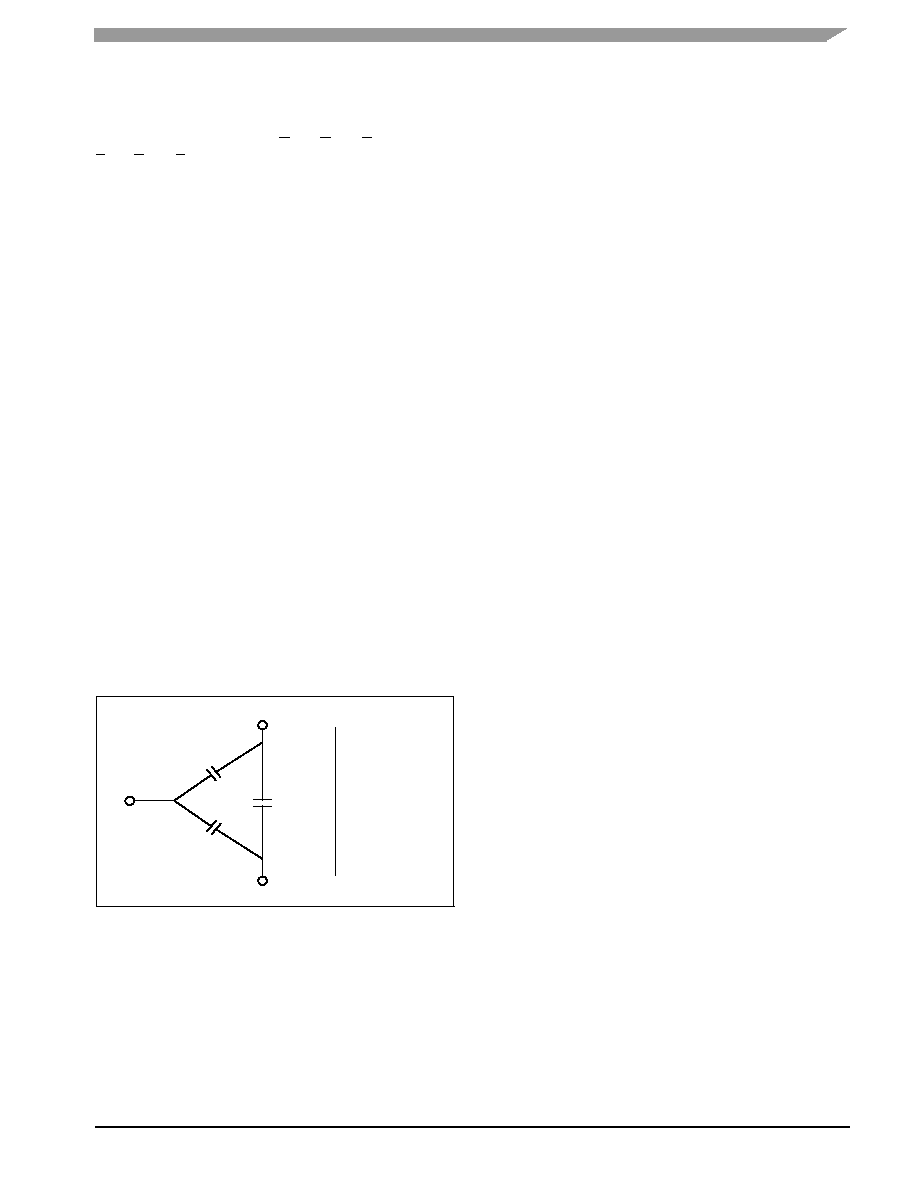
MOSFET CAPACITANCES
The physical structure of a MOSFET results in capacitors
between all three terminals. The metal oxide gate structure
determines the capacitors from gate -to -drain (C
gd
), and
gate-to-source (C
gs
). The PN junction formed during fab-
rication of the RF MOSFET results in a junction capacitance
from drain-to-source (C
ds
). These capacitances are charac-
terized as input (C
iss
), output (C
oss
) and reverse transfer
(C
rss
)
capacitances on data sheets. The relationships be-
tween the inter-terminal capacitances and those given on
data sheets are shown below. The C
iss
can be specified in
two ways:
1. Drain shorted to source and positive voltage at the gate.
2. Positive voltage of the drain in respect to source and zero
volts at the gate.
In the latter case, the numbers are lower. However, neither
method represents the actual operating conditions in RF ap-
plications.
Drain
C
ds
Source
Gate
C
gd
C
gs
C
iss
= C
gd
+ C
gs
C
oss
= C
gd
+ C
ds
C
rss
= C
gd
DRAIN CHARACTERISTICS
One critical figure of merit for a FET is its static resistance
in the full-on condition. This on-resistance, R
DS(on)
, occurs
in the linear region of the output characteristic and is speci-
fied at a specific gate-source voltage and drain current. The
drain - source voltage under these conditions is termed
V
DS(on)
. For MOSFETs, V
DS(on)
has a positive temperature
coefficient at high temperatures because it contributes to the
power dissipation within the device.
BV
DSS
values for this device are higher than normally re-
quired for typical applications. Measurement of BV
DSS
is not
recommended and may result in possible damage to the de-
vice.
GATE CHARACTERISTICS
The gate of the RF MOSFET is a polysilicon material, and
is electrically isolated from the source by a layer of oxide.
The DC input resistance is very high - on the order of 10
9
-- resulting in a leakage current of a few nanoamperes.
Gate control is achieved by applying a positive voltage to
the gate greater than the gate-to-source threshold voltage,
V
GS(th)
.
Gate Voltage Rating -- Never exceed the gate voltage
rating. Exceeding the rated V
GS
can result in permanent
damage to the oxide layer in the gate region.
Gate Termination -- The gates of these devices are es-
sentially capacitors. Circuits that leave the gate open-cir-
cuited or floating should be avoided. These conditions can
result in turn-on of the devices due to voltage build-up on
the input capacitor due to leakage currents or pickup.
Gate Protection -- These devices do not have an internal
monolithic zener diode from gate-to-source. If gate protec-
tion is required, an external zener diode is recommended.
Using a resistor to keep the gate-to-source impedance low
also helps dampen transients and serves another important
function. Voltage transients on the drain can be coupled to
the gate through the parasitic gate-drain capacitance. If the
gate-to-source impedance and the rate of voltage change
on the drain are both high, then the signal coupled to the gate
may be large enough to exceed the gate-threshold voltage
and turn the device on.
DC BIAS
Since this device is an enhancement mode FET, drain cur-
rent flows only when the gate is at a higher potential than the
source. RF power FETs operate optimally with a quiescent
drain current (I
DQ
), whose value is application dependent.
This device was characterized at I
DQ
= 150 mA, which is the
suggested value of bias current for typical applications. For
special applications such as linear amplification, I
DQ
may
have to be selected to optimize the critical parameters.
The gate is a dc open circuit and draws no current. There-
fore, the gate bias circuit may generally be just a simple re-
sistive divider network. Some special applications may
require a more elaborate bias system.
GAIN CONTROL
Power output of this device may be controlled to some de-
gree with a low power dc control signal applied to the gate,
thus facilitating applications such as manual gain control,
ALC/AGC and modulation systems. This characteristic is
very dependent on frequency and load line.

10
RF Device Data
Freescale Semiconductor
MRF1550NT1 MRF1550FNT1
AMPLIFIER DESIGN
Impedance matching networks similar to those used with
bipolar transistors are suitable for this device. For examples
see Freescale Application Note AN721, "Impedance
Matching Networks Applied to RF Power Transistors."
Large -signal impedances are provided, and will yield a good
first pass approximation.
Since RF power MOSFETs are triode devices, they are not
unilateral. This coupled with the very high gain of this device
yields a device capable of self oscillation. Stability may be
achieved by techniques such as drain loading, input shunt
resistive loading, or output to input feedback. The RF test fix-
ture implements a parallel resistor and capacitor in series
with the gate, and has a load line selected for a higher effi-
ciency, lower gain, and more stable operating region.
Two - port stability analysis with this device's
S-parameters provides a useful tool for selection of loading
or feedback circuitry to assure stable operation. See Free-
scale Application Note AN215A, "RF Small-Signal Design
Using Two-Port Parameters" for a discussion of two port
network theory and stability.
MRF1550NT1 MRF1550FNT1
11
RF Device Data
Freescale Semiconductor
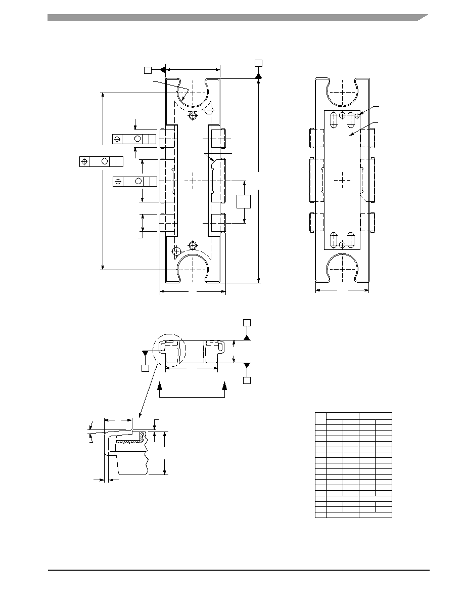
PACKAGE DIMENSIONS
TO-272-6 WRAP
PLASTIC
MRF1550NT1
««««
««««
««««
««««
««««
««««
««««
««««
««««
««««
««««
««««
««««
CASE 1264-09
ISSUE K
NOTES:
1. CONTROLLING DIMENSION: INCH .
2. INTERPRET DIMENSIONS AND TOLERANCES
PER ASME Y14.5M, 1994.
3. DATUM PLANE -H- IS LOCATED AT TOP OF LEAD
AND IS COINCIDENT WITH THE LEAD WHERE
THE LEAD EXITS THE PLASTIC BODY AT THE
TOP OF THE PARTING LINE.
4. DIMENSION D AND E1 DO NOT INCLUDE MOLD
PROTRUSION. ALLOWABLE PROTRUSION IS
0.006 PER SIDE. DIMENSION D AND E1 DO
INCLUDE MOLD MISMATCH AND ARE
DETERMINED AT DATUM PLANE -H-.
5. DIMENSIONS b1 AND b3 DO NOT INCLUDE
DAMBAR PROTRUSION. ALLOWABLE DAMBAR
PROTRUSION SHALL BE 0.005 TOTAL IN EXCESS
OF THE b1 AND b2 DIMENSIONS AT MAXIMUM
MATERIAL CONDITION.
6. CROSSHATCHING REPRESENTS THE EXPOSED
AREA OF THE HEAT SLUG.
L
A1
q
c1
H
D
C
A
B
M
aaa
D
SEATING
PLANE
DATUM
PLANE
SEATING
PLANE
2X
b1
A
E1
r1
DRAIN ID
e
4X
D
4X
b2
D1
A
M
aaa
D A
M
aaa
D A
E
DRAIN ID
Y
Y
A2
DIM
A
MIN
MAX
MIN
MAX
MILLIMETERS
0.098
0.108
2.49
2.74
INCHES
A1
0.000
0.004
0.00
0.10
A2
0.100
0.104
2.54
2.64
D
0.928
0.932
23.57
23.67
D1
0.806
0.814
20.47
20.68
E
0.296
0.304
7.52
7.72
E1
0.248
0.252
6.30
6.40
L
0.060
0.070
1.52
1.78
b1
0.193
0.199
4.90
5.05
b2
0.078
0.084
1.98
2.13
c1
0.007
0.011
0.18
0.28
e
r1
0.063
0.068
1.60
1.73
0 6 0
6
aaa
1
2
3
4
5
6
3
2
1
6
5
4
VIEW Y-Y
0.193 BSC
q
0.004
_
_
4.90 BSC
0.10
_
_
STYLE 1:
PIN 1. SOURCE (COMMON)
2. DRAIN
3. SOURCE (COMMON)
4. SOURCE (COMMON)
5. GATE
6. SOURCE (COMMON)
4X
b3
b3
0.088
0.094
2.24
2.39
NOTE 6
E2
E2
E2
0.241
0.245
6.12
6.22
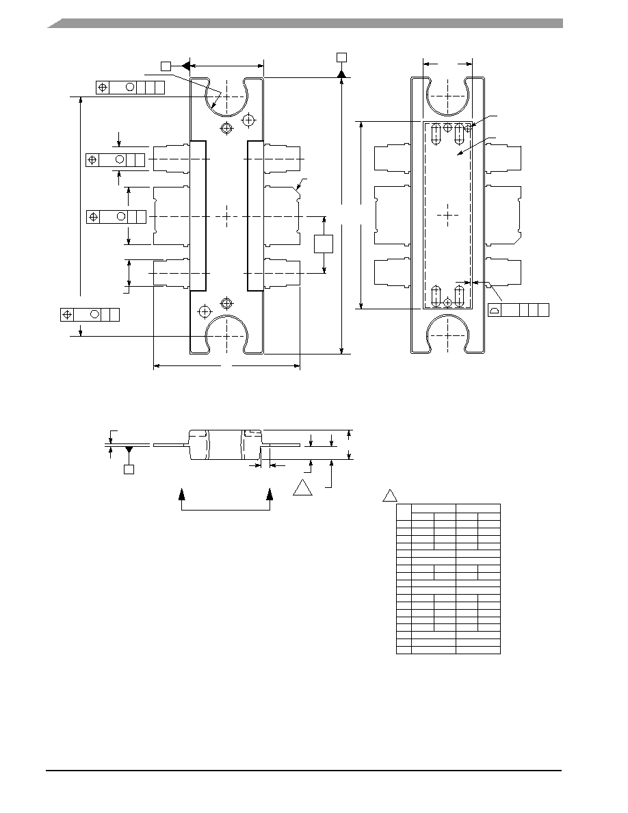
12
RF Device Data
Freescale Semiconductor
MRF1550NT1 MRF1550FNT1
««««
««««
««««
««««
««««
««««
««««
««««
««««
««««
««««
««««
««««
CASE 1264A-02
ISSUE C
NOTES:
1. CONTROLLING DIMENSION: INCH.
2. INTERPRET DIMENSIONS AND TOLERANCES
PER ASME Y14.5M, 1994.
3. DIMENSIONS D AND E1 DO NOT INCLUDE MOLD
PROTRUSION. ALLOWABLE PROTRUSION IS
0.006 PER SIDE. DIMENSIONS D AND E1 DO
INCLUDE MOLD MISMATCH AND ARE
DETERMINED AT DATUM PLANE -H-.
4. DIMENSIONS b1 AND b3 DO NOT INCLUDE
DAMBAR PROTRUSION. ALLOWABLE DAMBAR
PROTRUSION SHALL BE 0.005 TOTAL IN EXCESS
OF THE b1 AND b2 DIMENSIONS AT MAXIMUM
MATERIAL CONDITION.
5. CROSSHATCHING REPRESENTS THE EXPOSED
AREA OF THE HEAT SLUG.
6. DIMENSION A2 APPLIES WITHIN ZONE J ONLY.
D
A
B
M
aaa
D
SEATING
PLANE
2X
b1
A
E1
DRAIN ID
e
4X
D
4X
b2
D1
A
M
aaa
D A
M
aaa
D A
E
DRAIN ID
Y
Y
DIM
A
MIN
MAX
MIN
MAX
MILLIMETERS
0.098
0.106
2.49
2.69
INCHES
A1
0.038
0.044
0.96
1.12
D
0.926
0.934
23.52
23.72
D1
D2
E
0.492
0.500
12.50
12.70
E1
0.246
0.254
6.25
6.45
E2
P
0.126
0.134
3.20
3.40
b1
0.193
0.199
4.90
5.05
b3
0.088
0.094
2.24
2.39
e
c1
0.007
0.011
0.178
0.279
bbb
1
2
3
4
5
6
3
2
1
6
5
4
VIEW Y-Y
0.193 BSC
0.008
4.90 BSC
0.20
STYLE 1:
PIN 1. SOURCE (COMMON)
2. DRAIN
3. SOURCE (COMMON)
4. SOURCE (COMMON)
5. GATE
6. SOURCE (COMMON)
4X
b3
b2
0.078
0.084
1.98
2.13
NOTE 5
aaa
0.004
0.10
0.170 BSC
4.32 BSC
0.608 BSC
15.44 BSC
0.810 BSC
20.57 BSC
D2
E2
A
bbb
B
C
A1
c1
2X
P
M
aaa
D A B
ZONE "J"
F
F
0.025 BSC
0.64 BSC
A2
0.040
0.042
1.02
1.07
A2
6
TO-272-6
PLASTIC
MRF1550FNT1

MRF1550NT1 MRF1550FNT1
13
RF Device Data
Freescale Semiconductor
Information in this document is provided solely to enable system and software
implementers to use Freescale Semiconductor products. There are no express or
implied copyright licenses granted hereunder to design or fabricate any integrated
circuits or integrated circuits based on the information in this document.
Freescale Semiconductor reserves the right to make changes without further notice to
any products herein. Freescale Semiconductor makes no warranty, representation or
guarantee regarding the suitability of its products for any particular purpose, nor does
Freescale Semiconductor assume any liability arising out of the application or use of
any product or circuit, and specifically disclaims any and all liability, including without
limitation consequential or incidental damages. "Typical" parameters that may be
provided in Freescale Semiconductor data sheets and/or specifications can and do
vary in different applications and actual performance may vary over time. All operating
parameters, including "Typicals", must be validated for each customer application by
customer's technical experts. Freescale Semiconductor does not convey any license
under its patent rights nor the rights of others. Freescale Semiconductor products are
not designed, intended, or authorized for use as components in systems intended for
surgical implant into the body, or other applications intended to support or sustain life,
or for any other application in which the failure of the Freescale Semiconductor product
could create a situation where personal injury or death may occur. Should Buyer
purchase or use Freescale Semiconductor products for any such unintended or
unauthorized application, Buyer shall indemnify and hold Freescale Semiconductor
and its officers, employees, subsidiaries, affiliates, and distributors harmless against all
claims, costs, damages, and expenses, and reasonable attorney fees arising out of,
directly or indirectly, any claim of personal injury or death associated with such
unintended or unauthorized use, even if such claim alleges that Freescale
Semiconductor was negligent regarding the design or manufacture of the part.
Freescalet and the Freescale logo are trademarks of Freescale Semiconductor, Inc.
All other product or service names are the property of their respective owners.
© Freescale Semiconductor, Inc. 2006. All rights reserved.
How to Reach Us:
Home Page:
www.freescale.com
E-mail:
support@freescale.com
USA/Europe or Locations Not Listed:
Freescale Semiconductor
Technical Information Center, CH370
1300 N. Alma School Road
Chandler, Arizona 85224
+1-800-521-6274 or +1-480-768-2130
support@freescale.com
Europe, Middle East, and Africa:
Freescale Halbleiter Deutschland GmbH
Technical Information Center
Schatzbogen 7
81829 Muenchen, Germany
+44 1296 380 456 (English)
+46 8 52200080 (English)
+49 89 92103 559 (German)
+33 1 69 35 48 48 (French)
support@freescale.com
Japan:
Freescale Semiconductor Japan Ltd.
Headquarters
ARCO Tower 15F
1-8-1, Shimo-Meguro, Meguro-ku,
Tokyo 153-0064
Japan
0120 191014 or +81 3 5437 9125
support.japan@freescale.com
Asia/Pacific:
Freescale Semiconductor Hong Kong Ltd.
Technical Information Center
2 Dai King Street
Tai Po Industrial Estate
Tai Po, N.T., Hong Kong
+800 2666 8080
support.asia@freescale.com
For Literature Requests Only:
Freescale Semiconductor Literature Distribution Center
P.O. Box 5405
Denver, Colorado 80217
1-800-441-2447 or 303-675-2140
Fax: 303-675-2150
LDCForFreescaleSemiconductor@hibbertgroup.com
Document Number: MRF1550N
Rev. 11, 9/2006
RoHS-compliant and/or Pb-free versions of Freescale products have the functionality and electrical
characteristics of their non-RoHS-compliant and/or non-Pb-free counterparts. For further
information, see http://www.freescale.com or contact your Freescale sales representative.
For information on Freescale's Environmental Products program, go to http://www.freescale.com/epp.