 | –≠–ª–µ–∫—Ç—Ä–æ–Ω–Ω—ã–π –∫–æ–º–ø–æ–Ω–µ–Ω—Ç: MRF377HR5 | –°–∫–∞—á–∞—Ç—å:  PDF PDF  ZIP ZIP |
MRF377HR3 MRF377HR5
1
RF Device Data
Freescale Semiconductor
RF Power Field-Effect Transistors
N-Channel Enhancement-Mode Lateral MOSFETs
Designed for broadband commercial and industrial applications with frequen-
cies from 470 to 860 MHz. The high gain and broadband performance of these
devices make them ideal for large-signal, common source amplifier applications
in 32 volt digital television transmitter equipment.
∑ Typical Broadband DVBT OFDM Performance @ 470-860 MHz, 32 Volts,
I
DQ
= 2.0 A, 8K Mode, 64 QAM
Output Power -- 45 Watts Avg.
Power Gain 16.7 dB
Efficiency 21%
ACPR -58 dBc
∑ Typical Broadband ATSC 8VSB Performance @ 470-860 MHz, 32 Volts,
I
DQ
= 2.0 A
Output Power -- 80 Watts Avg.
Power Gain 16.5 dB
Efficiency 27.5%
IMD -31.3 dBc
∑ Capable of Handling 10:1 VSWR, @ 32 Vdc, 860 MHz, 45 Watts DVBT
OFDM Output Power
∑ Characterized with Series Equivalent Large-Signal Impedance Parameters
∑ Internally Input and Output Matched for Ease of Use
∑ Integrated ESD Protection
∑ Excellent Thermal Stability
∑ Lower Thermal Resistance Package
∑ Low Gold Plating Thickness on Leads, 40
µ
Nominal.
∑ In Tape and Reel. R3 Suffix = 250 Units per 56 mm, 13 inch Reel.
R5 Suffix = 50 Units per 56 mm, 13 inch Reel.
Table 1. Maximum Ratings
(1)
Rating
Symbol
Value
Unit
Drain-Source Voltage
V
DSS
- 0.5, +65
Vdc
Gate-Source Voltage
V
GS
- 0.5, +15
Vdc
Drain Current - Continuous
I
D
17
Adc
Total Device Dissipation @ T
C
= 25∞C
Derate above 25∞C
P
D
648
3.7
W
W/∞C
Storage Temperature Range
T
stg
- 65 to +150
∞C
Operating Junction Temperature
T
J
200
∞C
Table 2. Thermal Characteristics
Characteristic
Symbol
Value
(2,3)
Unit
Thermal Resistance, Junction to Case
Case Temperature 81∞C, 105 W CW
Case Temperature 77∞C, 45 W CW
R
JC
0.27
0.29
∞C/W
1. Each side of device measured separately.
2. MTTF calculator available at http://www.freescale.com/rf. Select Tools/Software/Application Software/Calculators to access
the MTTF calculators by product.
3. Refer to AN1955/D, Thermal Measurement Methodology of RF Power Amplifiers. Go to http://www.freescale.com/rf.
Select Documentation/Application Notes - AN1955.
NOTE - CAUTION - MOS devices are susceptible to damage from electrostatic charge. Reasonable precautions in handling and
packaging MOS devices should be observed.
MRF377H
Rev. 0, 1/2005
Freescale Semiconductor
Technical Data
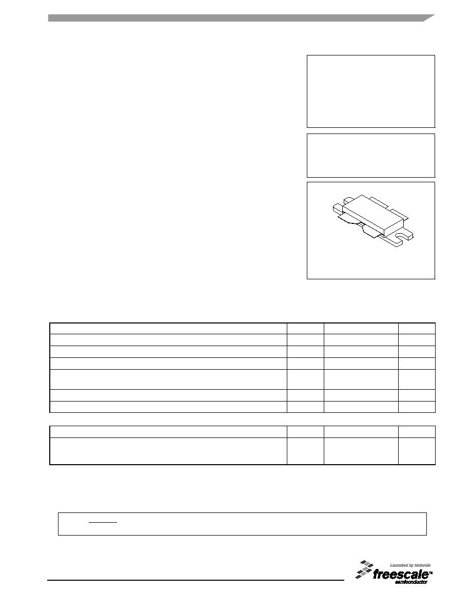
470 - 860 MHz, 240 W, 32 V
LATERAL N-CHANNEL
RF POWER MOSFETs
CASE 375G-04, STYLE 1
NI-860C3
MRF377HR3
MRF377HR5
Freescale Semiconductor, Inc., 2005. All rights reserved.

2
RF Device Data
Freescale Semiconductor
MRF377HR3 MRF377HR5
Table 3. ESD Protection Characteristics
Test Conditions
Class
Human Body Model
1 (Minimum)
Machine Model
M3 (Minimum)
Charge Device Model
7 (Minimum)
Table 4. Electrical Characteristics
(T
C
= 25∞C unless otherwise noted)
Characteristic
Symbol
Min
Typ
Max
Unit
Off Characteristics
(1)
Drain-Source Breakdown Voltage
(V
GS
= 0 Vdc, I
D
=10 µA)
V
(BR)DSS
65
--
--
Vdc
Zero Gate Voltage Drain Current
(V
DS
= 32 Vdc, V
GS
= 0 Vdc)
I
DSS
--
--
1
µAdc
Gate-Source Leakage Current
(V
GS
= 5 Vdc, V
DS
= 0 Vdc)
I
GSS
--
--
1
µAdc
Gate Threshold Voltage
(V
DS
= 10 Vdc, I
D
= 200 µA)
V
GS(th)
--
2.8
--
Vdc
On Characteristics
(1)
Gate Quiescent Voltage
(V
DS
= 32 Vdc, I
D
= 225 mA)
V
GS(Q)
--
3.5
--
Vdc
Drain-Source On-Voltage
(V
GS
= 10 Vdc, I
D
= 3 A)
V
DS(on)
--
0.27
--
Vdc
Dynamic Characteristics
(1)
Reverse Transfer Capacitance
(V
DS
= 28 Vdc, V
GS
= 0, f = 1 MHz)
C
rss
--
3.2
--
pF
Functional Characteristics (In DVBT OFDM Single-Channel, Narrowband Fixture,
50 ohm system)
(2)
Common Source Power Gain
(V
DD
= 32 Vdc, P
out
= 45 W Avg., I
DQ
= 2 x 1000 mA,
f = 860 MHz)
G
ps
16.5
18.2
--
dB
Drain Efficiency
(V
DD
= 32 Vdc, P
out
= 45 W Avg., I
DQ
= 2 x 1000 mA,
f = 860 MHz)
21
22.9
--
%
Adjacent Channel Power Ratio
(V
DD
= 32 Vdc, P
out
= 45 W Avg., I
DQ
= 2 x 1000 mA,
f = 860 MHz)
ACPR
--
-59.2
-57
dBc
Typical Characteristics (In DVBT OFDM Single-Channel, Broadband Fixture,
50 ohm system)
(2)
Common Source Power Gain
(V
DD
= 32 Vdc, P
out
= 45 W Avg., I
DQ
= 2 x 1000 mA)
f = 470 MHz
f = 560 MHz
f = 660 MHz
f = 760 MHz
f = 860 MHz
G
ps
--
--
--
--
--
17.6
17.6
17.4
17.4
16.8
--
--
--
--
--
dB
1. Each side of device measured separately.
2. Measured in push-pull configuration.
(continued)

MRF377HR3 MRF377HR5
3
RF Device Data
Freescale Semiconductor
Table 4. Electrical Characteristics
(T
C
= 25∞C unless otherwise noted)
(continued)
Characteristic
Symbol
Min
Typ
Max
Unit
Drain Efficiency
(V
DD
= 32 Vdc, P
out
= 45 W Avg., I
DQ
= 2 x 1000 mA)
f = 470 MHz
f = 560 MHz
f = 660 MHz
f = 760 MHz
f = 860 MHz
--
--
--
--
--
23.5
25.8
23.0
22.7
21.3
--
--
--
--
--
%
Adjacent Channel Power Ratio
(V
DD
= 32 Vdc, P
out
= 45 W Avg., I
DQ
= 2 x 1000 mA)
f = 470 MHz
f = 560 MHz
f = 660 MHz
f = 760 MHz
f = 860 MHz
ACPR
--
--
--
--
--
-59.3
-59.3
-58.7
-58.7
-58.1
--
--
--
--
--
dBc
Typical Characteristics (In ATSC 8VSB Single-Channel, Broadband Fixture,
50 ohm system)
(1)
Common Source Power Gain
(V
DD
= 32 Vdc, P
out
= 80 W Avg., I
DQ
= 2 x 1000 mA)
f = 470 MHz
f = 560 MHz
f = 660 MHz
f = 760 MHz
f = 860 MHz
G
ps
--
--
--
--
--
17.5
17.5
17.2
17.2
16.6
--
--
--
--
--
dB
Drain Efficiency
(V
DD
= 32 Vdc, P
out
= 80 W Avg., I
DQ
= 2 x 1000 mA)
f = 470 MHz
f = 560 MHz
f = 660 MHz
f = 760 MHz
f = 860 MHz
--
--
--
--
--
31.0
34.3
30.1
29.6
27.8
--
--
--
--
--
%
Intermodulation Distortion
(V
DD
= 32 Vdc, P
out
= 80 W Avg., I
DQ
= 2 x 1000 mA)
f = 470 MHz
f = 560 MHz
f = 660 MHz
f = 760 MHz
f = 860 MHz
IMD
--
--
--
--
--
31.7
32.7
32.9
34.2
35.4
--
--
--
--
--
dBc
1. Measured in push-pull configuration.

4
RF Device Data
Freescale Semiconductor
MRF377HR3 MRF377HR5
Table 5. 845-875 MHz Narrowband Test Circuit Component Designations and Values
Part
Description
Part Number
Manufacturer
B1, B2
Ferrite Beads, Surface Mount, 11 (0805)
2508051107Y0
Fair-Rite
Balun 1, Balun 2
0.8-1GHz Xinger Balun
3A412
Anaran
C1
33 pF Chip Capacitor (0805)
08055J330JBT
AVX / Kyocera
C2
2.7 pF Chip Capacitor (0603)
06035J2R7BBT
AVX / Kyocera
C3
12 pF Chip Capacitor (0805)
08051J120GBT
AVX / Kyocera
C4, C5
6.8 pF Chip Capacitors (0805)
08051J6R8BBT
AVX / Kyocera
C6
2.7 pF Chip Capacitor (0805)
0805J2R7BBT
AVX / Kyocera
C7, C8, C9, C10
3.3 pF Chip Capacitors (0805)
08051J3R3BBT
AVX / Kyocera
C11, C12
2.2 µF, 50 V Chip Capacitors
C1825C225J5RAC3810
Kemet
C13, C14, C15, C16
0.01 µF, 100 V Chip Capacitors
C1825C103J1GAC
Kemet
C17, C18
0.56 µF, 50 V Chip Capacitors
C1825C564J5RAC
Kemet
C19, C20
10 µF, 50 V Tantalum Chip Capacitors
522Z050/100MTRE
Tecate
C21, C22, C23, C24
47 µF, 16 V Tantalum Chip Capacitors
TPSD476K016R0150
AVX / Kyocera
C25, C26
470 µF, 63 V Electrolytic Capacitors
NACZF471M63V (18x22)
Nippon
L1
12 nH Inductor (0603)
0603HC-12NXJB
CoilCraft
L2
7.15 nH Inductor
1606-7
CoilCraft
L3, L4
10 nH Inductor (0603)
0603HC-10NXJB
CoilCraft
R1, R2
24 , 1/8 W, 5% Chip Resistors (1206)
WB1, WB2, WB3, WB4
Brass Wear Shims
PCB
Arlon 30 mil,
r
= 2.56
DS1152
DS Electronics
C10
C9
R1
C2
L1
C21
C22
C14
Balun 1
C3
WB2
WB1
L3
V
GG
B1
B2
C11
C1
R2
L4
V
GG
C24
C23
C12
C13
C15
C26
C18
Balun 2
C4
C5
C6
WB4
WB3
C25
V
DD
C16
C20
C17
L2
C8
C7
Figure 1. 845-875 MHz Narrowband Test Circuit Component Layout
MRF377 Gate
MRF377 Drain
C19
V
DD
DS1152-A Rev 0
DS1152-B Rev 0
Freescale has begun the transition of marking Printed Circuit Boards (PCBs) with the Freescale Semiconductor
signature/logo. PCBs may have either Motorola or Freescale markings during the transition period. These changes will have
no impact on form, fit or function of the current product.
MRF377HR3 MRF377HR5
5
RF Device Data
Freescale Semiconductor
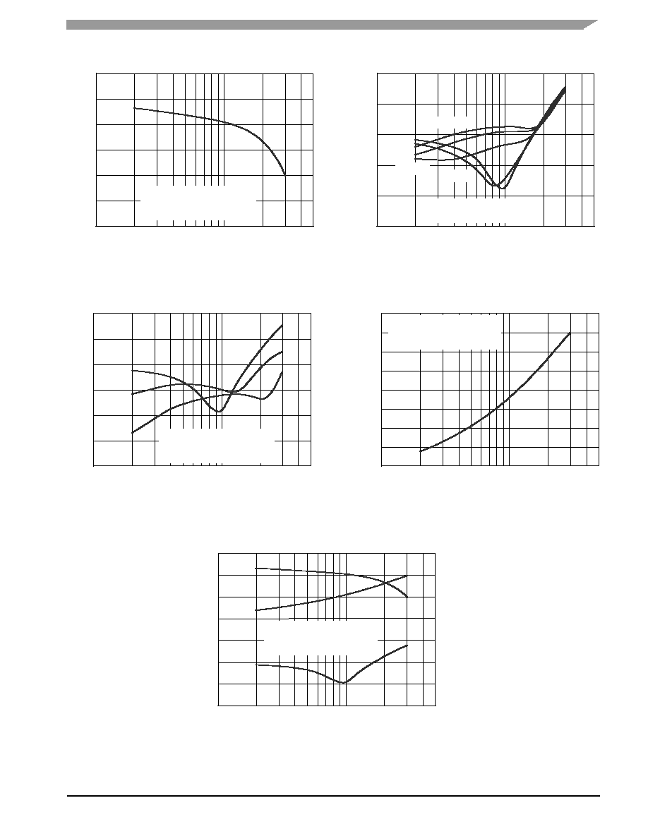
TYPICAL NARROWBAND CHARACTERISTICS
2200 mA
100
16
19
10
G
ps
P
out
, OUTPUT POWER (WATTS) PEP
Figure 2. Two-Tone Power Gain versus
Output Power
G
ps
, POWER GAIN (dB)
V
DD
= 32 Vdc
I
DQ
= 2000 mA
f1 = 859.95 MHz, f2 = 860.05 MHz
18.5
18
17.5
17
16.5
100
-70
-20
10
I
DQ
= 1400 mA
P
out
, OUTPUT POWER (WATTS) PEP
Figure 3. Third Order Intermodulation Distortion
versus Output Power
INTERMODULA
TION DIST
ORTION
(dBc)
IMD,
V
DD
= 32 Vdc
f1 = 859.95 MHz, f2 = 860.05 MHz
-30
-40
-50
-60
1600 mA
1800 mA
2000 mA
100
-80
-20
10
7th Order
P
out
, OUTPUT POWER (WATTS) PEP
Figure 4. Intermodulation Distortion Products
versus Output Power
INTERMODULA
TION DIST
ORTION
(dBc)
IMD,
V
DD
= 32 Vdc
I
DQ
= 2000 mA
f1 = 859.95 MHz, f2 = 860.05 MHz
-30
-40
-50
-60
-70
5th Order
3rd Order
100
5
45
10
P
out
, OUTPUT POWER (WATTS) PEP
Figure 5. Two-Tone Drain Efficiency versus
Output Power
, DRAIN EFFICIENCY
(%)
V
DD
= 32 Vdc
I
DQ
= 2000 mA
f1 = 859.95 MHz, f2 = 860.05 MHz
40
35
30
25
20
15
10
100
12
19
10
-80
60
G
ps
IMD
P
out
, OUTPUT POWER (WATTS) PEP
Figure 6. Power Gain, Efficiency and IMD
versus Output Power
G
ps
, POWER GAIN (dB)
INTERMODULA
TION DIST
ORTION
(dBc)
IMD,
, DRAIN EFFICIENCY
(%)
V
DD
= 32 Vdc
I
DQ
= 2000 mA
f1 = 859.95 MHz, f2 = 860.05 MHz
18
40
17
20
16
0
15
-20
14
-40
13
-60