MRF5S9101NR1 MRF5S9101NBR1 MRF5S9101MR1 MRF5S9101MBR1
1
RF Device Data
Freescale Semiconductor
RF Power Field Effect Transistors
N-Channel Enhancement-Mode Lateral MOSFETs
Designed for GSM and GSM EDGE base station applications with
frequencies from 869 to 960 MHz. Suitable for multicarrier amplifier
applications.
GSM Application
∑ Typical GSM Performance: V
DD
= 26 Volts, I
DQ
= 700 mA, P
out
=
100 Watts CW, Full Frequency Band (869-894 MHz and 921-960 MHz)
Power Gain - 17.5 dB
Drain Efficiency - 60%
GSM EDGE Application
∑ Typical GSM EDGE Performance: V
DD
= 28 Volts, I
DQ
= 650 mA, P
out
=
50 Watts Avg., Full Frequency Band (869-894 MHz and 921-960 MHz)
Power Gain -- 18 dB
Spectral Regrowth @ 400 kHz Offset = -63 dBc
Spectral Regrowth @ 600 kHz Offset = -78 dBc
EVM -- 2.3% rms
∑ Capable of Handling 10:1 VSWR, @ 26 Vdc, @ 100 W CW Output Power,
@ f = 960 MHz
∑ Characterized with Series Equivalent Large-Signal Impedance Parameters
∑ Internally Matched for Ease of Use
∑ Qualified Up to a Maximum of 32 V
DD
Operation
∑ Integrated ESD Protection
∑ N Suffix Indicates Lead-Free Terminations
∑ 200∞C Capable Plastic Package
∑ In Tape and Reel. R1 Suffix = 500 Units per 44 mm, 13 inch Reel.
Table 1. Maximum Ratings
Rating
Symbol
Value
Unit
Drain-Source Voltage
V
DSS
- 0.5, +68
Vdc
Gate-Source Voltage
V
GS
- 0.5, +15
Vdc
Total Device Dissipation @ T
C
= 25∞C
Derate above 25∞C
P
D
427
2.44
W
W/∞C
Storage Temperature Range
T
stg
- 65 to +150
∞C
Operating Junction Temperature
T
J
200
∞C
Table 2. Thermal Characteristics
Characteristic
Symbol
Value
(1,2)
Unit
Thermal Resistance, Junction to Case
Case Temperature 80∞C, 100 W CW
Case Temperature 80∞C, 50 W CW
R
JC
0.41
0.47
∞C/W
1. MTTF calculator available at http://www.freescale.com/rf. Select Tools/Software/Application Software/Calculators to access
the MTTF calculators by product.
2. Refer to AN1955, Thermal Measurement Methodology of RF Power Amplifiers. Go to http://www.freescale.com/rf.
Select Documentation/Application Notes - AN1955.
NOTE - CAUTION - MOS devices are susceptible to damage from electrostatic charge. Reasonable precautions in handling and
packaging MOS devices should be observed.
Document Number: MRF5S9101
Rev. 2, 7/2005
Freescale Semiconductor
Technical Data
869-960 MHz, 100 W, 26 V
GSM/GSM EDGE
LATERAL N-CHANNEL
RF POWER MOSFETs
MRF5S9101NR1
MRF5S9101NBR1
MRF5S9101MR1
MRF5S9101MBR1
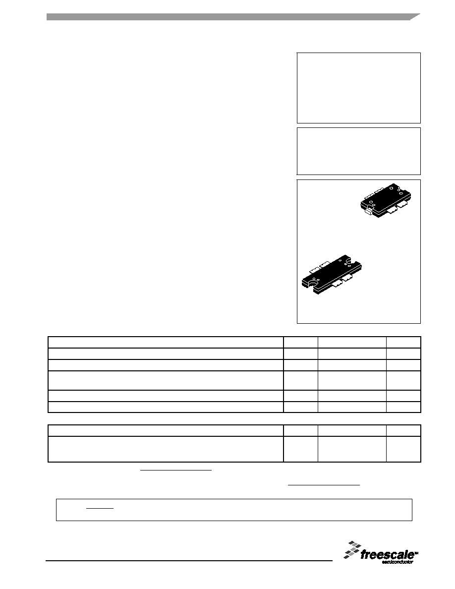
CASE 1486-03, STYLE 1
TO-270 WB-4
PLASTIC
MRF5S9101NR1(MR1)
CASE 1484-02, STYLE 1
TO-272 WB-4
PLASTIC
MRF5S9101NBR1(MBR1)
Freescale Semiconductor, Inc., 2005. All rights reserved.
2
RF Device Data
Freescale Semiconductor
MRF5S9101NR1 MRF5S9101NBR1 MRF5S9101MR1 MRF5S9101MBR1
Table 3. ESD Protection Characteristics
Test Methodology
Class
Human Body Model (per JESD22-A114)
1C (Minimum)
Machine Model (per EIA/JESD22-A115)
A (Minimum)
Charge Device Model (per JESD22-C101)
IV (Minimum)
Table 4. Moisture Sensitivity Level
Test Methodology
Rating
Package Peak Temperature
Unit
Per JESD 22-A113, IPC/JEDEC J-STD-020
3
260
∞C
Table 5. Electrical Characteristics
(T
C
= 25∞C unless otherwise noted)
Characteristic
Symbol
Min
Typ
Max
Unit
Zero Gate Voltage Drain Leakage Current
(V
DS
= 68 Vdc, V
GS
= 0 Vdc)
I
DSS
--
--
10
µAdc
Zero Gate Voltage Drain Leakage Current
(V
DS
= 26 Vdc, V
GS
= 0 Vdc)
I
DSS
--
--
1
µAdc
Gate-Source Leakage Current
(V
GS
= 5 Vdc, V
DS
= 0 Vdc)
I
GSS
--
--
1
µAdc
On Characteristics
Gate Threshold Voltage
(V
DS
= 10 Vdc, I
D
= 400 µAdc)
V
GS(th)
2
2.8
3.5
Vdc
Gate Quiescent Voltage
(V
DS
= 26 Vdc, I
D
= 700 mAdc)
V
GS(Q)
--
3.7
--
Vdc
Drain-Source On-Voltage
(V
GS
= 10 Vdc, I
D
= 2
Adc)
V
DS(on)
--
0.21
0.3
Vdc
Forward Transconductance
(V
DS
= 10 Vdc, I
D
= 6
Adc)
g
fs
--
7
--
S
Dynamic Characteristics
(1)
Output Capacitance
(V
DS
= 26 Vdc ± 30 mV(rms)ac @ 1 MHz, V
GS
= 0 Vdc)
C
oss
--
70
--
pF
Reverse Transfer Capacitance
(V
DS
= 26
Vdc ± 30 mV(rms)ac @ 1 MHz, V
GS
= 0 Vdc)
C
rss
--
2.2
--
pF
Functional Tests (In Freescale Test Fixture, 50 ohm system) V
DD
= 26 Vdc, P
out
= 100 W, I
DQ
= 700 mA, f = 960 MHz
Power Gain
G
ps
16
17.5
19
dB
Drain Efficiency
D
56
60
--
%
Input Return Loss
IRL
--
-15
-9
dB
P
out
@ 1 dB Compression Point, CW
P1dB
100
110
--
W
1. Part is internally input matched.
(continued)

MRF5S9101NR1 MRF5S9101NBR1 MRF5S9101MR1 MRF5S9101MBR1
3
RF Device Data
Freescale Semiconductor
Table 5. Electrical Characteristics
(T
C
= 25∞C unless otherwise noted)
(continued)
Characteristic
Symbol
Min
Typ
Max
Unit
Typical GSM EDGE Performances (In Freescale GSM EDGE Test Fixture, 50 hm system) V
DD
= 28 Vdc, P
out
= 50 W Avg.,
I
DQ
= 650 mA, 869 MHz<Frequency<894 MHz, 920 MHz<Frequency<960 MHz
Power Gain
G
ps
--
18
--
dB
Drain Efficiency
D
--
42
--
%
Error Vector Magnitude
EVM
--
2.3
--
% rms
Spectral Regrowth at 400 kHz Offset
SR1
--
-63
--
dBc
Spectral Regrowth at 600 kHz Offset
SR2
--
-78
--
dBc
4
RF Device Data
Freescale Semiconductor
MRF5S9101NR1 MRF5S9101NBR1 MRF5S9101MR1 MRF5S9101MBR1
Z1
0.698 x 0.827 Microstrip
Z2
0.720 x 0.788 Microstrip
Z3
0.195 x 0.087 Microstrip
Z4
0.524 x 0.087 Microstrip
Z5
0.233 x 0.087 Microstrip
Z6
0.560 x 0.087 Microstrip
Z7
0.095 x 0.827 Microstrip
Z8
0.472 x 0.087 Microstrip
Z9
0.384 x 0.087 Microstrip
Z10
1.491 x 0.087 Microstrip
Z11, Z12*
1.6 x 0.089 Microstrip
(quarter wave length for supply purpose)
Z13*
1.2 x 0.059 Microstrip
(quarter wave length for bias purpose)
PCB
Taconic TLX8-0300, 0.030,
r
= 2.55
*Variable for tuning
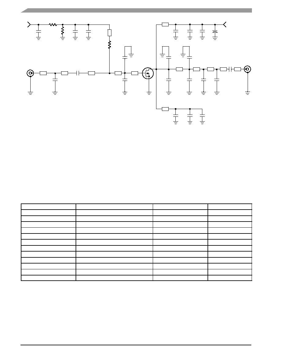
Figure 1. MRF5S9101NR1(NBR1)/MR1(MBR1) 900 MHz Test Circuit Schematic
RF
INPUT
RF
OUTPUT
C1
C10
V
SUPPLY
Z6
V
BIAS
Z10
Z4
C11
C21
+
C7
C19
C8
C2
C5
Z2
C18
C20
C13
C16
C12
Z1
DUT
Z8
R1
C4
R2
Z13
R3
C17
Z11
C9
C3
C6
Z12
C14
C15
Z5
Z9
Z7
Z3
Table 6. MRF5S9101NR1(NBR1)/MR1(MBR1) 900 MHz Test Circuit Component Designations and Values
Part
Description
Part Number
Manufacturer
C1, C2, C3
4.7 mF Chip Capacitors (2220)
GRM55ER7H475KA01
Murata
C4, C5, C6
10 nF 200B Chip Capacitors
200B103MW
ATC
C7, C8, C9
33 pF 100B Chip Capacitors
100B330JW
ATC
C10, C11
22 pF 100B Chip Capacitors
100B220GW
ATC
C12, C13
10 pF 100B Chip Capacitors
100B100GW
ATC
C14, C15, C16, C17
8.2 pF 100B Chip Capacitors
100B8R2CW
ATC
C18
5.6 pF 100B Chip Capacitor
100B5R6CW
ATC
C19
4.7 pF 100B Chip Capacitor
100B4R7BW
ATC
C20
3.9 pF 100B Chip Capacitor
100B3R9BW
ATC
C21
220 mF, 50 V Electrolytic Capacitor, Axial
516D227M050NP7B
Sprague
R1, R2
10 kW, 1/4 W Chip Resistors (1206)
R3
10 W, 1/4 W Chip Resistor (1206)
MRF5S9101NR1 MRF5S9101NBR1 MRF5S9101MR1 MRF5S9101MBR1
5
RF Device Data
Freescale Semiconductor
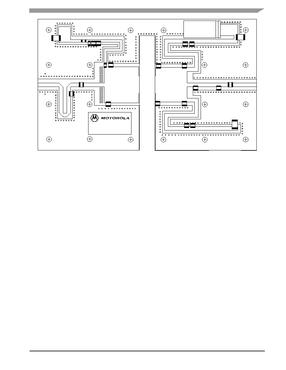
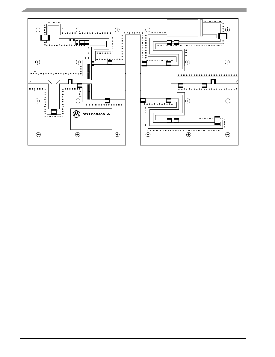
Figure 2. MRF5S9101NR1(NBR1)/MR1(MBR1) 900 MHz Test Circuit Component Layout
C10
C12
C15
C11
C20
C13
C1
C2
C8
C9
C14
C16
C17
C19
R3
R1
C18
VGG
R2
C7
C21
C5
C3
C6
VDD
C4
CUT
OUT
AREA
Rev 2
MRF5S9101N
900 MHz
Freescale has begun the transition of marking Printed Circuit Boards (PCBs) with the Freescale Semiconductor
signature/logo. PCBs may have either Motorola or Freescale markings during the transition period. These changes will have
no impact on form, fit or function of the current product.
6
RF Device Data
Freescale Semiconductor
MRF5S9101NR1 MRF5S9101NBR1 MRF5S9101MR1 MRF5S9101MBR1
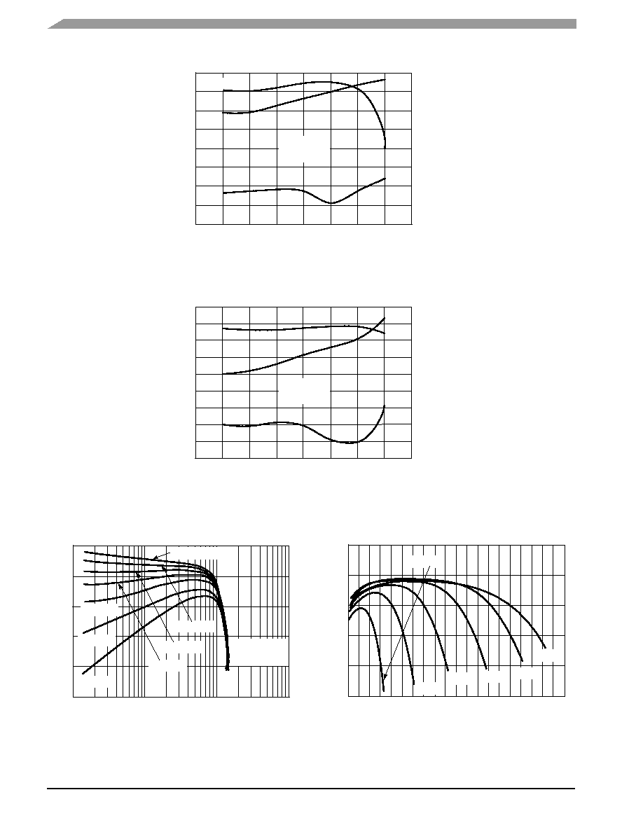
TYPICAL CHARACTERISTICS - 900 MHz
1020
10
18
860
- 45
70
60
17
50
16
40
15
30
14
0
13
12
- 15
11
- 30
880
900
920
940
960
980
1000
G
ps
, POWER GAIN (dB)
INPUT
RETURN LOSS (dB)
IRL,
f, FREQUENCY (MHz)
Figure 3. Power Gain, Input Return Loss and Drain
Efficiency versus Frequency @ P
out
= 100 Watts CW
IRL
G
ps
V
DD
= 26 Vdc
I
DQ
= 700 mA
1020
10
19
860
- 24
50
45
17
35
16
30
15
14
- 8
13
12
- 16
11
- 20
880
900
920
940
960
980
1000
G
ps
, POWER GAIN (dB)
IRL
G
ps
V
DD
= 26 Vdc
I
DQ
= 700 mA
f, FREQUENCY (MHz)
Figure 4. Power Gain, Input Return Loss and Drain
Efficiency versus Frequency @ P
out
= 40 Watts CW
18
- 12
40
1000
14
19
1
I
DQ
= 1500 mA
1300 mA
P
out
, OUTPUT POWER (WATTS)
Figure 5. Power Gain versus Output Power
G
ps
, POWER GAIN (dB)
V
DD
= 26 Vdc
f = 940 MHz
1100 mA
900 mA
700 mA
500 mA
300 mA
18
17
16
15
10
100
200
14
19
0
P
out
, OUTPUT POWER (WATTS) CW
Figure 6. Power Gain versus Output Power
G
ps
, POWER GAIN (dB)
V
DD
= 12 V
16 V
24 V
28 V
32 V
18
17
16
15
20
40
60
80
100
120
140
160
180
20 V
D
, DRAIN EFFICIENCY (%)
INPUT
RETURN LOSS (dB)
IRL,
D
, DRAIN EFFICIENCY (%)
D
D
MRF5S9101NR1 MRF5S9101NBR1 MRF5S9101MR1 MRF5S9101MBR1
7
RF Device Data
Freescale Semiconductor
TYPICAL CHARACTERISTICS - 900 MHz
1000
1
0
70
G
ps
T
C
= - 30
_C
P
out
, OUTPUT POWER (WATTS) CW
Figure 7. Power Gain and Drain Efficiency
versus CW Output Power
G
ps
, POWER GAIN (dB)
V
DD
= 26 Vdc
I
DQ
= 700 mA
f = 940 MHz
25
_C
85
_C
T
C
= - 30
_C
25
_C
85
_C
100
10
60
50
40
30
20
10
13
20
19
18
17
16
15
14
980
0
3.5
900
P
out
= 50 W Avg.
f, FREQUENCY (MHz)
Figure 8. Error Vector Magnitude versus
Frequency
EVM, ERROR VECT
OR MAGNITUDE (% rms)
V
DD
= 28 Vdc
I
DQ
= 650 mA
40 W Avg.
25 W Avg.
3
2.5
2
1.5
1
0.5
910
920
930
940
950
960
970
D
100
0
9
1
0
60
EVM
P
out
, OUTPUT POWER (WATTS) AVG.
Figure 9. Error Vector Magnitude and Drain
Efficiency versus Output Power
EVM, ERROR VECT
OR MAGNITUDE (% rms)
T
C
= 85
_C
25
_C
- 30
_C
V
DD
= 28 Vdc
I
DQ
= 650 mA
f = 940 MHz
8
50
6
40
5
30
3
20
2
10
10
980
- 83
- 63
900
SR 400 kHz
f, FREQUENCY (MHz)
Figure 10. Spectral Regrowth at 400 kHz and
600 kHz versus Frequency
SPECTRAL
REGROWTH @ 400 kHz and 600 kHz (dBc)
V
DD
= 28 Vdc
I
DQ
= 650 mA
f = 940 MHz
- 68
- 73
- 78
910
920
930
940
950
960
970
P
out
= 50 W Avg.
SR 600 kHz
25 W Avg.
40 W Avg.
25 W Avg.
40 W Avg.
50 W Avg.
90
- 80
- 45
0
T
C
= 85
_C
P
out
, OUTPUT POWER (WATTS) AVG.
Figure 11. Spectral Regrowth at 400 kHz
versus Output Power
SPECTRAL
REGROWTH @ 400 kHz (dBc)
25
_C
- 30
_C
- 60
- 65
- 70
10
20
30
40
50
60
70
80
- 50
- 55
- 75
V
DD
= 28 Vdc
I
DQ
= 650 mA
f = 940 MHz
D
, DRAIN EFFICIENCY (%)
D
, DRAIN EFFICIENCY (%)
D
8
RF Device Data
Freescale Semiconductor
MRF5S9101NR1 MRF5S9101NBR1 MRF5S9101MR1 MRF5S9101MBR1
TYPICAL CHARACTERISTICS - 900 MHz
90
- 85
- 65
0
T
C
= 85
_C
P
out
, OUTPUT POWER (WATTS) AVG.
Figure 12. Spectral Regrowth @ 600 kHz
versus Output Power
SPECTRAL
REGROWTH @ 600 kHz (dBc)
25
_C
- 30
_C
- 70
- 75
- 80
10
20
30
40
50
60
70
80
V
DD
= 28 Vdc
I
DQ
= 650 mA
f = 940 MHz
T
J
, JUNCTION TEMPERATURE (
∞C)
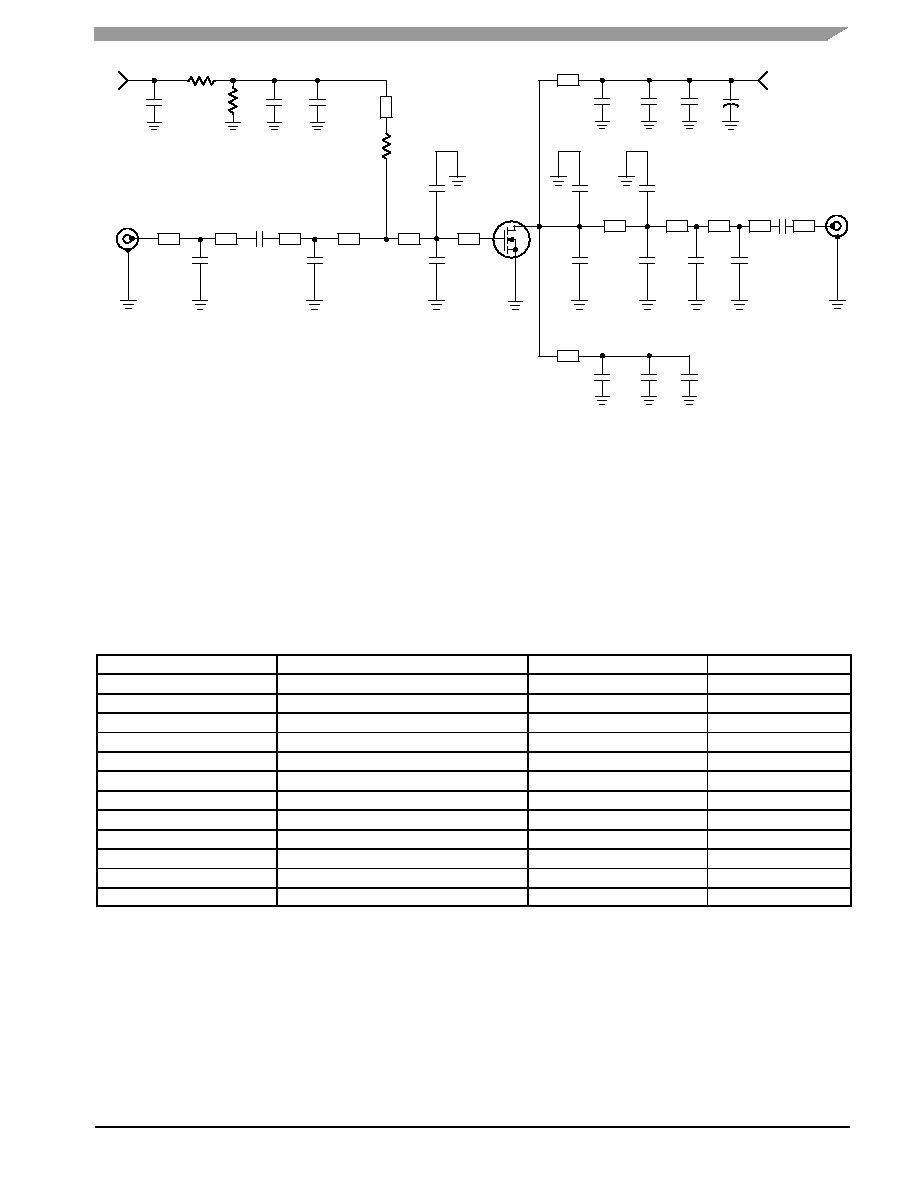
This above graph displays calculated MTTF in hours x ampere
2
drain current. Life tests at elevated temperatures have correlated to
better than
±10% of the theoretical prediction for metal failure. Divide
MTTF factor by I
D
2
for MTTF in a particular application.
Figure 13. MTTF Factor versus Junction Temperature
210
1.E+07
1.E+10
90
MTTF F
ACT
OR (HOURS X AMPS
2
)
1.E+09
1.E+08
100 110 120 130 140 150 160 170 180 190 200
MRF5S9101NR1 MRF5S9101NBR1 MRF5S9101MR1 MRF5S9101MBR1
9
RF Device Data
Freescale Semiconductor
Figure 14. MRF5S9101NR1(NBR1)/MR1(MBR1) 800 MHz Test Circuit Schematic
Z1
0.432 x 0.827 Microstrip
Z2
0.720 x 0.788 Microstrip
Z3
0.195 x 0.087 Microstrip
Z4
0.584 x 0.087 Microstrip
Z5
0.173 x 0.087 Microstrip
Z6
0.560 x 0.087 Microstrip
Z7
0.378 x 0.827 Microstrip
Z8
0.279 x 0.087 Microstrip
Z9
0.193 x 0.087 Microstrip
Z10
0.897 x 0.087 Microstrip
Z11
1.161 x 0.087 Microstrip
Z12, Z13*
1.6 x 0.089 Microstrip
(quarter wave length for supply purpose)
Z14*
1.2 x 0.059 Microstrip
(quarter wave length for bias purpose)
PCB
Taconic TLX8-0300, 0.030,
r
= 2.55
*Variable for tuning
RF
INPUT
RF
OUTPUT
C1
C10
V
SUPPLY
Z6
V
BIAS
Z11
C11
C21
+
C7
C19
C8
C2
C5
Z2
C13
C16
C12
Z1
DUT
Z8
R1
C4
R2
Z14
R3
C17
Z12
C9
C3
C6
Z13
C14
C15
C22
Z3
Z5
Z4
C18
C20
Z7
Z10
Z9
Table 7. MRF5S9101NR1(NBR1)/MR1(MBR1) 800 MHz Test Circuit Component Designations and Values
Part
Description
Part Number
Manufacturer
C1, C2, C3
4.7 mF Chip Capacitors (2220)
GRM55ER7H475KA01
Murata
C4, C5, C6
10 nF 200B Chip Capacitors
200B103MW
ATC
C7, C8, C9
33 pF 100B Chip Capacitors
100B330JW
ATC
C10, C11
22 pF 100B Chip Capacitors
100B220GW
ATC
C12, C13, C17
10 pF 100B Chip Capacitors
100B100GW
ATC
C14, C15
8.2 pF 100B Chip Capacitors
100B8R2CW
ATC
C16, C22
6.8 pF 100B Chip Capacitors
100B6R8CW
ATC
C18
5.6 pF 100B Chip Capacitor
100B5R6CW
ATC
C19, C20
2.7 pF 100B Chip Capacitors
100B2R7BW
ATC
C21
220 mF, 50 V Electrolytic Capacitor, Axial
516D227M050NP7B
Sprague
R1, R2
10 kW, 1/4 W Chip Resistors (1206)
R3
10 W, 1/4 W Chip Resistor (1206)
10
RF Device Data
Freescale Semiconductor
MRF5S9101NR1 MRF5S9101NBR1 MRF5S9101MR1 MRF5S9101MBR1
Figure 15. MRF5S9101NR1(NBR1)/MR1(MBR1) 800 MHz Test Circuit Component Layout
CUT
OUT
AREA
C1
VGG
800 MHz
MRF5S9101N
Rev 2
VDD
R2
R1
C4 C7
R3
C16
C17
C10
C22
C19
C21
C8
C5
C2
C14
C13
C11
C18
C20
C12
C15
C9
C6
C3
Freescale has begun the transition of marking Printed Circuit Boards (PCBs) with the Freescale Semiconductor
signature/logo. PCBs may have either Motorola or Freescale markings during the transition period. These changes will have
no impact on form, fit or function of the current product.
MRF5S9101NR1 MRF5S9101NBR1 MRF5S9101MR1 MRF5S9101MBR1
11
RF Device Data
Freescale Semiconductor
TYPICAL CHARACTERISTICS - 800 MHz
940
10
20
820
- 20
65
19
60
18
55
17
50
16
45
15
- 10
14
- 12
13
- 14
12
- 16
11
- 18
830 840 850 860 870 880 890 900 910 920 930
f, FREQUENCY (MHz)
Figure 16. Power Gain, Input Return Loss and Drain
Efficiency versus Frequency @ P
out
= 100 W CW
G
ps
, POWER GAIN (dB)
IRL
G
ps
V
DD
= 26 Vdc
I
DQ
= 700 mA
940
10
20
820
- 20
45
IRL
G
ps
f, FREQUENCY (MHz)
Figure 17. Power Gain, Input Return Loss and Drain
Efficiency versus Frequency @ P
out
= 40 W CW
G
ps
, POWER GAIN (dB)
V
DD
= 26 Vdc
I
DQ
= 700 mA
19
40
18
35
17
30
16
25
15
- 10
14
- 12
13
- 14
12
- 16
11
- 18
830 840 850 860 870 880 890 900 910 920 930
910
0
3.5
850
P
out
= 50 W Avg.
f, FREQUENCY (MHz)
Figure 18. Error Vector Magnitude versus
Frequency
V
DD
= 28 Vdc
I
DQ
= 650 mA
EVM, ERROR VECT
OR MAGNITUDE (% rms)
3
2.5
2
1.5
1
0.5
860
860
870
880
890
900
40 W Avg.
25 W Avg.
100
0
9
1
0
60
P
out
, OUTPUT POWER (WATTS) AVG.
Figure 19. Error Vector Magnitude and Drain
Efficiency versus Output Power
V
DD
= 28 Vdc
I
DQ
= 650 mA
f = 880 MHz
EVM
, DRAIN EFFICIENCY
(%)
EVM, ERROR VECT
OR MAGNITUDE (% rms)
8
50
6
40
5
30
3
20
2
10
10
T
C
= 25
_C
INPUT
RETURN LOSS (dB)
IRL,
D
, DRAIN EFFICIENCY (%)
D
INPUT
RETURN LOSS (dB)
IRL,
D
, DRAIN EFFICIENCY (%)
D
12
RF Device Data
Freescale Semiconductor
MRF5S9101NR1 MRF5S9101NBR1 MRF5S9101MR1 MRF5S9101MBR1
TYPICAL CHARACTERISTICS - 800 MHz
910
- 82
- 64
850
SR 400 kHz
P
out
= 50 W Avg.
f, FREQUENCY (MHz)
Figure 20. Spectral Regrowth at 400 kHz and
600 kHz versus Frequency
SPECTRAL
REGROWTH @ 400 kHz
AND 600 kHz (dBc)
SR 600 kHz
40 W Avg.
25 W Avg.
P
out
= 50 W Avg.
40 W Avg.
25 W Avg.
- 66
- 68
- 70
- 72
- 74
- 76
- 78
- 80
860
870
880
900
890
V
DD
= 28 Vdc
I
DQ
= 650 mA
90
- 80
- 45
0
T
C
= 25
_C
P
out
, OUTPUT POWER (WATTS) AVG.
Figure 21. Spectral Regrowth at 400 kHz
versus Output Power
V
DD
= 28 Vdc
I
DQ
= 650 mA
f = 880 MHz
SPECTRAL
REGROWTH @ 400 kHz (dBc)
10
20
30
40
50
60
70
80
- 50
- 55
- 60
- 65
- 70
- 75
90
- 85
- 65
0
T
C
= 25
_C
P
out
, OUTPUT POWER (WATTS) AVG.
Figure 22. Spectral Regrowth at 600 kHz
versus Output Power
V
DD
= 28 Vdc
I
DQ
= 650 mA
f = 880 MHz
SPECTRAL
REGROWTH @ 400 kHz (dBc)
- 70
- 75
- 80
10
20
30
40
50
60
70
80
MRF5S9101NR1 MRF5S9101NBR1 MRF5S9101MR1 MRF5S9101MBR1
13
RF Device Data
Freescale Semiconductor
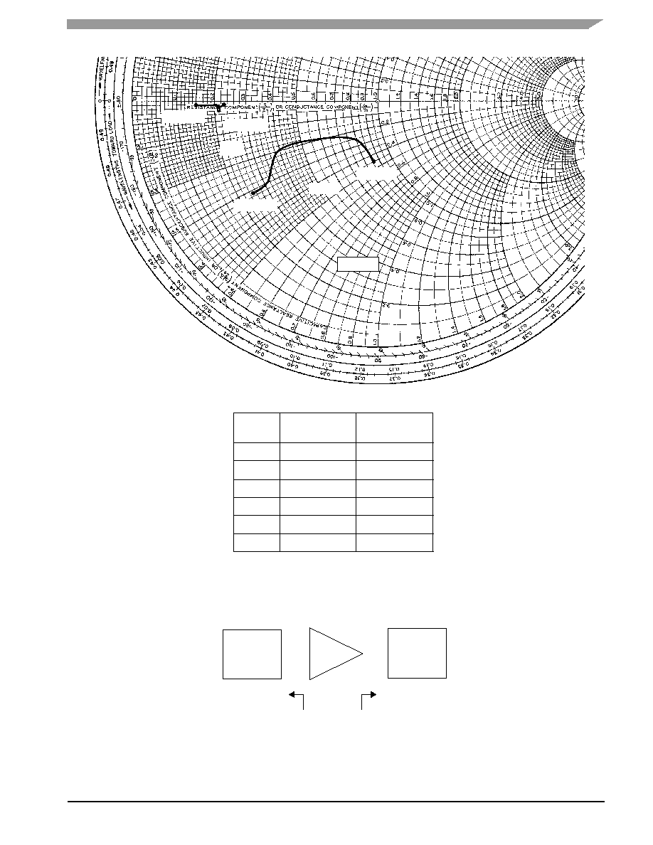
Figure 23. Series Equivalent Source and Load Impedance
f
MHz
Z
source
Z
load
845
865
4.29 - j2.23
2.72 - j0.96
3.94 - j1.24
1.15 - j0.04
1.05 - j0.10
1.02 - j0.07
V
DD
=
26 Vdc, I
DQ
= 700 mA, P
out
= 100 W CW
Z
o
= 5
f = 990 MHz
f = 990 MHz
f = 845 MHz
f = 845 MHz
890
920
1.96 - j1.02
1.03 - j0.15
Z
load
Z
source
Z
source
= Test circuit impedance as measured from
gate to ground.
Z
load
= Test circuit impedance as measured
from drain to ground.
Z source
Z load
Input
Matching
Network
Device
Under Test
Output
Matching
Network
1.58 - j1.43
1.03 - j0.05
960
990
1.27 - j1.54
0.73 - j0.07

14
RF Device Data
Freescale Semiconductor
MRF5S9101NR1 MRF5S9101NBR1 MRF5S9101MR1 MRF5S9101MBR1
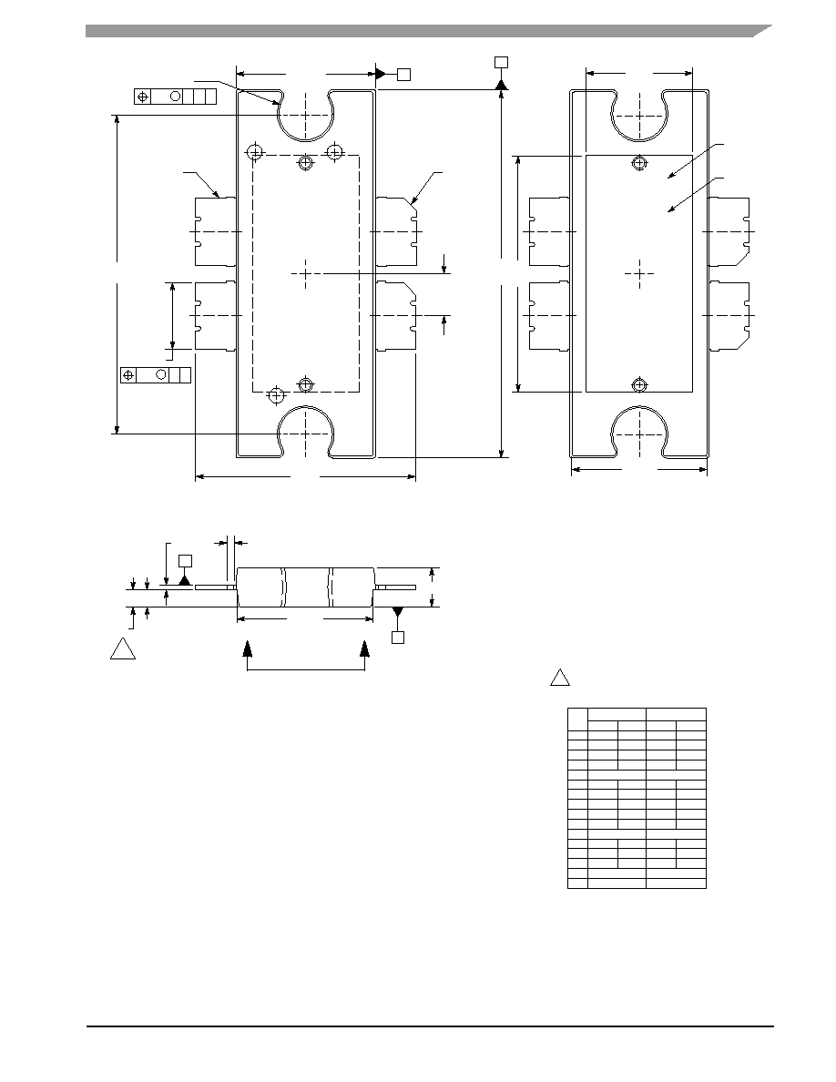
PACKAGE DIMENSIONS
CASE 1486-03
ISSUE C
DATUM
PLANE
BOTTOM VIEW
A1
2X
D1
E3
E1
D3
E4
A2
PIN 5
NOTE 8
A
B
C
H
DRAIN LEAD
D
A
M
aaa
C
4X
b1
2X
D2
NOTES:
1. CONTROLLING DIMENSION: INCH.
2. INTERPRET DIMENSIONS AND TOLERANCES
PER ASME Y14.5M-1994.
3. DATUM PLANE -H- IS LOCATED AT THE TOP OF
LEAD AND IS COINCIDENT WITH THE LEAD
WHERE THE LEAD EXITS THE PLASTIC BODY AT
THE TOP OF THE PARTING LINE.
4. DIMENSIONS
"D" AND "E1" DO NOT INCLUDE
MOLD PROTRUSION. ALLOWABLE PROTRUSION
IS .006 PER SIDE. DIMENSIONS
"D" AND "E1" DO
INCLUDE MOLD MISMATCH AND ARE DETER-
MINED AT DATUM PLANE -H-.
5. DIMENSION
"b1" DOES NOT INCLUDE DAMBAR
PROTRUSION. ALLOWABLE DAMBAR
PROTRUSION SHALL BE .005 TOTAL IN EXCESS
OF THE
"b1" DIMENSION AT MAXIMUM MATERIAL
CONDITION.
6. DATUMS -A- AND -B- TO BE DETERMINED AT
DATUM PLANE -H-.
7. DIMENSION A2 APPLIES WITHIN ZONE
"J" ONLY.
8. HATCHING REPRESENTS THE EXPOSED AREA
OF THE HEAT SLUG.
c1
F
ZONE J
E2
2X
A
DIM
A
MIN
MAX
MIN
MAX
MILLIMETERS
.100
.104
2.54
2.64
INCHES
A1
.039
.043
0.99
1.09
A2
.040
.042
1.02
1.07
D
.712
.720
18.08
18.29
D1
.688
.692
17.48
17.58
D2
.011
.019
0.28
0.48
D3
.600
- - -
15.24
- - -
E
.551
.559
14
14.2
E1
.353
.357
8.97
9.07
E2
.132
.140
3.35
3.56
E3
.124
.132
3.15
3.35
E4
.270
- - -
6.86
- - -
F
b1
.164
.170
4.17
4.32
c1
.007
.011
0.18
0.28
e
.025 BSC
.106 BSC
0.64 BSC
2.69 BSC
1
STYLE 1:
PIN 1. DRAIN
2. DRAIN
3. GATE
4. GATE
5. SOURCE
aaa
.004
0.10
GATE LEAD
4X
e
2X
E
SEATING
PLANE
4
2
3
««««««
««««««
««««««
««««««
««««««
««««««
««««««
««««««
««««««
««««««
««««««
««««««
««««««
NOTE 7
E5
E5
E5
.346
.350
8.79
8.89
TO-270 WB-4
PLASTIC
MRF5S9101NR1(MR1)
MRF5S9101NR1 MRF5S9101NBR1 MRF5S9101MR1 MRF5S9101MBR1
15
RF Device Data
Freescale Semiconductor
TO-272 WB-4
PLASTIC
MRF5S9101NBR1(MBR1)
…………………
…………………
…………………
…………………
…………………
…………………
…………………
…………………
…………………
…………………
…………………
…………………
CASE 1484-02
ISSUE B
NOTES:
1. CONTROLLING DIMENSION: INCH.
2. INTERPRET DIMENSIONS AND TOLERANCES PER
ASME Y14.5M-1994.
3. DATUM PLANE -H- IS LOCATED AT TOP OF LEAD
AND IS COINCIDENT WITH THE LEAD WHERE THE
LEAD EXITS THE PLASTIC BODY AT THE TOP OF
THE PARTING LINE.
4. DIMENSIONS "D" AND "E1" DO NOT INCLUDE
MOLD PROTRUSION. ALLOWABLE PROTRUSION
IS .006 PER SIDE. DIMENSIONS "D" AND "E1" DO
INCLUDE MOLD MISMATCH AND ARE
DETERMINED AT DATUM PLANE -H-.
5. DIMENSION "b1" DOES NOT INCLUDE DAMBAR
PROTRUSION. ALLOWABLE DAMBAR
PROTRUSION SHALL BE .005 TOTAL IN EXCESS
OF THE "b1" DIMENSION AT MAXIMUM MATERIAL
CONDITION.
6. DATUMS -A- AND -B- TO BE DETERMINED AT
DATUM PLANE -H-.
7. DIMENSION A2 APPLIES WITHIN ZONE "J" ONLY.
8. HATCHING REPRESENTS THE EXPOSED AREA OF
THE HEAT SLUG.
DATUM
PLANE
Y
Y
DIM
A
MIN
MAX
MIN
MAX
MILLIMETERS
.100
.104
2.54
2.64
INCHES
D2
.600
- - -
15.24
- - -
E2
.270
- - -
6.86
- - -
D
.928
.932
23.57
23.67
D1
E
.551
.559
14
14.2
E1
.353
.357
8.97
9.07
b1
.164
.170
4.17
4.32
c1
.007
.011
.18
.28
e
r1
.063
.068
1.60
1.73
aaa
.106 BSC
.004
2.69 BSC
.10
B
A
E1
D
4X
b1
D1
E
GATE LEAD
M
aaa
C A
M
aaa
C A
D2
E2
VIEW Y-Y
4X
e
A1
.039
.043
0.99
1.09
F
A2
.040
.042
1.02
1.07
.025 BSC
0.64 BSC
A1
C
H
c1
A
ZONE J
SEATING
PLANE
.810 BSC
20.57 BSC
PIN 5
2X
r1
B
DRAIN LEAD
F
A2
7
NOTE 8
1
2
3
4
STYLE 1:
PIN 1. DRAIN
2. DRAIN
3. GATE
4. GATE
5. SOURCE
E3
E3
E3
.346
.350
8.79
8.89

16
RF Device Data
Freescale Semiconductor
MRF5S9101NR1 MRF5S9101NBR1 MRF5S9101MR1 MRF5S9101MBR1
Information in this document is provided solely to enable system and software
implementers to use Freescale Semiconductor products. There are no express or
implied copyright licenses granted hereunder to design or fabricate any integrated
circuits or integrated circuits based on the information in this document.
Freescale Semiconductor reserves the right to make changes without further notice to
any products herein. Freescale Semiconductor makes no warranty, representation or
guarantee regarding the suitability of its products for any particular purpose, nor does
Freescale Semiconductor assume any liability arising out of the application or use of
any product or circuit, and specifically disclaims any and all liability, including without
limitation consequential or incidental damages. "Typical" parameters that may be
provided in Freescale Semiconductor data sheets and/or specifications can and do
vary in different applications and actual performance may vary over time. All operating
parameters, including "Typicals", must be validated for each customer application by
customer's technical experts. Freescale Semiconductor does not convey any license
under its patent rights nor the rights of others. Freescale Semiconductor products are
not designed, intended, or authorized for use as components in systems intended for
surgical implant into the body, or other applications intended to support or sustain life,
or for any other application in which the failure of the Freescale Semiconductor product
could create a situation where personal injury or death may occur. Should Buyer
purchase or use Freescale Semiconductor products for any such unintended or
unauthorized application, Buyer shall indemnify and hold Freescale Semiconductor
and its officers, employees, subsidiaries, affiliates, and distributors harmless against all
claims, costs, damages, and expenses, and reasonable attorney fees arising out of,
directly or indirectly, any claim of personal injury or death associated with such
unintended or unauthorized use, even if such claim alleges that Freescale
Semiconductor was negligent regarding the design or manufacture of the part.
Freescalet and the Freescale logo are trademarks of Freescale Semiconductor, Inc.
All other product or service names are the property of their respective owners.
Freescale Semiconductor, Inc. 2005. All rights reserved.
How to Reach Us:
Home Page:
www.freescale.com
E-mail:
support@freescale.com
USA/Europe or Locations Not Listed:
Freescale Semiconductor
Technical Information Center, CH370
1300 N. Alma School Road
Chandler, Arizona 85224
+1-800-521-6274 or +1-480-768-2130
support@freescale.com
Europe, Middle East, and Africa:
Freescale Halbleiter Deutschland GmbH
Technical Information Center
Schatzbogen 7
81829 Muenchen, Germany
+44 1296 380 456 (English)
+46 8 52200080 (English)
+49 89 92103 559 (German)
+33 1 69 35 48 48 (French)
support@freescale.com
Japan:
Freescale Semiconductor Japan Ltd.
Headquarters
ARCO Tower 15F
1-8-1, Shimo-Meguro, Meguro-ku,
Tokyo 153-0064
Japan
0120 191014 or +81 3 5437 9125
support.japan@freescale.com
Asia/Pacific:
Freescale Semiconductor Hong Kong Ltd.
Technical Information Center
2 Dai King Street
Tai Po Industrial Estate
Tai Po, N.T., Hong Kong
+800 2666 8080
support.asia@freescale.com
For Literature Requests Only:
Freescale Semiconductor Literature Distribution Center
P.O. Box 5405
Denver, Colorado 80217
1-800-441-2447 or 303-675-2140
Fax: 303-675-2150
LDCForFreescaleSemiconductor@hibbertgroup.com
Document Number: MRF5S9101
Rev. 2, 7/2005