MRF6P3300HR3 MRF6P3300HR5
1
RF Device Data
Freescale Semiconductor
RF Power Field Effect Transistor
N-Channel Enhancement-Mode Lateral MOSFET
Designed for broadband commercial and industrial applications with
frequencies from 470 to 860 MHz. The high gain and broadband performance
of this device make it ideal for large - signal, common - source amplifier
applications in 32 volt analog or digital television transmitter equipment.
∑ Typical Narrowband Two-Tone Performance @ 860 MHz: V
DD
= 32 Volts,
I
DQ
= 1600 mA, P
out
= 270 Watts PEP
Power Gain -- 20.2 dB
Drain Efficiency -- 44.1%
IMD -- -30.8 dBc
∑ Typical Narrowband DVBT OFDM Performance @ 860 MHz: V
DD
=
32 Volts, I
DQ
= 1600 mA, P
out
= 60 Watts Avg., 8K Mode, 64 QAM
Power Gain -- 20.4 dB
Drain Efficiency -- 29%
ACPR @ 3.9 MHz Offset -- -57 dBc @ 20 kHz Bandwidth
∑ Capable of Handling 10:1 VSWR, @ 32 Vdc, 860 MHz, 300 Watts CW
Output Power
∑ Characterized with Series Equivalent Large-Signal Impedance Parameters
∑ Internally Matched for Ease of Use
∑ Designed for Push-Pull Operation Only
∑ Qualified Up to a Maximum of 32 V
DD
Operation
∑ Integrated ESD Protection
∑ Lower Thermal Resistance Package
∑ Low Gold Plating Thickness on Leads, 40
µ
Nominal.
∑ Pb-Free and RoHS Compliant
∑ In Tape and Reel. R3 Suffix = 250 Units per 56 mm, 13 inch Reel.
R5 Suffix = 50 Units per 56 mm, 13 inch Reel.
Table 1. Maximum Ratings
Rating
Symbol
Value
Unit
Drain-Source Voltage
V
DSS
-0.5, +68
Vdc
Gate-Source Voltage
V
GS
-0.5, +12
Vdc
Total Device Dissipation @ T
C
= 25∞C
Derate above 25∞C
P
D
761
4.3
W
W/∞C
Storage Temperature Range
T
stg
- 65 to +150
∞C
Operating Junction Temperature
T
J
200
∞C
Table 2. Thermal Characteristics
Characteristic
Symbol
Value
(1,2)
Unit
Thermal Resistance, Junction to Case
Case Temperature 80∞C, 300 W CW
Case Temperature 82∞C, 220 W CW
Case Temperature 79∞C, 100 W CW
Case Temperature 81∞C, 60 W CW
R
JC
0.23
0.24
0.27
0.27
∞C/W
1. MTTF calculator available at http://www.freescale.com/rf. Select Tools/Software/Application Software/Calculators to
access the MTTF calculators by product.
2. Refer to AN1955, Thermal Measurement Methodology of RF Power Amplifiers. Go to http://www.freescale.com/rf.
Select Documentation/Application Notes - AN1955.
NOTE - CAUTION - MOS devices are susceptible to damage from electrostatic charge. Reasonable precautions in handling and
packaging MOS devices should be observed.
Document Number: MRF6P3300H
Rev. 0, 9/2005
Freescale Semiconductor
Technical Data
MRF6P3300HR3
MRF6P3300HR5
470-860 MHz, 300 W, 32 V
LATERAL N-CHANNEL
RF POWER MOSFET
CASE 375G-04, STYLE 1
NI-860C3
Freescale Semiconductor, Inc., 2005. All rights reserved.
2
RF Device Data
Freescale Semiconductor
MRF6P3300HR3 MRF6P3300HR5
Table 3. ESD Protection Characteristics
Test Methodology
Class
Human Body Model (per JESD22-A114)
3B (Minimum)
Machine Model (per EIA/JESD22-A115)
C (Minimum)
Charge Device Model (per JESD22-C101)
IV (Minimum)
Table 4. Electrical Characteristics
(T
C
= 25∞C unless otherwise noted)
Characteristic
Symbol
Min
Typ
Max
Unit
Off Characteristics
(1)
Zero Gate Voltage Drain Leakage Current
(V
DS
= 68 Vdc, V
GS
= 0 Vdc)
I
DSS
--
--
10
µAdc
Zero Gate Voltage Drain Leakage Current
(V
DS
= 32 Vdc, V
GS
= 0 Vdc)
I
DSS
--
--
1
µAdc
Gate-Source Leakage Current
(V
GS
= 5 Vdc, V
DS
= 0 Vdc)
I
GSS
--
--
1
µAdc
On Characteristics
(1)
Gate Threshold Voltage
(V
DS
= 10 Vdc, I
D
= 350 µAdc)
V
GS(th)
1
2.2
3
Vdc
Drain-Source On-Voltage
(V
GS
= 10 Vdc, I
D
= 2.4 Adc)
V
DS(on)
--
0.22
0.3
Vdc
Forward Transconductance
(V
DS
= 10 Vdc, I
D
= 2.4 Adc)
g
fs
--
7.4
--
S
Dynamic Characteristics
(1,2)
Reverse Transfer Capacitance
(V
DS
= 32 Vdc ± 30 mV(rms)ac @ 1 MHz, V
GS
= 0 Vdc)
C
rss
--
1.4
--
pF
Functional Tests
(3)
(In Freescale Narrowband Test Fixture, 50 ohm system) V
DD
= 32 Vdc, I
DQ
= 1600 mA, P
out
= 270 W PEP,
f1 = 857 MHz, f2 = 863 MHz
Power Gain
G
ps
19
20.2
23
dB
Drain Efficiency
D
41
44.1
--
%
Intermodulation Distortion
IMD
--
-30.8
-28
dBc
Input Return Loss
IRL
--
-24
-9
dB
P
out
@ 1 dB Compression Point, CW
(f = 860 MHz)
P1dB
--
320
--
W
Gate Quiescent Voltage
(V
DS
= 32 Vdc, I
D
= 1600 mAdc)
V
GS(Q)
2
2.8
4
Vdc
1. Each side of the device measured separately.
2. Part is internally matched both on input and output.
3. Measurement made with device in push-pull configuration.
MRF6P3300HR3 MRF6P3300HR5
3
RF Device Data
Freescale Semiconductor
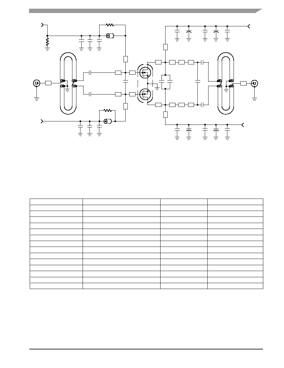
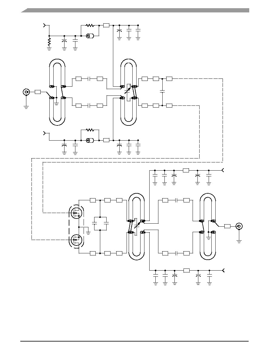
Figure 1. 820-900 MHz Narrowband Test Circuit Schematic
Z10, Z11
1.054 x 0.150 Microstrip
Z12, Z13
0.225 x 0.507 Microstrip
Z14, Z15
0.440 x 0.335 Microstrip
Z16, Z17
0.123 x 0.140 Microstrip
PCB
Arlon GX-0300-55-22, 0.030,
r
= 2.5
Z1, Z18
0.401 x 0.810 Microstrip
Z2, Z3
0.563 x 0.810 Microstrip
Z4, Z5
1.643 x 0.058 Microstrip
Z6, Z7
0.416 x 0.727 Microstrip
Z8, Z9
0.191 x 0.507 Microstrip
RF
INPUT
C2
R3
C1
C3
V
BIAS
Z6
C4
Z7
C5
Z1
DUT
C8
C9
R2
B2
V
SUPPLY
Z8
Z9
Z13
Z15
Z17
C13
C24
C19
V
SUPPLY
RF
OUTPUT
Z18
V
BIAS
Z4
Z5
Z2
Z3
Z11
Z10
+
+
+
C7
R1
B1
C14
C12
Z12
Z14
Z16
C20
C22
+
C21
C23
C15
+
C16
C18
+
C17
C10 C11
C6
COAX1
COAX2
COAX3
COAX4
Table 5. 820-900 MHz Narrowband Test Circuit Component Designations and Values
Part
Description
Part Number
Manufacturer
B1, B2
Ferrite Beads, Short
2743019447
Fair-Rite
C1, C9
1.0 µF, 50 V Tantulum Chip Capacitors
T491C105K050AS
Kemet
C2, C7, C17, C21
0.1 µF, 50 V Chip Capacitors
CDR33BX104AKWS
Kemet
C3, C8, C16, C20
1000 pF 100B Chip Capacitors
100B102JP50X
ATC
C4, C5, C13, C14
100 pF 100B Chip Capacitors
100B101JP500X
ATC
C6, C12
8.2 pF 600B Chip Capacitors
600B8R2BT250XT
ATC
C10
9.1 pF 600B Chip Capacitor
600B9R1BT250XT
ATC
C11
1.8 pF 600B Chip Capacitor
600B1R8BT250XT
ATC
C15, C19
47 µF, 50 V Electrolytic Capacitors
MVK50VC47RM8X10TP
Nippon
C18, C22
470 µF, 63 V Electrolytic Capacitors
SME63V471M12X25LL
United Chemi-Con
C23, C24
22 pF 600B Chip Capacitors
600B220FT250XT
ATC
Coax1, 2, 3, 4
50 , Semi Rigid Coax, 2.06 Long
UT-141A-TP
Micro-Coax
R1, R2
10 , 1/8 W Chip Resistors (1206)
CRCW1206100J
Dale/Vishay
R3
1 k, 1/8 W Chip Resistor (1206)
CRCW1206102J
Dale/Vishay

4
RF Device Data
Freescale Semiconductor
MRF6P3300HR3 MRF6P3300HR5
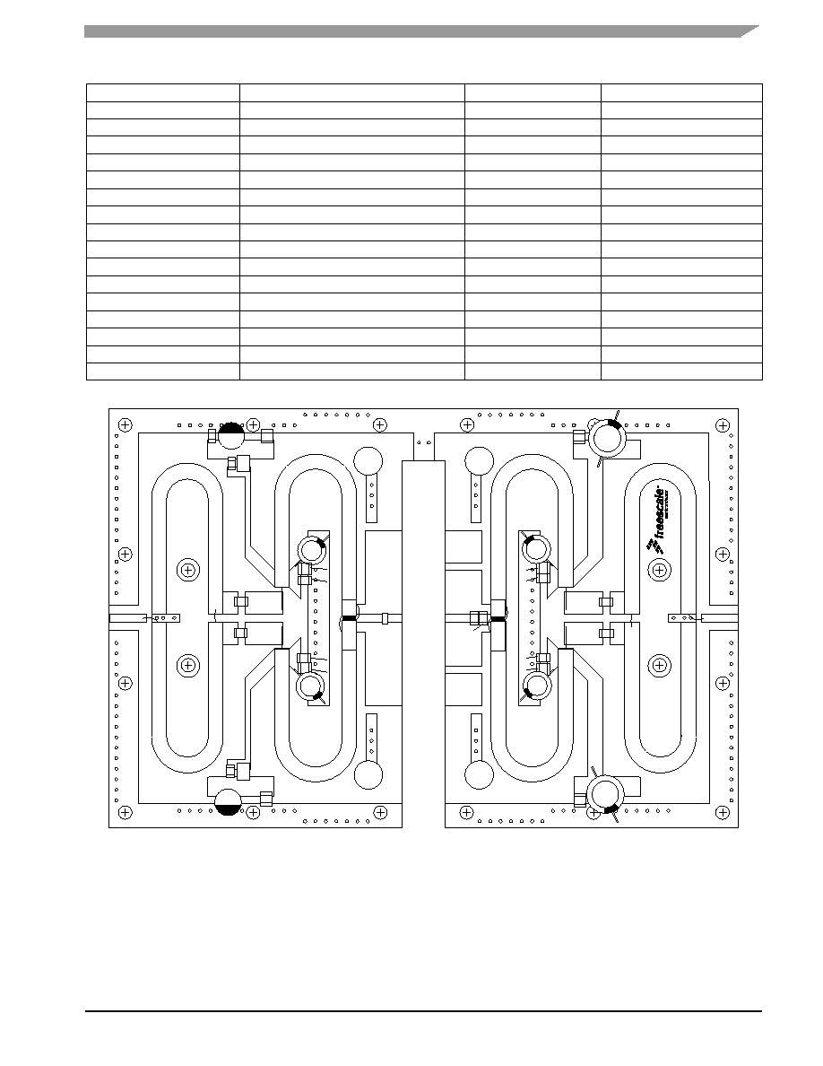
Figure 2. 820-900 MHz Narrowband Test Circuit Component Layout
CUT
OUT
AREA
C1
B1
R1
R3
C2 C3
C4
C5
C6
C9
C7
C8
B2
R2
C19
C24
C20
C21
C22
C10
C11
C12
C13
C14
C23
C15
C16
C17
C18
MRF6P9220, Rev
.
2
COAX3
COAX4
COAX1
COAX2
V
GG
V
GG
V
DD
V
DD
MRF6P3300HR3 MRF6P3300HR5
5
RF Device Data
Freescale Semiconductor
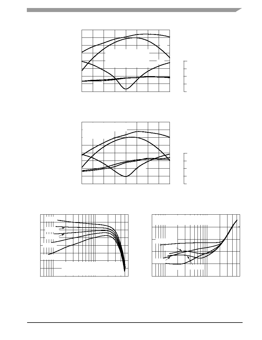
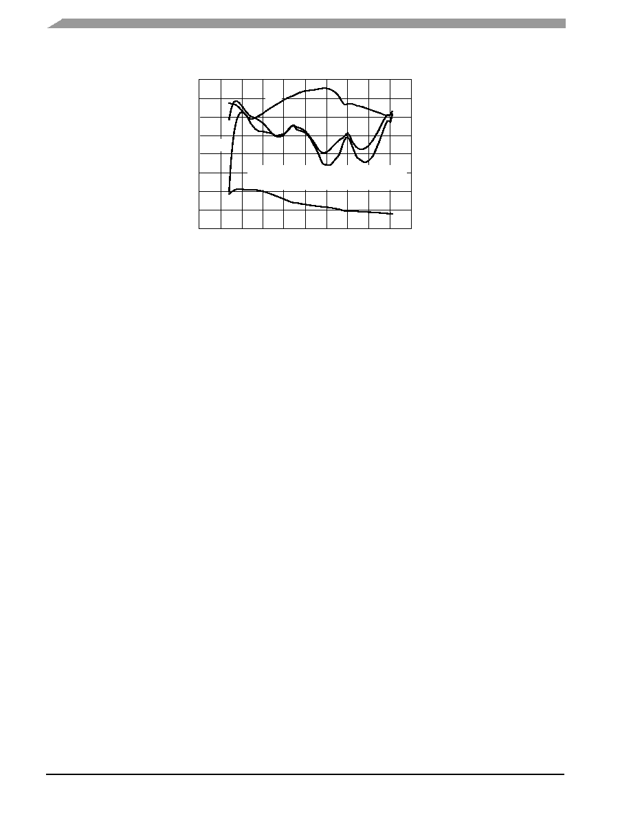
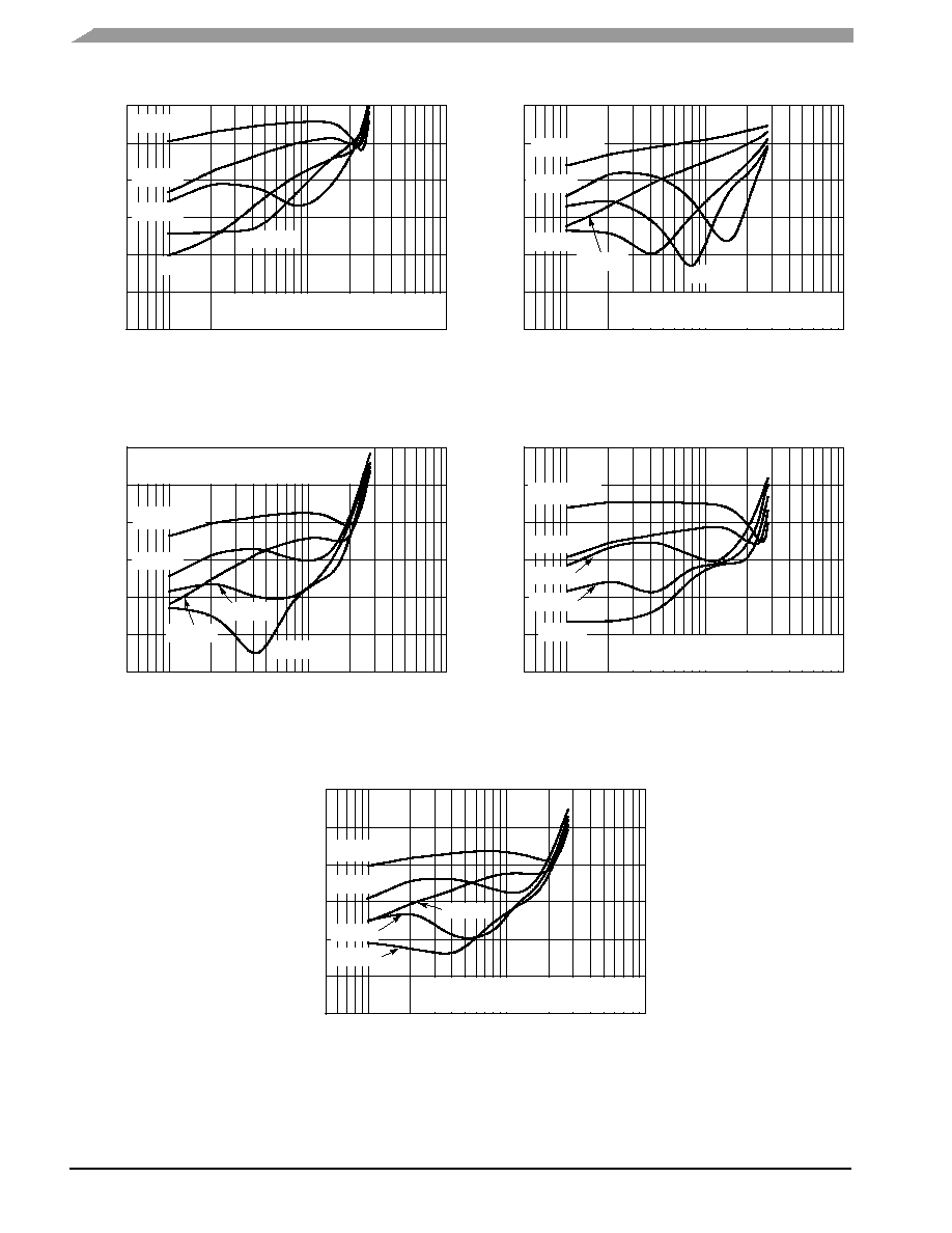
TYPICAL NARROWBAND CHARACTERISTICS
G
ps
, POWER GAIN (dB)
IRL, INPUT RETURN LOSS (dB)
ACPR (dBc)
-25
-10
-20
900
820
IRL
G
ps
ACPR
f, FREQUENCY (MHz)
Figure 3. Single-Carrier OFDM Broadband Performance @ 60 Watts Avg.
890
880
870
860
850
840
830
21
20
-65
31
27
-50
-55
-60
D
, DRAIN
EFFICIENCY (%)
D
18.5
18
17.5
17
20.5
19.5
19
29
25
-45
-5
-15
V
DD
= 32 Vdc, P
out
= 60 W (Avg.)
I
DQ
= 1600 mA, 8K Mode OFDM
64 QAM Data Carrier Modulation
5 Symbols
G
ps
, POWER GAIN (dB)
IRL, INPUT RETURN LOSS (dB)
ACPR (dBc)
-25
-10
-20
900
820
IRL
G
ps
ACPR
f, FREQUENCY (MHz)
Figure 4. Single-Carrier OFDM Broadband Performance @ 120 Watts Avg.
890
880
870
860
850
840
830
21
20
-53
44
40
-47
-49
-51
D
, DRAIN
EFFICIENCY (%)
D
18.5
18
17.5
17
20.5
19.5
19
42
38
-45
-5
-15
Figure 5. Two-Tone Power Gain versus
Output Power
17.5
21.5
5
I
DQ
= 800 mA
2000 mA
P
out
, OUTPUT POWER (WATTS) PEP
21
20
19
100
600
G
ps
, POWER GAIN (dB)
18
1600 mA
20.5
19.5
18.5
10
1200 mA
2400 mA
V
DD
= 32 Vdc
f1 = 857 MHz, f2 = 863 MHz
Two-Tone Measurements, 6 MHz Tone Spacing
Figure 6. Third Order Intermodulation Distortion
versus Output Power
P
out
, OUTPUT POWER (WATTS) PEP
100
-20
-30
-40
-50
-60
10
INTERMODULA
TION DIST
ORTION
(dBc)
IMD, THIRD ORDER
-10
I
DQ
= 2400 mA
800 mA
2000 mA
1200 mA
1600 mA
V
DD
= 32 Vdc, f1 = 857 MHz, f2 = 863 MHz
Two-Tone Measurements, 6 MHz Tone Spacing
600
V
DD
= 32 Vdc, P
out
= 120 W (Avg.)
I
DQ
= 1600 mA, 8K Mode OFDM
64 QAM Data Carrier
Modulation, 5 Symbols
5
6
RF Device Data
Freescale Semiconductor
MRF6P3300HR3 MRF6P3300HR5
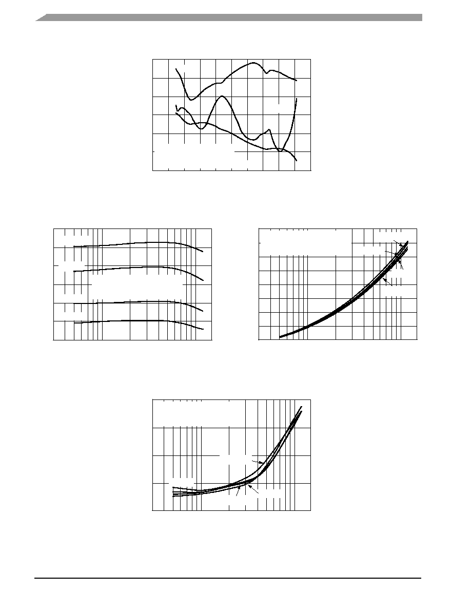
TYPICAL NARROWBAND CHARACTERISTICS
Figure 7. Intermodulation Distortion Products
versus Output Power
-70
-10
10
7th Order
P
out
, OUTPUT POWER (WATTS) PEP
V
DD
= 32 Vdc, I
DQ
= 1600 mA, f1 = 857 MHz
f2 = 863 MHz, Two-Tone Measurements
3rd Order
-20
-30
-40
-50
100
600
IMD, INTERMODULA
TION
DIST
ORTION
(dBc)
-60
5th Order
5
Figure 8. Intermodulation Distortion Products
versus Tone Spacing @ 860 MHz
10
-55
-20
0.01
7th Order
TWO-TONE SPACING (MHz)
V
DD
= 32 Vdc, P
out
= 270 W (PEP), I
DQ
= 1600 mA
Two-Tone Measurements, f = 860 MHz
5th Order
3rd Order
-25
-30
-40
-50
1
40
IMD, INTERMODULA
TION
DIST
ORTION
(dBc)
0.1
-35
-45
Figure 9. Pulse CW Output Power versus
Input Power
44
64
34
P
in
, INPUT POWER (dBm)
V
DD
= 32 Vdc, I
DQ
= 1600 mA
Pulsed CW, 8
µsec(on), 1 msec(off)
f = 860 MHz
61
59
57
52
36
38
40
42
Actual
Ideal
63
53
32
P
out
, OUTPUT POWER (dBm) 55
60
58
56
54
33
35
37
39
41
43
62
P1dB = 55.20 dBm
(330.94 W)
P3dB = 55.87 dBm
(386.48 W)
P6dB = 56.28 dBm
(424.54 W)
ACPR, ADJACENT CHANNEL POWER RA
TIO
(dBc)
Figure 10. Single-Carrier DVBT OFDM ACPR,
Power Gain and Drain Efficiency
versus Output Power
15
-64
P
out
, OUTPUT POWER (WATTS) AVG.
45
-40
30
20
-44
-48
-60
30
40
100
-56
D
, DRAIN EFFICIENCY (%), G
ps
, POWER GAIN (dB)
G
ps
ACPR
V
DD
= 32 Vdc, I
DQ
= 1600 mA, f = 860 MHz
8K Mode OFDM, 64 QAM Data Carrier
Modulation, 5 Symbols
90
-30
_C
40
50
60 70 80
25
_C
20
200
35
25
-52
-30
_C
25
_C
85
_C
T
C
= 85
_C
25
_C
D
MRF6P3300HR3 MRF6P3300HR5
7
RF Device Data
Freescale Semiconductor
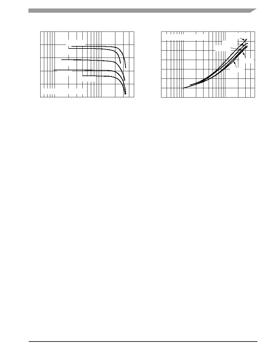
TYPICAL NARROWBAND CHARACTERISTICS
800
16
23
0
70
P
out
, OUTPUT POWER (WATTS) CW
Figure 11. Power Gain and Drain Efficiency
versus CW Output Power
V
DD
= 32 Vdc
I
DQ
= 1600 mA
f = 860 MHz
100
10
21
20
19
18
17
50
40
30
20
10
D
,
DRAIN
EFFICIENCY (%)
G
ps
D
G
ps
, POWER GAIN (dB)
5
T
C
= -30
_C
85
_C
25
_C
-30
_C
22
60
25
_C
85
_C
Figure 12. Power Gain versus Output Power
P
out
, OUTPUT POWER (WATTS) CW
V
DD
= 12 V
G
ps
, POWER GAIN (dB)
400
16.5
21.5
50
20.5
17.5
200
18
18.5
24 V
I
DQ
= 1600 mA
f = 860 MHz
20 V
16 V
32 V
0
19.5
100
150
250
300
350
28 V
17
19
20
21
210
10
10
90
T
J
, JUNCTION TEMPERATURE (
∞C)
Figure 13. MTTF Factor versus Junction Temperature
This above graph displays calculated MTTF in hours x ampere
2
drain current. Life tests at elevated temperatures have correlated to
better than
±10% of the theoretical prediction for metal failure. Divide
MTTF factor by I
D
2
for MTTF in a particular application.
10
8
10
7
120
140
160
180
200
MTTF
F
ACT
OR (HOURS x AMPS
2
)
10
9
100
190
170
150
130
110
8
RF Device Data
Freescale Semiconductor
MRF6P3300HR3 MRF6P3300HR5
DIGITAL TEST SIGNALS
12
0.0001
100
0
PEAK-TO-AVERAGE (dB)
Figure 14. Single-Carrier DVTB OFDM
10
1
0.1
0.01
0.001
2
4
6
8
PROBABILITY
(%)
8K Mode DVTB OFDM
64 QAM Data Carrier Modulation
5 Symbols
5
-20
-5
7.61 MHz
f, FREQUENCY (MHz)
Figure 15. 8K Mode DVBT OFDM Spectrum
-30
-40
-50
-90
-70
-80
-100
-110
-60
-4
-3
-2
-1
0
1
2
3
4
20 kHz BW
(dB)
20 kHz BW
10
ACPR Measured at 3.9 MHz Offset
from Center Frequency
IMRU
4.0
-100
-10
0
IMRL
f, FREQUENCY (MHz)
Reference
Point
-20
-30
-40
-50
-60
-70
-80
-90
0.8
-0.8
1.6
2.4
3.2
-4.0 -3.2
-2.4 -1.6
3.25 MHz
Offset
3.25 MHz
Offset
(dB)
0.0001
100
0
PEAK-TO-AVERAGE (dB)
Figure 16. Single-Carrier ATSC 8VSB
10
1
0.1
0.01
0.001
2
4
6
8
PROBABILITY
(%)
ATSC 8VSB
1
3
5
7
Figure 17. ATSC 8VSB Spectrum
MRF6P3300HR3 MRF6P3300HR5
9
RF Device Data
Freescale Semiconductor
f
MHz
Z
source
Z
load
830
845
860
4.52 - j6.73
3.89 - j5.81
4.22 - j6.38
4.89 - j1.35
5.06 - j1.01
5.18 - j0.58
V
DD
= 32 Vdc, I
DQ
= 1600 mA, P
out
= 270 W PEP
Z
source
= Test circuit impedance as measured from
gate to gate, balanced configuration.
Z
load
= Test circuit impedance as measured
from drain to drain, balanced configuration.
Z source
Z load
Input
Matching
Network
Device
Under
Test
Output
Matching
Network
-
-
+
+
Figure 18. 820-900 MHz Narrowband Series Equivalent Source and Load Impedance
Z
o
= 10
f = 890 MHz
f = 830 MHz
Z
load
Z
source
875
890
3.39 - j4.32
3.54 - j5.10
5.27 - j0.11
5.36 + j0.43
f = 830 MHz
f = 890 MHz
10
RF Device Data
Freescale Semiconductor
MRF6P3300HR3 MRF6P3300HR5
Figure 19. 470-860 MHz Broadband Test Circuit Schematic
RF
INPUT
R1
C26
V
BIAS
C1
Z1
RF
OUTPUT
Z2
R2
B1
COAX1
COAX2
C28
+
Z3
C2
Z4
Z5
COAX3
COAX4
C9
Z8
Z9
Z10
Z11
C10
Z12
Z13
C3
+
C5
C7
Z6
C27
V
BIAS
R3
B2
C29
+
C4
+
C6
C8
Z7
C18
C20
Z26
Z24
COAX7
COAX8
C14
+
Z25
C21
Z22
Z23
COAX5
COAX6
C13
Z18
Z19
Z16
Z17
C11
Z14
Z15
DUT
Z20
C12
C16
C22
+
C24
V
SUPPLY
C19
C15
+
Z21
C17
C23
+
C25
V
SUPPLY
Z14, Z15
0.276 x 0.420 Microstrip
Z16, Z17
0.072 x 0.420 Microstrip
Z18, Z19
0.072 x 0.031 Microstrip
Z20, Z21
1.404 x 0.141 Microstrip
Z22, Z23
0.363 x 0.214 Microstrip
Z24, Z25
0.139 x 0.214 Microstrip
PCB
Arlon GX-0300-55-22, 0.030,
r
= 2.5
Z1, Z26
0.351 x 0.081 Microstrip
Z2, Z3
0.139 x 0.214 Microstrip
Z4, Z5
0.364 x 0.214 Microstrip
Z6, Z7
1.154 x 0.051 Microstrip
Z8, Z9
0.086 x 0.100 Microstrip
Z10, Z11
0.184 x 0.802 Microstrip
Z12, Z13
0.164 x 0.802 Microstrip
MRF6P3300HR3 MRF6P3300HR5
11
RF Device Data
Freescale Semiconductor
Table 6. 470-860 MHz Broadband Test Circuit Component Designations and Values
Part
Description
Part Number
Manufacturer
B1, B2
Ferrite Beads, Short
2743019447
Fair-Rite
C1, C2, C20, C21
43 pF 600B Chip Capacitors
700B430FW500XT
ATC
C3, C4, C14, C15
100 µF, 50 V Electrolytic Capacitors
515D107M050BB6A
Vishay
C5, C6, C16, C17
220 nF, 100 V Chip Capacitors
C1812C224K5RAC
Kemet
C7, C8, C18, C19
0.01 µF, 100 V Chip Capacitors
C1210C103J1RAC
Kemet
C9, C13
0.8-8.0 pF Variable Capacitors, Gigatrim
27291SL
Johanson
C10
15 pF 600B Chip Capacitor
600S150FT250XT
ATC
C11
16 pF 600B Chip Capacitor
600B160FT250XT
ATC
C12
4.3 pF 600B Chip Capacitor
600B4R3BT250XT
ATC
C22, C23
470 µF, 63 V Electrolytic Capacitors
NACZF471M63V
Nippon
C24, C25, C26, C27
0.1 µF, 50 V Chip Capacitors
CDR33BX104AKWS
Kemet
C28, C29
10 µF, 50 V Electrolytic Capacitors
ECE-V1HA100SP
Panasonic
Coax1, 2, 7, 8
50 , Semi Rigid Coax, 3.00 Long
UT-141C-50-SP
Micro-Coax
Coax3, 4, 5, 6
25 , Semi Rigid Coax, 3.00 Long
UT-141C-25
Micro-Coax
R1
1 k, 1/8 W Resistor (1206)
CRCW1206102J
Dale/Vishay
R2, R3
10 , 1/8 W Resistors (1206)
CRCW1206100J
Dale/Vishay
Figure 20. 470-860 MHz Broadband Test Circuit Component Layout
R1
MRF6P93300
C28
C26
COAX1
Rev
. 3
C3
C5
C7
C9
C10
C1
C2
C4
C8
C6
C27
C29
R3
B2
V
GG
V
GG
V
DD
C22
COAX5
C24
C14
C19
C18
C12
C11
C13
C20
C21
C15
V
DD
C25
C23
CUT
OUT
AREA
COAX2
COAX3
COAX4
R2
B1
COAX7
COAX8
COAX6
C18
C16
C17
12
RF Device Data
Freescale Semiconductor
MRF6P3300HR3 MRF6P3300HR5
TYPICAL TWO-TONE BROADBAND CHARACTERISTICS
IMD,
INTERMODULA
TION
DIST
ORTION
(dBc)
Figure 21. Two-Tone Broadband Performance @ P
out
= 270 Watts PEP
16
-48
f, FREQUENCY (MHz)
48
-24
36
24
-27
-33
-45
400
-42
D
, DRAIN EFFICIENCY (%), G
ps
, POWER GAIN (dB)
G
ps
IMD
44
900
40
32
-39
D
500
600
700
800
V
DD
= 32 Vdc, P
out
= 270 W (PEP), I
DQ
= 1600 mA
Two-Tone Measurements, 6 MHz Tone Spacing
28
20
-30
-36
MRF6P3300HR3 MRF6P3300HR5
13
RF Device Data
Freescale Semiconductor
TYPICAL TWO-TONE BROADBAND CHARACTERISTICS
Figure 22. Two-Tone Power Gain versus
Output Power @ 473 MHz
21
24.5
5
I
DQ
= 2400 mA
2000 mA
P
out
, OUTPUT POWER (WATTS) PEP
24
23
22
100
1000
G
ps
, POWER GAIN (dB)
1600 mA
23.5
22.5
21.5
10
1200 mA
800 mA
Figure 23. Two-Tone Power Gain versus
Output Power @ 560 MHz
20
23.5
5
I
DQ
= 2400 mA
2000 mA
P
out
, OUTPUT POWER (WATTS) PEP
23
22
21
100
1000
G
ps
, POWER GAIN (dB)
1600 mA
22.5
21.5
20.5
10
1200 mA
800 mA
Figure 24. Two-Tone Power Gain versus
Output Power @ 660 MHz
18.5
21
5
I
DQ
= 2400 mA
2000 mA
P
out
, OUTPUT POWER (WATTS) PEP
20.5
19
100
1000
G
ps
, POWER GAIN (dB)
1600 mA
20
19.5
10
1200 mA
800 mA
Figure 25. Two-Tone Power Gain versus
Output Power @ 760 MHz
16.5
19
5
I
DQ
= 2400 mA
2000 mA
P
out
, OUTPUT POWER (WATTS) PEP
18.5
17
100
1000
G
ps
, POWER GAIN (dB)
1600 mA
18
17.5
10
1200 mA
800 mA
V
DD
= 32 Vdc, f1 = 757 MHz, f2 = 763 MHz
Two-Tone Measurements, 6 MHz Tone Spacing
V
DD
= 32 Vdc, f1 = 657 MHz, f2 = 663 MHz
Two-Tone Measurements, 6 MHz Tone Spacing
Figure 26. Two-Tone Power Gain versus
Output Power @ 857 MHz
17.5
20
5
I
DQ
= 2400 mA
2000 mA
P
out
, OUTPUT POWER (WATTS) PEP
19.5
18
100
1000
G
ps
, POWER GAIN (dB)
1600 mA
19
18.5
10
1200 mA
800 mA
V
DD
= 32 Vdc, f1 = 854 MHz, f2 = 860 MHz
Two-Tone Measurements, 6 MHz Tone Spacing
V
DD
= 32 Vdc, f1 = 470 MHz, f2 = 476 MHz
Two-Tone Measurements, 6 MHz Tone Spacing
V
DD
= 32 Vdc, f1 = 557 MHz, f2 = 563 MHz
Two-Tone Measurements, 6 MHz Tone Spacing
14
RF Device Data
Freescale Semiconductor
MRF6P3300HR3 MRF6P3300HR5
TYPICAL TWO-TONE BROADBAND CHARACTERISTICS
Figure 27. Third Order Intermodulation
Distortion versus Output Power @ 473 MHz
P
out
, OUTPUT POWER (WATTS) PEP
100
-30
-35
-40
-50
-55
10
INTERMODULA
TION DIST
ORTION
(dBc)
IMD, THIRD ORDER
-25
I
DQ
= 800 mA
2000 mA
1200 mA
1600 mA
1000
-45
2400 mA
Figure 28. Third Order Intermodulation
Distortion versus Output Power @ 560 MHz
P
out
, OUTPUT POWER (WATTS) PEP
100
-30
-35
-40
-50
-55
10
INTERMODULA
TION DIST
ORTION
(dBc)
IMD, THIRD ORDER
-25
I
DQ
= 800 mA
2000 mA
1200 mA
1600 mA
V
DD
= 32 Vdc, f1 = 557 MHz, f2 = 563 MHz
Two-Tone Measurements, 6 MHz Tone Spacing
1000
-45
2400 mA
Figure 29. Third Order Intermodulation
Distortion versus Output Power @ 660 MHz
P
out
, OUTPUT POWER (WATTS) PEP
100
-30
-35
-40
-50
-55
10
INTERMODULA
TION DIST
ORTION
(dBc)
IMD, THIRD ORDER
-25
I
DQ
= 800 mA
2000 mA
1200 mA
1600 mA
V
DD
= 32 Vdc, f1 = 657 MHz, f2 = 663 MHz
Two-Tone Measurements, 6 MHz Tone Spacing
1000
-45
2400 mA
Figure 30. Third Order Intermodulation
Distortion versus Output Power @ 760 MHz
P
out
, OUTPUT POWER (WATTS) PEP
100
-30
-35
-40
-50
-55
10
INTERMODULA
TION DIST
ORTION
(dBc)
IMD, THIRD ORDER
-25
I
DQ
= 800 mA
2000 mA
1200 mA
1600 mA
V
DD
= 32 Vdc, f1 = 757 MHz, f2 = 763 MHz
Two-Tone Measurements, 6 MHz Tone Spacing
1000
-45
2400 mA
V
DD
= 32 Vdc, f1 = 470 MHz, f2 = 476 MHz
Two-Tone Measurements, 6 MHz Tone Spacing
Figure 31. Third Order Intermodulation
Distortion versus Output Power @ 857 MHz
P
out
, OUTPUT POWER (WATTS) PEP
100
-30
-35
-40
-50
-55
10
INTERMODULA
TION DIST
ORTION
(dBc)
IMD, THIRD ORDER
-25
I
DQ
= 800 mA
2000 mA
1200 mA
1600 mA
V
DD
= 32 Vdc, f1 = 854 MHz, f2 = 860 MHz
Two-Tone Measurements, 6 MHz Tone Spacing
1000
-45
2400 mA

MRF6P3300HR3 MRF6P3300HR5
15
RF Device Data
Freescale Semiconductor
TYPICAL TWO-TONE BROADBAND CHARACTERISTICS
Figure 32. Intermodulation Distortion
Products versus Tone Spacing @ 470 MHz
10
-60
0
0.1
7th Order
TWO-TONE SPACING (MHz)
V
DD
= 32 Vdc, P
out
= 270 W (PEP), I
DQ
= 1600 mA
Two-Tone Measurements
f1 = 470 MHz, f2 = 470 MHz + Tone Spacing
5th Order
3rd Order
-10
-20
-40
-50
1
100
IMD, INTERMODULA
TION
DIST
ORTION
(dBc)
-30
Figure 33. Intermodulation Distortion
Products versus Tone Spacing @ 560 MHz
10
-60
0
0.01
7th Order
TWO-TONE SPACING (MHz)
V
DD
= 32 Vdc, P
out
= 270 W (PEP), I
DQ
= 1600 mA
Two-Tone Measurements, f = 560 MHz
5th Order
3rd Order
-10
-20
-40
-50
1
100
IMD, INTERMODULA
TION
DIST
ORTION
(dBc)
-30
0.1
Figure 34. Intermodulation Distortion
Products versus Tone Spacing @ 660 MHz
10
-60
0
0.01
7th Order
TWO-TONE SPACING (MHz)
V
DD
= 32 Vdc, P
out
= 270 W (PEP), I
DQ
= 1600 mA
Two-Tone Measurements, f = 660 MHz
5th Order
3rd Order
-10
-20
-40
-50
1
100
IMD, INTERMODULA
TION
DIST
ORTION
(dBc)
-30
0.1
Figure 35. Intermodulation Distortion
Products versus Tone Spacing @ 760 MHz
10
-60
0
0.01
7th Order
TWO-TONE SPACING (MHz)
V
DD
= 32 Vdc, P
out
= 270 W (PEP), I
DQ
= 1600 mA
Two-Tone Measurements, f = 760 MHz
5th Order
3rd Order
-10
-20
-40
-50
1
100
IMD, INTERMODULA
TION
DIST
ORTION
(dBc)
-30
0.1
Figure 36. Intermodulation Distortion
Products versus Tone Spacing @ 860 MHz
10
-60
0
0.1
7th Order
TWO-TONE SPACING (MHz)
V
DD
= 32 Vdc, P
out
= 270 W (PEP), I
DQ
= 1600 mA
Two-Tone Measurements, 6 MHz Tone Spacing
f1 = 860 MHz - Tone Spacing, f2 = 860 MHz
5th Order
3rd Order
-10
-20
-40
-50
1
100
IMD, INTERMODULA
TION
DIST
ORTION
(dBc)
-30
16
RF Device Data
Freescale Semiconductor
MRF6P3300HR3 MRF6P3300HR5
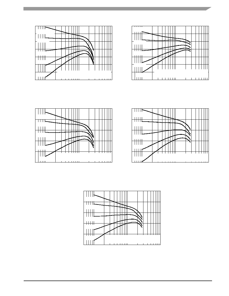
TYPICAL DVBT OFDM BROADBAND CHARACTERISTICS
ACPR,
ADJACENT CHANNEL POWER RA
TIO
(dBc)
Figure 37. Single-Carrier OFDM Broadband
Performance @ 60 Watts Avg.
18
-58
f, FREQUENCY (MHz)
30
-52
24
20
-53
-54
-57
400
-56
D
, DRAIN EFFICIENCY (%), G
ps
, POWER GAIN (dB)
G
ps
ACPR
28
900
26
22
-55
D
500
600
700
800
Figure 38. Single-Carrier DVBT OFDM Power
Gain versus Output Power
18
24
3
f = 560 MHz
P
out
, OUTPUT POWER (WATTS) AVG.
23
21
20
100
200
G
ps
, POWER GAIN (dB)
22
19
10
660 MHz
V
DD
= 32 Vdc, I
DQ
= 1600 mA
8K Mode OFDM, 64 QAM Data Carrier
Modulation, 5 Symbols
760 MHz
860 MHz
D
,
DRAIN
EFFICIENCY (%)
Figure 39. Single-Carrier DVBT OFDM Drain
Efficiency versus Output Power
5
45
3
P
out
, OUTPUT POWER (WATTS) AVG.
40
30
25
100
200
35
20
10
V
DD
= 32 Vdc, I
DQ
= 1600 mA
8K Mode OFDM, 64 QAM Data Carrier
Modulation, 5 Symbols
15
10
f = 660 MHz
560 MHz
760 MHz
860 MHz
ACPR, ADJACENT CHANNEL POWER RA
TIO
(dBc)
Figure 40. Single-Carrier DVBT OFDM ACPR
versus Output Power
-65
-45
3
P
out
, OUTPUT POWER (WATTS) AVG.
-50
100
200
-55
10
V
DD
= 32 Vdc, I
DQ
= 1600 mA
8K Mode OFDM, 64 QAM Data Carrier
Modulation, 5 Symbols
-60
f = 860 MHz
560 MHz
760 MHz
660 MHz
V
DD
= 32 Vdc, P
out
= 60 W (Avg.)
I
DQ
= 1600 mA, 8K Mode OFDM
64 QAM Data Carrier Modulation, 5 Symbols
MRF6P3300HR3 MRF6P3300HR5
17
RF Device Data
Freescale Semiconductor
TYPICAL CW BROADBAND CHARACTERISTICS
Figure 41. CW Power Gain versus
Output Power
16
26
5
f = 560 MHz
P
out
, OUTPUT POWER (WATTS) CW
24
20
100
500
G
ps
, POWER GAIN (dB)
22
18
10
660 MHz
V
DD
= 32 Vdc, I
DQ
= 1600 mA
760 MHz
860 MHz
470 MHz
D
,
DRAIN
EFFICIENCY (%)
Figure 42. CW Drain Efficiency versus
Output Power
0
70
3
P
out
, OUTPUT POWER (WATTS) CW
60
40
30
100
500
50
20
10
V
DD
= 32 Vdc, I
DQ
= 1600 mA
10
f = 660 MHz
560 MHz
760 MHz
860 MHz
470 MHz
18
RF Device Data
Freescale Semiconductor
MRF6P3300HR3 MRF6P3300HR5
TYPICAL CW BROADBAND CHARACTERISTICS
Figure 43. Pulse CW Output Power versus
Input Power @ 470 MHz
33
57
29
P
in
, INPUT POWER (dBm)
V
DD
= 32 Vdc, I
DQ
= 1600 mA
Pulsed CW, 8
µsec(on), 1 msec(off)
f = 470 MHz
51
30
31
32
Actual
Ideal
56.5
28
P
out
, OUTPUT POWER (dBm)
55
54
53
52
28.5
P1dB = 53.59 dBm
(228.67 W)
56
55.5
54.5
53.5
52.5
51.5
29.5
30.5
31.5
32.5
Figure 44. Pulse CW Output Power versus
Input Power @ 560 MHz
36
59
30
P
in
, INPUT POWER (dBm)
V
DD
= 32 Vdc, I
DQ
= 1600 mA
Pulsed CW, 8
µsec(on), 1 msec(off)
f = 560 MHz
53
31
32
34
Actual
Ideal
29
P
out
, OUTPUT POWER (dBm)
58
57
55
54
P1dB = 54.84 dBm
(304.81 W)
33
35
56
P3dB = 55.49 dBm
(353.76 W)
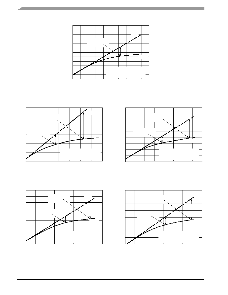
Figure 45. Pulse CW Output Power versus
Input Power @ 660 MHz
38
60
P
in
, INPUT POWER (dBm)
V
DD
= 32 Vdc, I
DQ
= 1600 mA
Pulsed CW, 8
µsec(on), 1 msec(off)
f = 660 MHz
51
31
32
34
Actual
Ideal
30
P
out
, OUTPUT POWER (dBm)
58
57
55
54
P1dB = 54.04 dBm
(253.67 W)
33
35
56
P3dB = 54.88 dBm
(307.45 W)
59
53
52
36
37
Figure 46. Pulse CW Output Power versus
Input Power @ 760 MHz
39
60
P
in
, INPUT POWER (dBm)
V
DD
= 32 Vdc, I
DQ
= 1600 mA
Pulsed CW, 8
µsec(on), 1 msec(off)
f = 760 MHz
51
32
33
35
Actual
Ideal
31
P
out
, OUTPUT POWER (dBm)
58
57
55
54
P1dB = 54.56 dBm
(286.06 W)
34
36
56
P3dB = 55.25 dBm
(334.73 W)
59
53
52
37
38
Figure 47. Pulse CW Output Power versus
Input Power @ 860 MHz
40
60
P
in
, INPUT POWER (dBm)
V
DD
= 32 Vdc, I
DQ
= 1600 mA
Pulsed CW, 8
µsec(on), 1 msec(off)
f = 860 MHz
52
33
34
36
Actual
Ideal
32
P
out
, OUTPUT POWER (dBm)
58
57
55
54
P1dB = 54.82 dBm
(303.25 W)
35
37
56
P3dB = 55.58 dBm
(361.21 W)
59
53
38
39
MRF6P3300HR3 MRF6P3300HR5
19
RF Device Data
Freescale Semiconductor
TYPICAL ATSC 8VSB BROADBAND CHARACTERISTICS
ACPR,
ADJACENT CHANNEL POWER RA
TIO
(dBc)
Figure 48. Single-Carrier ATSC 8VSB
Broadband Performance @ 100 Watts Avg.
15
-33
f, FREQUENCY (MHz)
40
-23
30
20
-24
-25
-32
400
-27
D
, DRAIN EFFICIENCY (%), G
ps
, POWER GAIN (dB)
G
ps
ACPR
V
DD
= 32 Vdc, P
out
= 100 W (Avg.)
I
DQ
= 1700 mA, ATSC 8VSB
37.5
900
35
25
-26
D
500
600
700
800
Figure 49. Single-Carrier ATSC 8VSB Power
Gain versus Output Power
17
24
3
f = 560 MHz
P
out
, OUTPUT POWER (WATTS) AVG.
23
21
20
100
200
G
ps
, POWER GAIN (dB)
22
19
10
660 MHz
V
DD
= 32 Vdc, I
DQ
= 1700 mA
760 MHz
860 MHz
D
,
DRAIN
EFFICIENCY (%)
Figure 50. Single-Carrier ATSC 8VSB Drain
Efficiency versus Output Power
0
50
3
P
out
, OUTPUT POWER (WATTS) AVG.
40
30
100
200
20
10
V
DD
= 32 Vdc, I
DQ
= 1700 mA
ATSC 8VSB
10
f = 660 MHz
560 MHz
760 MHz
860 MHz
ACPR, ADJACENT CHANNEL POWER RA
TIO
(dBc)
Figure 51. Single-Carrier ATSC 8VSB ACPR
versus Output Power
-40
-15
3
P
out
, OUTPUT POWER (WATTS) AVG.
-20
100
200
-25
10
V
DD
= 32 Vdc, I
DQ
= 1700 mA
ATSC 8VSB
-35
f = 860 MHz
760 MHz
660 MHz
32.5
27.5
22.5
17.5
-28
-29
-30
-31
470 MHz
18
470 MHz
-30
470 MHz
560 MHz
20
RF Device Data
Freescale Semiconductor
MRF6P3300HR3 MRF6P3300HR5
TYPICAL PAL B/G BROADBAND CHARACTERISTICS
PEAK
SYNC (W)
Figure 52. Peak Sync, Power Gain and Drain
Efficiency versus Frequency
15
245
f, FREQUENCY (MHz)
50
280
40
20
275
270
400
D
, DRAIN EFFICIENCY (%), G
ps
, POWER GAIN (dB)
G
ps
V
DD
= 32 Vdc, I
DQ
= 1500 mA
Sync Compression
Input = 33%, Output = 27%
900
45
30
265
D
500
600
700
800
35
25
260
255
250
Peak Sync
MRF6P3300HR3 MRF6P3300HR5
21
RF Device Data
Freescale Semiconductor
Figure 53. 470-860 MHz Broadband Series Equivalent Source and Load Impedance
f = 470 MHz
f = 860 MHz
Z
load
Z
o
= 25
Z
source
f = 470 MHz
f = 860 MHz
Z
o
= 25
8.86 - j2.87
560
f
MHz
Z
source
Z
load
470
510
8.77 - j5.43
8.74 - j4.17
6.09 - j4.37
6.39 - j1.65
6.69 - j2.45
V
DD
= 32 Vdc, I
DQ
= 1600 mA, P
out
= 270 W PEP
Z
source
= Test circuit impedance as measured from
gate to gate, balanced configuration.
Z
load
= Test circuit impedance as measured
from drain to drain, balanced configuration.
Z source
Z load
Input
Matching
Network
Device
Under
Test
Output
Matching
Network
-
-
+
+
610
660
12.41 - j3.53
10.55 - j2.45
7.36 - j1.95
7.73 - j1.75
6.81 - j10.41
710
760
13.11 - j6.04
11.29 - j10.15
7.95 - j1.20
8.18 - j1.36
7.81 - j1.60
860
3.73 - j9.66
6.94 - j2.49
810

22
RF Device Data
Freescale Semiconductor
MRF6P3300HR3 MRF6P3300HR5
NOTES
MRF6P3300HR3 MRF6P3300HR5
23
RF Device Data
Freescale Semiconductor
PACKAGE DIMENSIONS
CASE 375G-04
ISSUE F
NI-860C3
1
2
3
4
5
D
Q
G
L
K
2X
H
E
F
C
SEATING
PLANE
NOTES:
1. CONTROLLING DIMENSION: INCH.
2. INTERPRET DIMENSIONS AND TOLERANCES
PER ASME Y14.5M-1994.
3. DIMENSION H TO BE MEASURED 0.030 (0.762)
AWAY FROM PACKAGE BODY.
4. RECOMMENDED BOLT CENTER DIMENSION
OF 1.140 (28.96) BASED ON 3M SCREW.
4X
B
A
T
DIM
A
MIN
MAX
MIN
MAX
MILLIMETERS
1.335
1.345
33.91
34.16
INCHES
B
0.380
0.390
9.65
9.91
C
0.180
0.224
4.57
5.69
D
0.325
0.335
8.26
8.51
E
0.060
0.070
1.52
1.78
F
0.004
0.006
0.10
0.15
G
H
0.097
0.107
2.46
2.72
K
0.135
0.165
3.43
4.19
L
N
0.851
0.869
21.62
22.07
Q
0.118
0.138
3.00
3.30
R
0.395
0.405
10.03
10.29
STYLE 1:
PIN 1. DRAIN
2. DRAIN
3. GATE
4. GATE
5. SOURCE
1.100 BSC
0.425 BSC
27.94 BSC
10.8 BSC
J
0.2125 BSC
5.397 BSC
M
0.852
0.868
21.64
22.05
S
0.394
0.406
10.01
10.31
bbb
0.010 REF
0.25 REF
ccc
0.015 REF
0.38 REF
M
A
M
bbb
B
M
T
M
A
M
bbb
B
M
T
B
(FLANGE)
4X
M
A
M
bbb
B
M
T
M
A
M
ccc
B
M
T
R
(LID)
S
(INSULATOR)
J
M
A
M
bbb
B
M
T
M
A
M
ccc
B
M
T
N
(LID)
M
(INSULATOR)
A
4

24
RF Device Data
Freescale Semiconductor
MRF6P3300HR3 MRF6P3300HR5
Information in this document is provided solely to enable system and software
implementers to use Freescale Semiconductor products. There are no express or
implied copyright licenses granted hereunder to design or fabricate any integrated
circuits or integrated circuits based on the information in this document.
Freescale Semiconductor reserves the right to make changes without further notice to
any products herein. Freescale Semiconductor makes no warranty, representation or
guarantee regarding the suitability of its products for any particular purpose, nor does
Freescale Semiconductor assume any liability arising out of the application or use of
any product or circuit, and specifically disclaims any and all liability, including without
limitation consequential or incidental damages. "Typical" parameters that may be
provided in Freescale Semiconductor data sheets and/or specifications can and do
vary in different applications and actual performance may vary over time. All operating
parameters, including "Typicals", must be validated for each customer application by
customer's technical experts. Freescale Semiconductor does not convey any license
under its patent rights nor the rights of others. Freescale Semiconductor products are
not designed, intended, or authorized for use as components in systems intended for
surgical implant into the body, or other applications intended to support or sustain life,
or for any other application in which the failure of the Freescale Semiconductor product
could create a situation where personal injury or death may occur. Should Buyer
purchase or use Freescale Semiconductor products for any such unintended or
unauthorized application, Buyer shall indemnify and hold Freescale Semiconductor
and its officers, employees, subsidiaries, affiliates, and distributors harmless against all
claims, costs, damages, and expenses, and reasonable attorney fees arising out of,
directly or indirectly, any claim of personal injury or death associated with such
unintended or unauthorized use, even if such claim alleges that Freescale
Semiconductor was negligent regarding the design or manufacture of the part.
Freescalet and the Freescale logo are trademarks of Freescale Semiconductor, Inc.
All other product or service names are the property of their respective owners.
Freescale Semiconductor, Inc. 2005. All rights reserved.
How to Reach Us:
Home Page:
www.freescale.com
E-mail:
support@freescale.com
USA/Europe or Locations Not Listed:
Freescale Semiconductor
Technical Information Center, CH370
1300 N. Alma School Road
Chandler, Arizona 85224
+1-800-521-6274 or +1-480-768-2130
support@freescale.com
Europe, Middle East, and Africa:
Freescale Halbleiter Deutschland GmbH
Technical Information Center
Schatzbogen 7
81829 Muenchen, Germany
+44 1296 380 456 (English)
+46 8 52200080 (English)
+49 89 92103 559 (German)
+33 1 69 35 48 48 (French)
support@freescale.com
Japan:
Freescale Semiconductor Japan Ltd.
Headquarters
ARCO Tower 15F
1-8-1, Shimo-Meguro, Meguro-ku,
Tokyo 153-0064
Japan
0120 191014 or +81 3 5437 9125
support.japan@freescale.com
Asia/Pacific:
Freescale Semiconductor Hong Kong Ltd.
Technical Information Center
2 Dai King Street
Tai Po Industrial Estate
Tai Po, N.T., Hong Kong
+800 2666 8080
support.asia@freescale.com
For Literature Requests Only:
Freescale Semiconductor Literature Distribution Center
P.O. Box 5405
Denver, Colorado 80217
1-800-441-2447 or 303-675-2140
Fax: 303-675-2150
LDCForFreescaleSemiconductor@hibbertgroup.com
Document Number: MRF6P3300H
Rev. 0, 9/2005