
MRF6S23100HR3 MRF6S23100HSR3
1
RF Device Data
Freescale Semiconductor
RF Power Field Effect Transistors
N-Channel Enhancement-Mode Lateral MOSFETs
Designed for 802.16 WiBro and dual mode applications with frequencies
from 2300 to 2400 MHz. Suitable for Class AB feedforward and predistortion
systems.
∑ Typical 2-Carrier W-CDMA Performance: V
DD
= 28 Volts, I
DQ
= 1000 mA,
P
out
= 20 Watts Avg., Full Frequency Band, Channel Bandwidth =
3.84 MHz, PAR = 8.5 dB @ 0.01% Probability on CCDF.
Power Gain -- 15.4 dB
Drain Efficiency -- 23.5%
IM3 @ 10 MHz Offset -- -37 dBc @ 3.84 MHz Channel Bandwidth
ACPR @ 5 MHz Offset -- -40.5 dBc @ 3.84 MHz Channel Bandwidth
∑ Capable of Handling 10:1 VSWR, @ 28 Vdc, 2390 MHz, 100 Watts CW
Output Power
∑ Characterized with Series Equivalent Large-Signal Impedance Parameters
∑ Internally Matched for Ease of Use
∑ Qualified Up to a Maximum of 32 V
DD
Operation
∑ Integrated ESD Protection
∑ Lower Thermal Resistance Package
∑ Designed for Lower Memory Effects and Wide Instantaneous Bandwidth
Applications
∑ Low Gold Plating Thickness on Leads, 40
µ
Nominal.
∑ Pb-Free and RoHS Compliant
∑ In Tape and Reel. R3 Suffix = 250 Units per 56 mm, 13 inch Reel.
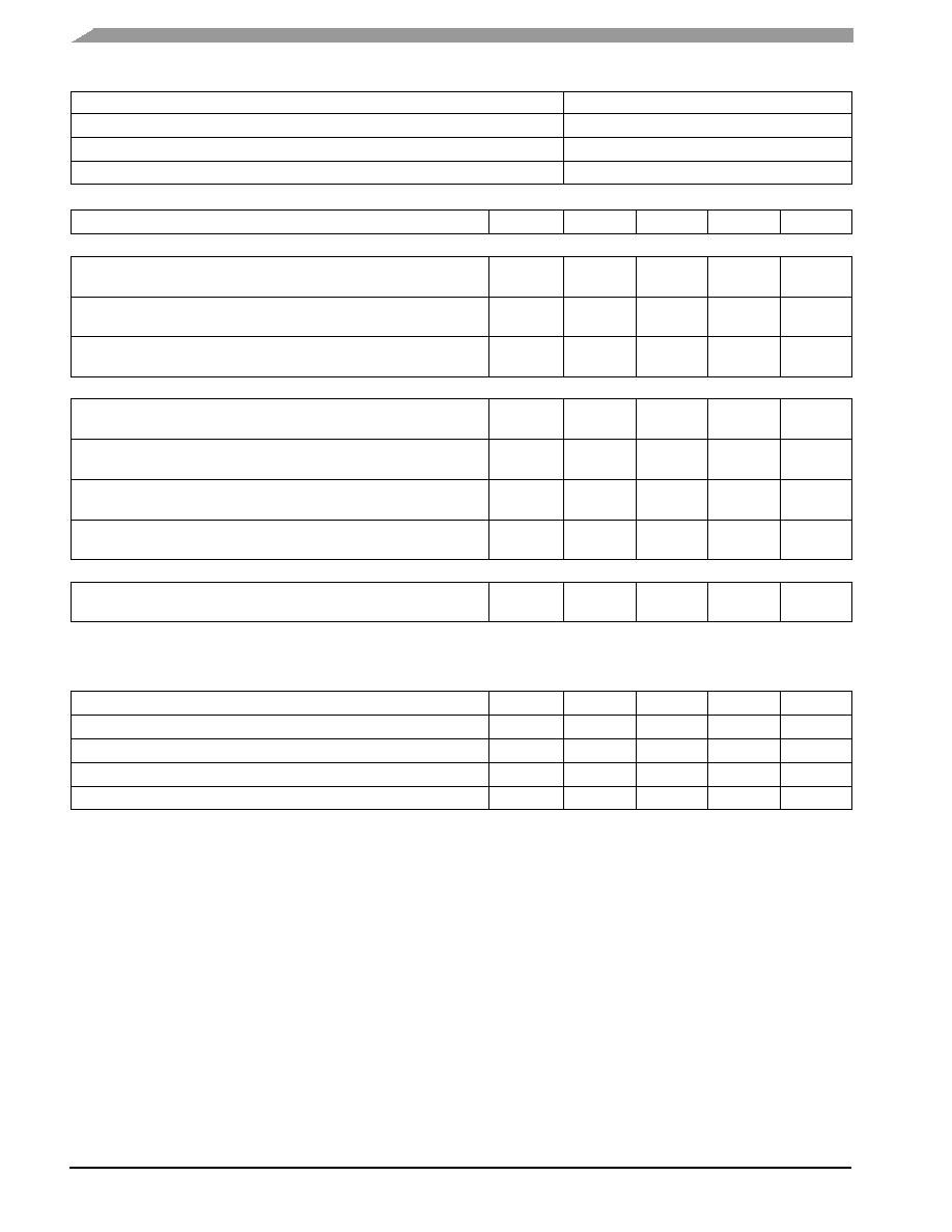
Table 1. Maximum Ratings
Rating
Symbol
Value
Unit
Drain-Source Voltage
V
DSS
-0.5, +68
Vdc
Gate-Source Voltage
V
GS
-0.5, +12
Vdc
Total Device Dissipation @ T
C
= 25∞C
Derate above 25∞C
P
D
330
1.9
W
W/∞C
Storage Temperature Range
T
stg
- 65 to +150
∞C
Operating Junction Temperature
T
J
200
∞C
CW Operation
CW
100
W
Table 2. Thermal Characteristics
Characteristic
Symbol
Value
(1,2)
Unit
Thermal Resistance, Junction to Case
Case Temperature 80∞C, 100 W CW
Case Temperature 75∞C, 20 W CW
R
JC
0.53
0.59
∞C/W
1. MTTF calculator available at http://www.freescale.com/rf. Select Tools/Software/Application Software/Calculators to access
the MTTF calculators by product.
2. Refer to AN1955, Thermal Measurement Methodology of RF Power Amplifiers. Go to http://www.freescale.com/rf.
Select Documentation/Application Notes - AN1955.
NOTE - CAUTION - MOS devices are susceptible to damage from electrostatic charge. Reasonable precautions in handling and
packaging MOS devices should be observed.
Document Number: MRF6S23100H
Rev. 0, 8/2005
Freescale Semiconductor
Technical Data
MRF6S23100HR3
MRF6S23100HSR3
2300 -2400 MHz, 20 W AVG., 28 V
2 x W-CDMA
LATERAL N-CHANNEL
RF POWER MOSFETs
CASE 465-06, STYLE 1
NI-780
MRF6S23100HR3
CASE 465A-06, STYLE 1
NI-780S
MRF6S23100HSR3
Freescale Semiconductor, Inc., 2005. All rights reserved.
2
RF Device Data
Freescale Semiconductor
MRF6S23100HR3 MRF6S23100HSR3
Table 3. ESD Protection Characteristics
Test Methodology
Class
Human Body Model (per JESD22-A114)
3A (Minimum)
Machine Model (per EIA/JESD22-A115)
A (Minimum)
Charge Device Model (per JESD22-C101)
IV (Minimum)
Table 4. Electrical Characteristics
(T
C
= 25∞C unless otherwise noted)
Characteristic
Symbol
Min
Typ
Max
Unit
Off Characteristics
Zero Gate Voltage Drain Leakage Current
(V
DS
= 68 Vdc, V
GS
= 0 Vdc)
I
DSS
--
--
10
µAdc
Zero Gate Voltage Drain Leakage Current
(V
DS
= 28 Vdc, V
GS
= 0 Vdc)
I
DSS
--
--
1
µAdc
Gate-Source Leakage Current
(V
GS
= 5 Vdc, V
DS
= 0 Vdc)
I
GSS
--
--
1
µAdc
On Characteristics
Gate Threshold Voltage
(V
DS
= 10 Vdc, I
D
= 250 µAdc)
V
GS(th)
1
2
3
Vdc
Gate Quiescent Voltage
(V
DS
= 28 Vdc, I
D
= 1000 mAdc)
V
GS(Q)
2
2.8
4
Vdc
Drain-Source On-Voltage
(V
GS
= 10 Vdc, I
D
= 2.2 Adc)
V
DS(on)
0.1
0.21
0.3
Vdc
Forward Transconductance
(V
DS
= 10 Vdc, I
D
= 2 Adc)
g
fs
--
5.3
--
S
Dynamic Characteristics
(1)
Reverse Transfer Capacitance
(V
DS
= 28 Vdc ± 30 mV(rms)ac @ 1 MHz, V
GS
= 0 Vdc)
C
rss
--
1.5
--
pF
Functional Tests (In Freescale Test Fixture, 50 ohm system) V
DD
= 28 Vdc, I
DQ
= 1000 mA, P
out
= 20 W Avg., f1 = 2300 MHz,
f2 = 2310 MHz and f1 = 2390 MHz, f2 = 2400 MHz, 2-Carrier W-CDMA, 3.84 MHz Channel Bandwidth Carriers. ACPR measured in
3.84 MHz Channel Bandwidth @ ±5 MHz Offset. IM3 measured in 3.84 MHz Bandwidth @ ±10 MHz Offset. PAR = 8.5 dB @ 0.01%
Probability on CCDF.
Power Gain
G
ps
14
15.4
17
dB
Drain Efficiency
D
22.5
23.5
--
%
Intermodulation Distortion
IM3
-35
-37
--
dBc
Adjacent Channel Power Ratio
ACPR
-38
-40.5
--
dBc
Input Return Loss
IRL
--
-10
--
dB
1. Part is internally matched both on input and output.
MRF6S23100HR3 MRF6S23100HSR3
3
RF Device Data
Freescale Semiconductor
Figure 1. MRF6S23100HR3(HSR3) Test Circuit Schematic
Z9
0.329 x 0.756 Microstrip
Z10
0.083 x 0.756 Microstrip
Z11
0.092 x 0.800 Microstrip
Z12
0.436 x 0.800 Microstrip
Z13
0.974 x 0.080 Microstrip
Z14
0.727 x 0.080 Microstrip
PCB
Arlon GX-0300-5022, 0.030,
r
= 2.5
Z1
0.725 x 0.080 Microstrip
Z2
0.240 x 0.080 Microstrip
Z3
0.110 x 0.240 Microstrip
Z4
0.140 x 0.080 Microstrip
Z5
0.167 x 0.500 Microstrip
Z6
0.130 x 0.080 Microstrip
Z7
0.250 x 0.611 Microstrip
Z8
0.060 x 0.080 Microstrip
V
BIAS
V
SUPPLY
RF
OUTPUT
RF
INPUT
DUT
C11
Z1
Z6
Z7
Z8
C1
C7
Z9
Z11
Z12
Z13
Z14
R1
C12
+
C6
+
B1
C10
C9
C8
Z10
Z2
Z3
Z4
Z5
C5
+
C4
C3
C2
Table 5. MRF6S23100HR3(HSR3) Test Circuit Component Designations and Values
Part
Description
Part Number
Manufacturer
B1
Ferrite Bead
2743019447
Fair-Rite
C1, C2, C7, C8
5.6 pF Chip Capacitors, B Case
100B5R6CP500X
ATC
C3
0.01 µF Chip Capacitor (1825)
C1825C103J1RAC
Kemet
C4, C9
2.2 µF, 50 V Chip Capacitors (1825)
C1825C225J5RAC
Kemet
C5
22 µF, 25 V Tantalum Capacitor
ECS-T1ED226R
Panasonic TE series
C6
47 µF, 16 V Tantalum Capacitor
T491D476K016AS
Kemet
C10, C11
10 µF, 50 V Chip Capacitors (2220)
GRM55DR61H106KA88B
Murata
C12
330 µF, 63 V Electrolytic Capacitor
NACZF331M63V
Nippon
R1
10 , 1/8 W Chip Resistor (1206)
CRC120610R0F100
Dale/Vishay
4
RF Device Data
Freescale Semiconductor
MRF6S23100HR3 MRF6S23100HSR3
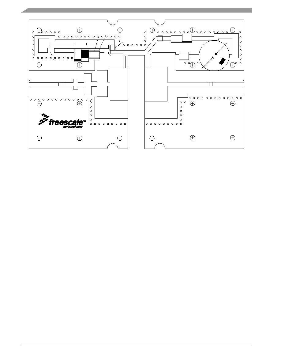
Figure 2. MRF6S23100HR3(HSR3) Test Circuit Component Layout
CUT
OUT
AREA
MRF6S23100 Rev 2.0
C10
C1
R1
B1
C6
C5
C4
C2
C8
C9
C11
C12
C7
C3
MRF6S23100HR3 MRF6S23100HSR3
5
RF Device Data
Freescale Semiconductor
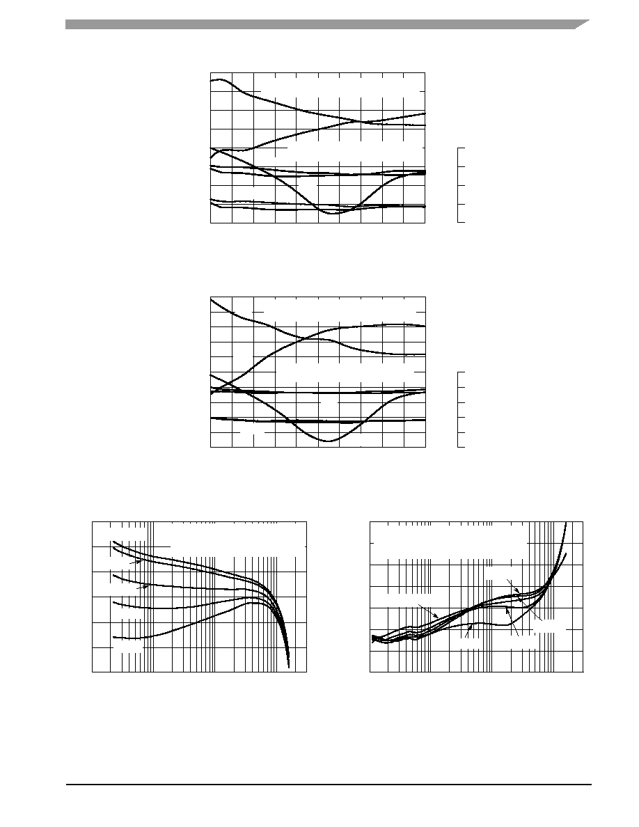
TYPICAL CHARACTERISTICS
G
ps
, POWER GAIN (dB)
IRL, INPUT RETURN LOSS (dB)
IM3 (dBc), ACPR (dBc)
-24
-12
-15
-21
2400
2300
IRL
G
ps
ACPR
IM3
f, FREQUENCY (MHz)
Figure 3. 2-Carrier W-CDMA Broadband Performance @ P
out
= 20 Watts Avg.
2370
2360
2350
2340
2330
2320
2310
16
-43
25.4
24.8
24.2
23.6
-35
-37
-39
D
, DRAIN
EFFICIENCY (%)
15.8
15.6
15.4
15.2
15
14.8
14.6
-41
-18
14.4
D
G
ps
, POWER GAIN (dB)
IRL, INPUT RETURN LOSS (dB)
IM3 (dBc), ACPR (dBc)
-22
-12
-16
2400
2300
IRL
G
ps
ACPR
IM3
f, FREQUENCY (MHz)
Figure 4. 2-Carrier W-CDMA Broadband Performance @ P
out
= 40 Watts Avg.
2370
2360
2350
2340
2330
2320
2310
15.2
-35
35.5
35
34.5
34
-27
-29
-31
D
, DRAIN
EFFICIENCY (%)
15.1
15
14.9
14.8
14.7
14.6
14.5
-25
-14
3.84 MHz Channel Bandwidth
PAR = 8.5 dB @ 0.01% Probability (CCDF)
14.2
D
Figure 5. Two-Tone Power Gain versus
Output Power
10
12
18
0.1
I
DQ
= 1500 mA
P
out
, OUTPUT POWER (WATTS) PEP
300
G
ps
, POWER GAIN (dB)
16
15
13
1000 mA
750 mA
500 mA
14
100
V
DD
= 28 Vdc, f1 = 2345 MHz
f2 = 2355
MHz, Two-Tone Measurements
10 MHz Tone Spacing
Figure 6. Third Order Intermodulation Distortion
versus Output Power
0
0.1
10
-20
-30
-40
300
-70
-50
P
out
, OUTPUT POWER (WATTS) PEP
INTERMODULA
TION DIST
ORTION
(dBc)
IMD, THIRD ORDER
100
-18
-20
2380 2390
14.4
14.3
2380 2390
35.5
-33
1250 mA
-10
-60
1
1
I
DQ
= 500 mA
1000 mA
750 mA
V
DD
= 28 Vdc
f1 = 2345 MHz, f2 = 2355
MHz
Two-Tone Measurements, 10 MHz Tone Spacing
1500 mA
1250 mA
17
3.84 MHz Channel Bandwidth
PAR = 8.5 dB @ 0.01% Probability (CCDF)
V
DD
= 28 Vdc, P
out
= 20 W (Avg.), I
DQ
= 1000 mA
2-Carrier W-CDMA, 10 MHz Carrier Spacing
V
DD
= 28 Vdc, P
out
= 40 W (Avg.), I
DQ
= 1000 mA
2-Carrier W-CDMA, 10 MHz Carrier Spacing