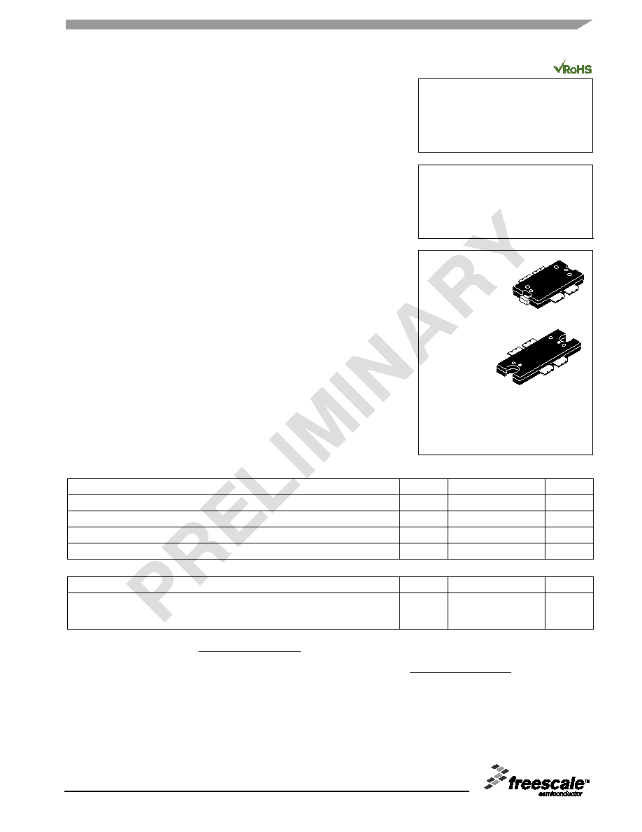
MRF6V2300N MRF6V2300NB
1
RF Device Data
Freescale Semiconductor
RF Power Field Effect Transistor
N-Channel Enhancement-Mode Lateral MOSFETs
Designed primarily for pulsed wideband large - signal output and driver
applications with frequencies up to 450 MHz. Devices are unmatched and are
suitable for use in industrial, medical and scientific applications.
∑ Typical CW Performance at 220 MHz: V
DD
= 50 Volts, I
DQ
= 900 mA,
P
out
= 300 Watts
Power Gain -- 27
dB
Drain Efficiency -- 68%
∑ Capable of Handling 10:1 VSWR, @ 50 Vdc, 210 MHz, 300 Watts CW
Output Power
Features
∑ Integrated ESD Protection
∑ Greater Negative Gate-Source Voltage Range for Improved Class C
Operation
∑ Excellent Thermal Stability
∑ Facilitates Manual Gain Control, ALC and Modulation Techniques
∑ 225∞C Capable Plastic Package
∑ RoHS Compliant
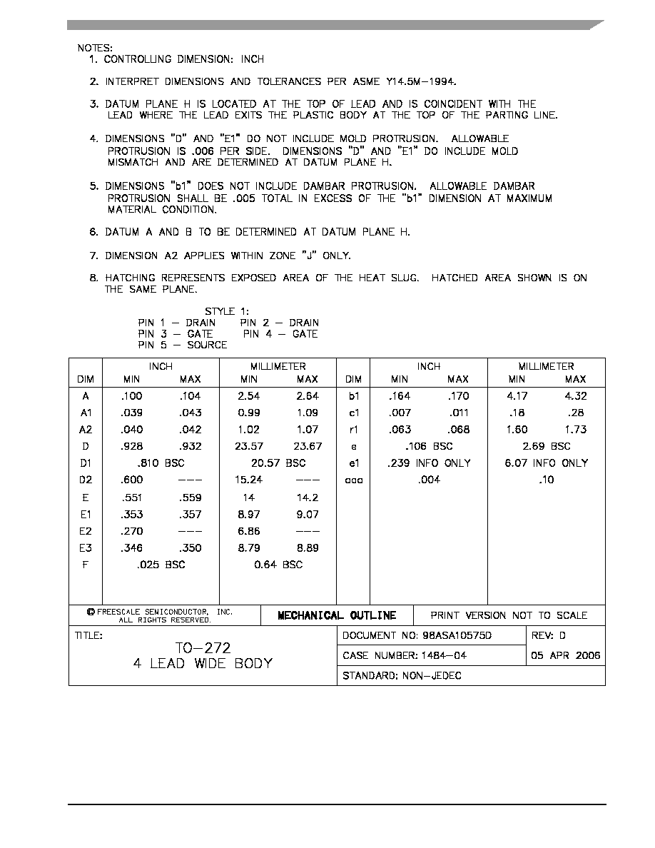
Table 1. Maximum Ratings
Rating
Symbol
Value
Unit
Drain-Source Voltage
V
DSS
-0.5, +110
Vdc
Gate-Source Voltage
V
GS
-6.0, +10
Vdc
Storage Temperature Range
T
stg
- 65 to +150
∞C
Operating Junction Temperature
(1,2)
T
J
225
∞C
Table 2. Thermal Characteristics
Characteristic
Symbol
Value
(3)
Unit
Thermal Resistance, Junction to Case
Case Temperature TBD∞C, TBD W CW
Case Temperature TBD∞C, TBD W CW
R
JC
TBD
TBD
∞C/W
1. Continuous use at maximum temperature will affect MTTF.
2. MTTF calculator available at http://www.freescale.com/rf. Select Tools/Software/Application Software/Calculators to access
the MTTF calculators by product. (Calculator available when part is in production.)
3. Refer to AN1955, Thermal Measurement Methodology of RF Power Amplifiers. Go to http://www.freescale.com/rf.
Select Documentation/Application Notes - AN1955.
This document contains information on a preproduction product. Specifications and information herein are subject to change without notice.
Document Number: Order from RF Marketing
Rev. 4, 10/2006
Freescale Semiconductor
Technical Data
MRF6V2300N
MRF6V2300NB
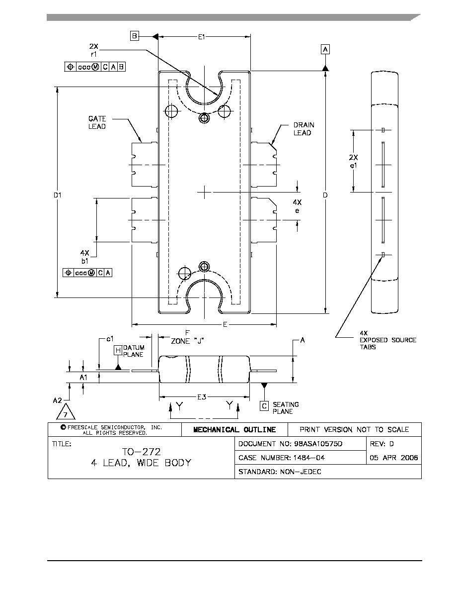
CASE 1484-04, STYLE 1
TO-272 WB-4
PLASTIC
MRF6V2300NB
PREPRODUCTION
CASE 1486-03, STYLE 1
TO-270 WB-4
PLASTIC
MRF6V2300N
10-450 MHz, 300 W, 50 V
LATERAL N-CHANNEL
SINGLE-ENDED
BROADBAND
RF POWER MOSFETs
PARTS ARE SINGLE-ENDED
© Freescale Semiconductor, Inc., 2006. All rights reserved.
2
RF Device Data
Freescale Semiconductor
MRF6V2300N MRF6V2300NB
Table 3. ESD Protection Characteristics
Test Methodology
Class
Human Body Model (per JESD22-A114)
TBD (Minimum)
Machine Model (per EIA/JESD22-A115)
TBD (Minimum)
Charge Device Model (per JESD22-C101)
TBD (Minimum)
Table 4. Moisture Sensitivity Level
Test Methodology
Rating
Package Peak Temperature
Unit
Per JESD 22-A113, IPC/JEDEC J-STD-020
3
260
∞C
Table 5. Electrical Characteristics
(T
C
= 25∞C unless otherwise noted)
Characteristic
Symbol
Min
Typ
Max
Unit
Off Characteristics
Zero Gate Voltage Drain Leakage Current
(V
DS
= 110 Vdc, V
GS
= 0 Vdc)
I
DSS
--
--
10
Adc
Zero Gate Voltage Drain Leakage Current
(V
DS
= 50 Vdc, V
GS
= 0 Vdc)
I
DSS
--
--
10
Adc
Drain-Source Breakdown Voltage
(I
D
= 150 mA, V
GS
= 0 Vdc)
BV
DSS
110
--
--
Vdc
Gate-Source Leakage Current
(V
GS
= 5 Vdc, V
DS
= 0 Vdc)
I
GSS
--
--
10
Adc
On Characteristics
Gate Threshold Voltage
(V
DS
= 10 Vdc, I
D
= 800 Adc)
V
GS(th)
--
2.4
--
Vdc
Drain-Source On-Voltage
(V
GS
= 10 Vdc, I
D
= 2 Adc)
V
DS(on)
--
0.3
--
Vdc
Dynamic Characteristics
Reverse Transfer Capacitance
(V
DS
= 50
Vdc ± 30 mV(rms)ac @ 1 MHz, V
GS
= 0 Vdc)
C
rss
--
2.44
--
pF
Output Capacitance
(V
DS
= 50
Vdc ± 30 mV(rms)ac @ 1 MHz, V
GS
= 0 Vdc)
C
oss
--
120
--
pF
Input Capacitance
(V
DS
= 50
Vdc ± 30 mV(rms)ac @ 1 MHz, V
GS
= 0 Vdc)
C
iss
--
282
--
pF
Functional Tests (In Freescale Test Fixture, 50 ohm system) V
DD
= 50 Vdc, I
DQ
= 900 mA, P
out
= 300
W, f = 220 MHz, CW
Power Gain
G
ps
--
27
--
dB
Drain Efficiency
D
--
68
--
%
Input Return Loss
IRL
--
-17
--
dB
P
out
@ 1 dB Compression Point, CW
(f = 220 MHz)
P1dB
--
330
--
W
ATTENTION: The MRF6V2300N and MRF6V2300NB are high power devices and special considerations
must be followed in board design and mounting. Incorrect mounting can lead to internal temperatures which
exceed the maximum allowable operating junction temperature. Refer to Freescale Application Note AN3263
(for bolt down mounting) or AN1907 (for solder reflow mounting) PRIOR TO STARTING SYSTEM DESIGN to
ensure proper mounting of these devices.
MRF6V2300N MRF6V2300NB
3
RF Device Data
Freescale Semiconductor
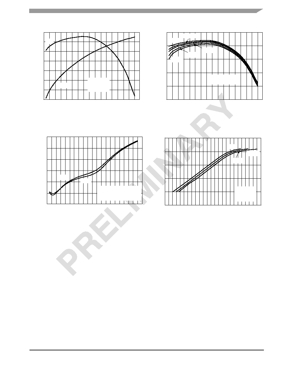
TYPICAL CHARACTERISTICS
400
24
27.5
0
10
80
V
DD
= 50 Vdc
I
DQ
= 900 mA
f = 220 MHz
100
50
27
26
25
70
60
50
40
30
20
P
out
, OUTPUT POWER (WATTS) CW
Figure 1. Power Gain and Drain Efficiency
versus CW Output Power
G
ps
, POWER GAIN (dB)
D,
DRAIN EFFICIENCY (%)
150
G
ps
D
400
23
28
0
V
DD
= 50 Vdc
f = 220 MHz
100
50
27
26
25
24
P
out
, OUTPUT POWER (WATTS) CW
Figure 2. Power Gain versus Output Power
G
ps
, POWER GAIN (dB)
150
I
DQ
= 990 mA
1090 mA
720 mA
810 mA
900 mA
100
-50
-20
0
P
out
, OUTPUT POWER (WATTS) PEP
-25
-30
-35
-40
50
200
Figure 3. Third Order Intermodulation
Distortion versus Output Power
IMD,
THIRD ORDER INTERMODULA
TION
DIST
ORTION (dBc)
150
V
DD
= 50 Vdc, I
DQ
= 900 mA
f1 = 220 MHz, f2 = 220.1 MHz
Two-Tone Measurements
35
35
60
10
25_C
-30_C
85_C
25
15
50
45
40
P
in
, INPUT POWER (dBm)
Figure 4. Output Power versus Input Power
over Temperature
P
out
, OUTPUT POWER (dBm)
V
DD
= 50 Vdc
I
DQ
= 900 mA
f = 220 MHz
20
30
26.5
25.5
24.5
200
250
300
350
200
250
300
350
55
-45
IM3-L
IM3-U
4
RF Device Data
Freescale Semiconductor
MRF6V2300N MRF6V2300NB
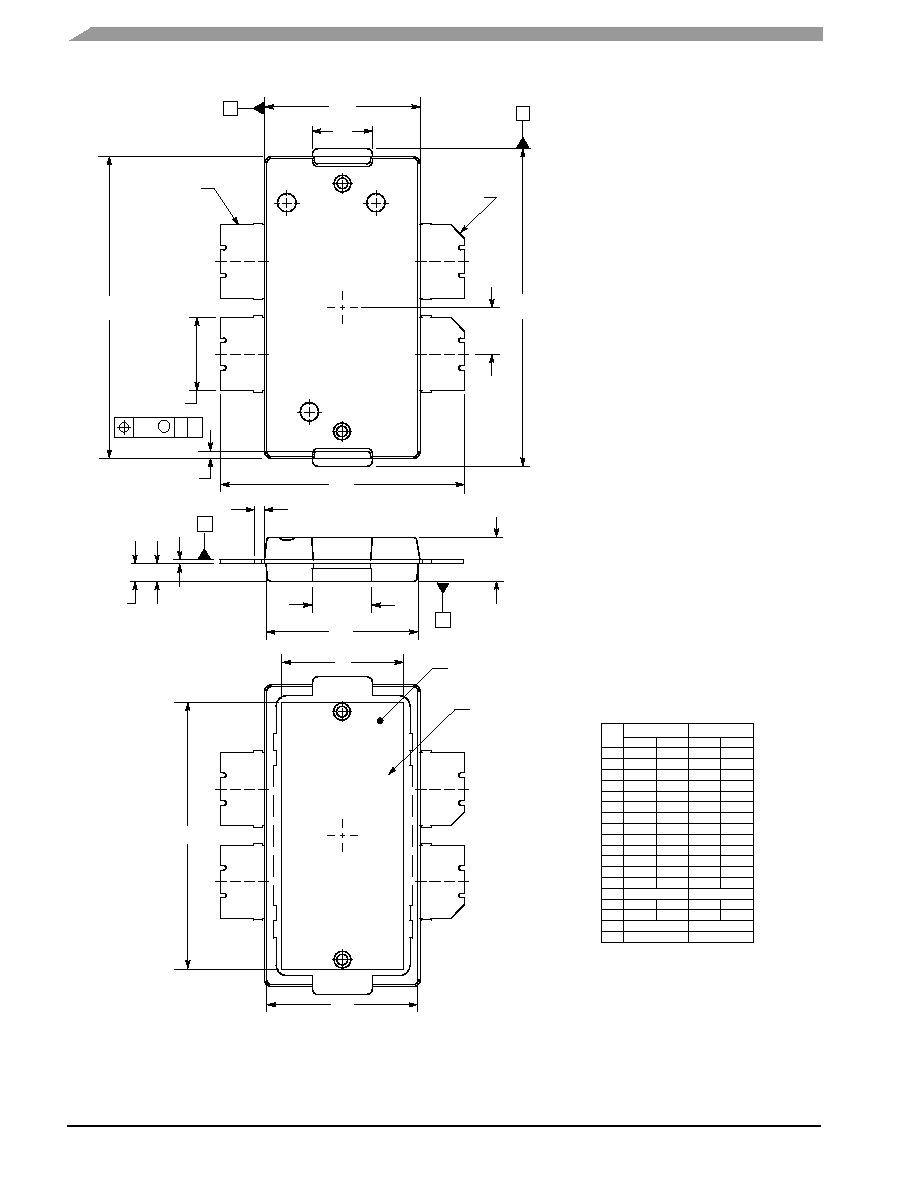
PACKAGE DIMENSIONS
CASE 1486-03
ISSUE C
DATUM
PLANE
BOTTOM VIEW
A1
2X
D1
E3
E1
D3
E4
A2
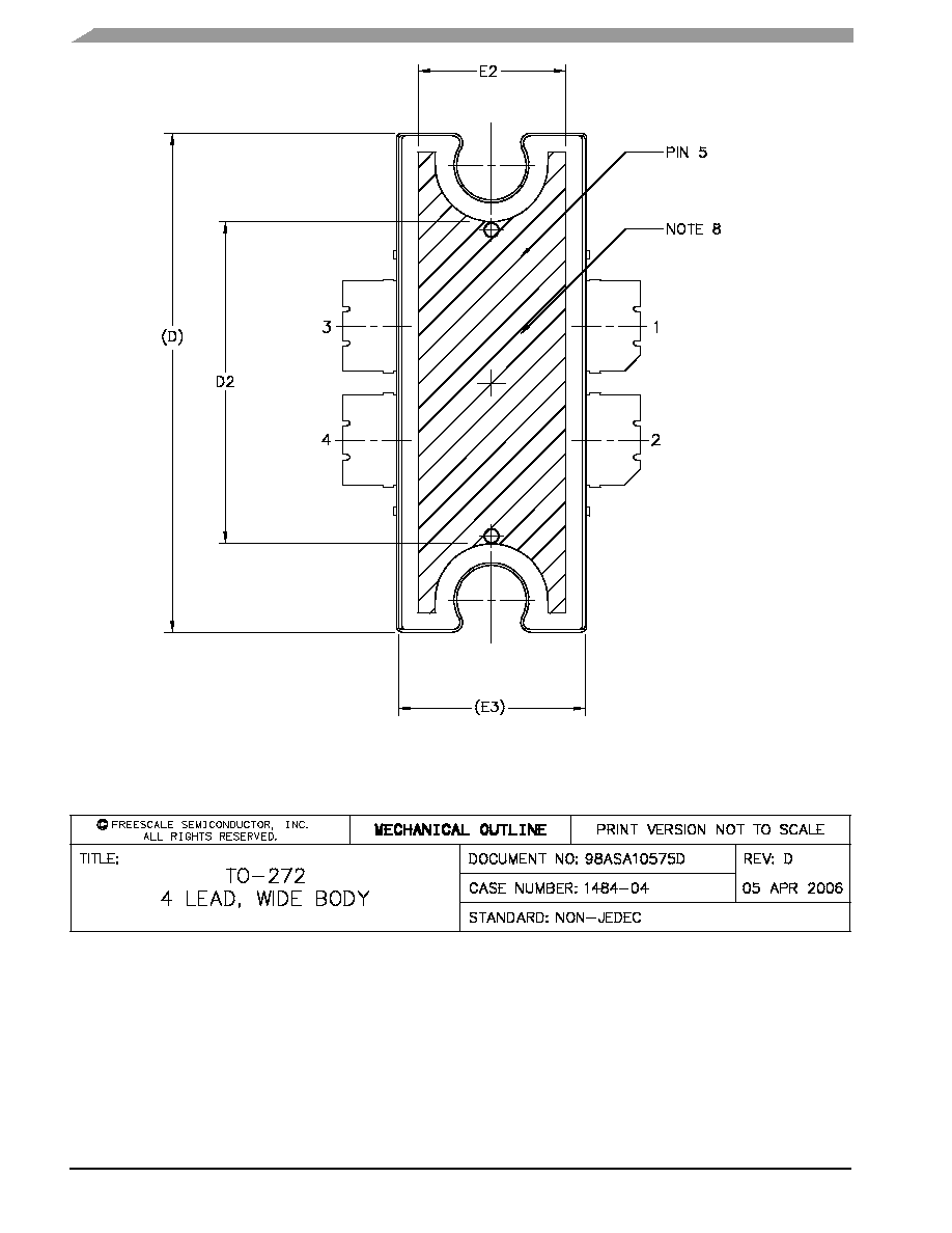
PIN 5
NOTE 8
A
B
C
H
DRAIN LEAD
D
A
M
aaa
C
4X
b1
2X
D2
NOTES:
1. CONTROLLING DIMENSION: INCH.
2. INTERPRET DIMENSIONS AND TOLERANCES
PER ASME Y14.5M-1994.
3. DATUM PLANE -H- IS LOCATED AT THE TOP OF
LEAD AND IS COINCIDENT WITH THE LEAD
WHERE THE LEAD EXITS THE PLASTIC BODY AT
THE TOP OF THE PARTING LINE.
4. DIMENSIONS "D" AND "E1" DO NOT INCLUDE
MOLD PROTRUSION. ALLOWABLE PROTRUSION
IS .006 PER SIDE. DIMENSIONS "D" AND "E1" DO
INCLUDE MOLD MISMATCH AND ARE DETER-
MINED AT DATUM PLANE -H-.
5. DIMENSION "b1" DOES NOT INCLUDE DAMBAR
PROTRUSION. ALLOWABLE DAMBAR
PROTRUSION SHALL BE .005 TOTAL IN EXCESS
OF THE "b1" DIMENSION AT MAXIMUM MATERIAL
CONDITION.
6. DATUMS -A- AND -B- TO BE DETERMINED AT
DATUM PLANE -H-.
7. DIMENSION A2 APPLIES WITHIN ZONE "J" ONLY.
8. HATCHING REPRESENTS THE EXPOSED AREA
OF THE HEAT SLUG.
c1
F
ZONE J
E2
2X
A
DIM
A
MIN
MAX
MIN
MAX
MILLIMETERS
.100
.104
2.54
2.64
INCHES
A1
.039
.043
0.99
1.09
A2
.040
.042
1.02
1.07
D
.712
.720
18.08
18.29
D1
.688
.692
17.48
17.58
D2
.011
.019
0.28
0.48
D3
.600
- - -
15.24
- - -
E
.551
.559
14
14.2
E1
.353
.357
8.97
9.07
E2
.132
.140
3.35
3.56
E3
.124
.132
3.15
3.35
E4
.270
- - -
6.86
- - -
F
b1
.164
.170
4.17
4.32
c1
.007
.011
0.18
0.28
e
.025 BSC
.106 BSC
0.64 BSC
2.69 BSC
1
STYLE 1:
PIN 1. DRAIN
2. DRAIN
3. GATE
4. GATE
5. SOURCE
aaa
.004
0.10
GATE LEAD
4X
e
2X
E
SEATING
PLANE
4
2
3
««««««
««««««
««««««
««««««
««««««
««««««
««««««
««««««
««««««
««««««
««««««
««««««
««««««
NOTE 7
E5
E5
E5
.346
.350
8.79
8.89
TO-270 WB-4
PLASTIC
MRF6V2300N
MRF6V2300N MRF6V2300NB
5
RF Device Data
Freescale Semiconductor
6
RF Device Data
Freescale Semiconductor
MRF6V2300N MRF6V2300NB
MRF6V2300N MRF6V2300NB
7
RF Device Data
Freescale Semiconductor

8
RF Device Data
Freescale Semiconductor
MRF6V2300N MRF6V2300NB
Information in this document is provided solely to enable system and software
implementers to use Freescale Semiconductor products. There are no express or
implied copyright licenses granted hereunder to design or fabricate any integrated
circuits or integrated circuits based on the information in this document.
Freescale Semiconductor reserves the right to make changes without further notice to
any products herein. Freescale Semiconductor makes no warranty, representation or
guarantee regarding the suitability of its products for any particular purpose, nor does
Freescale Semiconductor assume any liability arising out of the application or use of
any product or circuit, and specifically disclaims any and all liability, including without
limitation consequential or incidental damages. "Typical" parameters that may be
provided in Freescale Semiconductor data sheets and/or specifications can and do
vary in different applications and actual performance may vary over time. All operating
parameters, including "Typicals", must be validated for each customer application by
customer's technical experts. Freescale Semiconductor does not convey any license
under its patent rights nor the rights of others. Freescale Semiconductor products are
not designed, intended, or authorized for use as components in systems intended for
surgical implant into the body, or other applications intended to support or sustain life,
or for any other application in which the failure of the Freescale Semiconductor product
could create a situation where personal injury or death may occur. Should Buyer
purchase or use Freescale Semiconductor products for any such unintended or
unauthorized application, Buyer shall indemnify and hold Freescale Semiconductor
and its officers, employees, subsidiaries, affiliates, and distributors harmless against all
claims, costs, damages, and expenses, and reasonable attorney fees arising out of,
directly or indirectly, any claim of personal injury or death associated with such
unintended or unauthorized use, even if such claim alleges that Freescale
Semiconductor was negligent regarding the design or manufacture of the part.
Freescalet and the Freescale logo are trademarks of Freescale Semiconductor, Inc.
All other product or service names are the property of their respective owners.
© Freescale Semiconductor, Inc. 2006. All rights reserved.
How to Reach Us:
Home Page:
www.freescale.com
E-mail:
support@freescale.com
USA/Europe or Locations Not Listed:
Freescale Semiconductor
Technical Information Center, CH370
1300 N. Alma School Road
Chandler, Arizona 85224
+1-800-521-6274 or +1-480-768-2130
support@freescale.com
Europe, Middle East, and Africa:
Freescale Halbleiter Deutschland GmbH
Technical Information Center
Schatzbogen 7
81829 Muenchen, Germany
+44 1296 380 456 (English)
+46 8 52200080 (English)
+49 89 92103 559 (German)
+33 1 69 35 48 48 (French)
support@freescale.com
Japan:
Freescale Semiconductor Japan Ltd.
Headquarters
ARCO Tower 15F
1-8-1, Shimo-Meguro, Meguro-ku,
Tokyo 153-0064
Japan
0120 191014 or +81 3 5437 9125
support.japan@freescale.com
Asia/Pacific:
Freescale Semiconductor Hong Kong Ltd.
Technical Information Center
2 Dai King Street
Tai Po Industrial Estate
Tai Po, N.T., Hong Kong
+800 2666 8080
support.asia@freescale.com
For Literature Requests Only:
Freescale Semiconductor Literature Distribution Center
P.O. Box 5405
Denver, Colorado 80217
1-800-441-2447 or 303-675-2140
Fax: 303-675-2150
LDCForFreescaleSemiconductor@hibbertgroup.com
Document Number: Order from RF Marketing
Rev. 4, 10/2006