
1
MRF9030MR1 MRF9030MBR1
MOTOROLA RF DEVICE DATA
The RF Sub-Micron MOSFET Line
RF Power Field Effect Transistors
N-Channel Enhancement-Mode Lateral MOSFETs
Designed for broadband commercial and industrial applications with frequen-
cies up to 1.0 GHz. The high gain and broadband performance of these devices
make them ideal for large-signal, common-source amplifier applications in
26 volt base station equipment.
∑ Typical Performance at 945 MHz, 26 Volts
Output Power -- 30 Watts PEP
Power Gain -- 20 dB
Efficiency -- 41% (Two Tones)
IMD -- -31 dBc
∑ Integrated ESD Protection
∑ Capable of Handling 5:1 VSWR, @ 26 Vdc, 945 MHz, 30 Watts (CW)
Output Power
∑ Excellent Thermal Stability
∑ Characterized with Series Equivalent Large-Signal Impedance Parameters
∑ Dual-Lead Boltdown Plastic Package Can Also Be Used As Surface
Mount.
∑ TO-272-2 in Tape and Reel. R1 Suffix = 500 Units per 44 mm,
13 inch Reel.
∑ TO-270-2 in Tape and Reel. R1 Suffix = 500 Units per 24 mm,
13 inch Reel.
MAXIMUM RATINGS
Rating
Symbol
Value
Unit
Drain-Source Voltage
V
DSS
65
Vdc
Gate-Source Voltage
V
GS
+ 15, -0.5
Vdc
Total Device Dissipation @ T
C
= 25∞C
Derate above 25∞C
P
D
139
0.93
Watts
W/∞C
Storage Temperature Range
T
stg
-65 to +150
∞C
Operating Junction Temperature
T
J
175
∞C
THERMAL CHARACTERISTICS
Characteristic
Symbol
Max
Unit
Thermal Resistance, Junction to Case
R
JC
1.08
∞C/W
ESD PROTECTION CHARACTERISTICS
Test Conditions
Class
Human Body Model
1 (Minimum)
Machine Model
M2 (Minimum)
Charge Device Model
MRF9030MR1
MRF9030MBR1
C7 (Minimum)
C6 (Minimum)
MOISTURE SENSITIVITY LEVEL
Test Methodology
Rating
Per JESD 22-A113
3
NOTE - CAUTION - MOS devices are susceptible to damage from electrostatic charge. Reasonable precautions in handling and
packaging MOS devices should be observed.
Order this document
by MRF9030M/D
MOTOROLA
SEMICONDUCTOR TECHNICAL DATA
MRF9030MR1
MRF9030MBR1
945 MHz, 30 W, 26 V
LATERAL N-CHANNEL
BROADBAND
RF POWER MOSFETs
CASE 1337-03, STYLE 1
TO-272-2
PLASTIC
MRF9030MBR1
CASE 1265-08, STYLE 1
TO-270-2
PLASTIC
MRF9030MR1
Motorola, Inc. 2003
REV 6
F
r
e
e
s
c
a
l
e
S
e
m
i
c
o
n
d
u
c
t
o
r
,
I
Freescale Semiconductor, Inc.
For More Information On This Product,
Go to: www.freescale.com
n
c
.
.
.

MRF9030MR1 MRF9030MBR1
2
MOTOROLA RF DEVICE DATA
ELECTRICAL CHARACTERISTICS
(T
C
= 25∞C unless otherwise noted)
Characteristic
Symbol
Min
Typ
Max
Unit
OFF CHARACTERISTICS
Zero Gate Voltage Drain Leakage Current
(V
DS
= 65 Vdc, V
GS
= 0 Vdc)
I
DSS
--
--
10
µAdc
Zero Gate Voltage Drain Leakage Current
(V
DS
= 26 Vdc, V
GS
= 0 Vdc)
I
DSS
--
--
1
µAdc
Gate-Source Leakage Current
(V
GS
= 5 Vdc, V
DS
= 0 Vdc)
I
GSS
--
--
1
µAdc
ON CHARACTERISTICS
Gate Threshold Voltage
(V
DS
= 10 Vdc, I
D
= 100 µAdc)
V
GS(th)
2
2.9
4
Vdc
Gate Quiescent Voltage
(V
DS
= 26 Vdc, I
D
= 250 mAdc)
V
GS(Q)
3
3.8
5
Vdc
Drain-Source On-Voltage
(V
GS
= 10 Vdc, I
D
= 0.7 Adc)
V
DS(on)
--
0.23
0.4
Vdc
Forward Transconductance
(V
DS
= 10 Vdc, I
D
= 2 Adc)
g
fs
--
2.7
--
S
DYNAMIC CHARACTERISTICS
Input Capacitance
(V
DS
= 26 Vdc ± 30 mV(rms)ac @ 1 MHz, V
GS
= 0 Vdc)
C
iss
--
49
--
pF
Output Capacitance
(V
DS
= 26 Vdc ± 30 mV(rms)ac @ 1 MHz, V
GS
= 0 Vdc)
C
oss
--
27
--
pF
Reverse Transfer Capacitance
(V
DS
= 26 Vdc ± 30 mV(rms)ac @ 1 MHz, V
GS
= 0 Vdc)
C
rss
--
1.2
--
pF
FUNCTIONAL TESTS
(In Motorola Test Fixture)
Two-Tone Common-Source Amplifier Power Gain
(V
DD
= 26 Vdc, P
out
= 30 W PEP, I
DQ
= 250 mA,
f1 = 945.0 MHz, f2 = 945.1 MHz)
G
ps
18
20
--
dB
Two-Tone Drain Efficiency
(V
DD
= 26 Vdc, P
out
= 30 W PEP, I
DQ
= 250 mA,
f1 = 945.0 MHz, f2 = 945.1 MHz)
37
41
--
%
3rd Order Intermodulation Distortion
(V
DD
= 26 Vdc, P
out
= 30 W PEP, I
DQ
= 250 mA,
f1 = 945.0 MHz, f2 = 945.1 MHz)
IMD
--
-31
-28
dBc
Input Return Loss
(V
DD
= 26 Vdc, P
out
= 30 W PEP, I
DQ
= 250 mA,
f1 = 945.0 MHz, f2 = 945.1 MHz)
IRL
--
-13
-9
dB
Two-Tone Common-Source Amplifier Power Gain
(V
DD
= 26 Vdc, P
out
= 30 W PEP, I
DQ
= 250 mA,
f1 = 930.0 MHz, f2 = 930.1 MHz and f1 = 960.0 MHz,
f2 = 960.1 MHz)
G
ps
--
20
--
dB
Two-Tone Drain Efficiency
(V
DD
= 26 Vdc, P
out
= 30 W PEP, I
DQ
= 250 mA,
f1 = 930.0 MHz, f2 = 930.1 MHz and f1 = 960.0 MHz,
f2 = 960.1 MHz)
--
40.5
--
%
3rd Order Intermodulation Distortion
(V
DD
= 26 Vdc, P
out
= 30 W PEP, I
DQ
= 250 mA,
f1 = 930.0 MHz, f2 = 930.1 MHz and f1 = 960.0 MHz,
f2 = 960.1 MHz)
IMD
--
-31
--
dBc
Input Return Loss
(V
DD
= 26 Vdc, P
out
= 30 W PEP, I
DQ
= 250 mA,
f1 = 930.0 MHz, f2 = 930.1 MHz and f1 = 960.0 MHz,
f2 = 960.1 MHz)
IRL
--
-12
--
dB
F
r
e
e
s
c
a
l
e
S
e
m
i
c
o
n
d
u
c
t
o
r
,
I
Freescale Semiconductor, Inc.
For More Information On This Product,
Go to: www.freescale.com
n
c
.
.
.
3
MRF9030MR1 MRF9030MBR1
MOTOROLA RF DEVICE DATA
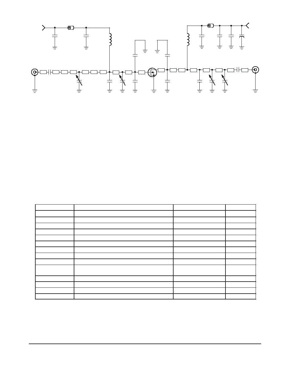
Figure 1. 930-960 MHz Broadband Test Circuit Schematic
Z1
0.260 x 0.060 Microstrip
Z2
0.240 x 0.060 Microstrip
Z3
0.500 x 0.100 Microstrip
Z4
0.200 x 0.270 Microstrip
Z5
0.330 x 0.270 Microstrip
Z6
0.140 x 0.270 x 0.520, Taper
Z7
0.040 x 0.520 Microstrip
Z8
0.090 x 0.520 Microstrip
Z9
0.370 x 0.520 Microstrip (MRF9030MR1)
0.290 x 0.520 Microstrip (MRF9030MBR1)
Z10
0.130 x 0.520 Microstrip (MRF9030MR1)
0.210 x 0.520 Microstrip (MRF9030MBR1)
Z11
0.360 x 0.270 Microstrip
Z12
0.050 x 0.270 Microstrip
Z13
0.110 x 0.060 Microstrip
Z14
0.220 x 0.060 Microstrip
Z15
0.100 x 0.060 Microstrip
Z16
0.870 x 0.060 Microstrip
Z17
0.240 x 0.060 Microstrip
Z18
0.340 x 0.060 Microstrip
Board
Taconic RF-35-0300,
r
= 3.5
Z14
C18
RF
INPUT
RF
OUTPUT
Z1
Z2
V
GG
C1
L1
V
DD
Z3
Z10
Z11
Z9
L2
B2
Z4
Z13
C16
B1
C8
C2
C5
C17
C9
Z15
Z18
C14
+
+
+
+
DUT
C7
C15
C3
C4
C6
C10
C11
C12
Z16
Z17
Z8
C13
Z5
Z6
Z7
Z12
Table 1. 930 - 960 MHz Broadband Test Circuit Component Designations and Values
Part
Description
Value, P/N or DWG
Manufacturer
B1
Short Ferrite Bead, Surface Mount
95F786
Newark
B2
Long Ferrite Bead, Surface Mount
95F787
Newark
C1, C7, C14, C15
47 pF Chip Capacitors, B Case
100B470JP 500X
ATC
C2
0.6-4.5 Variable Capacitor, Gigatrim
44F3360
Newark
C3, C11
3.9 pF Chip Capacitors, B Case
100B3R6BP 500X
ATC
C4, C12
0.8-8.0 Variable Capacitors, Gigatrim
44F3360
Newark
C5, C6
6.8 pF Chip Capacitors, B Case
100B7R5JP 500X
ATC
C8, C16, C17
10 µF, 35 V Tantulum Chip Capacitors
93F2975
Newark
C9, C10
10 pF Chip Capacitors, B Case
100B100JP 500X
ATC
C13
1.8 pF Chip Capacitor, B Case (MRF9030MR1)
0.6-4.5 Variable Capacitor, Gigatrim (MRF9030MBR1)
100B1R8BP
44F3360
ATC
Newark
C18
220 µF Electrolytic Chip Capacitor
14F185
Newark
L1, L2
12.5 nH Coilcraft Inductors
A04T-5
Coilcraft
WB1, WB2
20 mil Brass Shim (0.250 x 0.250)
RF-Design Lab
RF-Design Lab
PCB
Etched Circuit Board
900 MHz µ250/Viper Rev 02
DSelectronics
F
r
e
e
s
c
a
l
e
S
e
m
i
c
o
n
d
u
c
t
o
r
,
I
Freescale Semiconductor, Inc.
For More Information On This Product,
Go to: www.freescale.com
n
c
.
.
.
MRF9030MR1 MRF9030MBR1
4
MOTOROLA RF DEVICE DATA
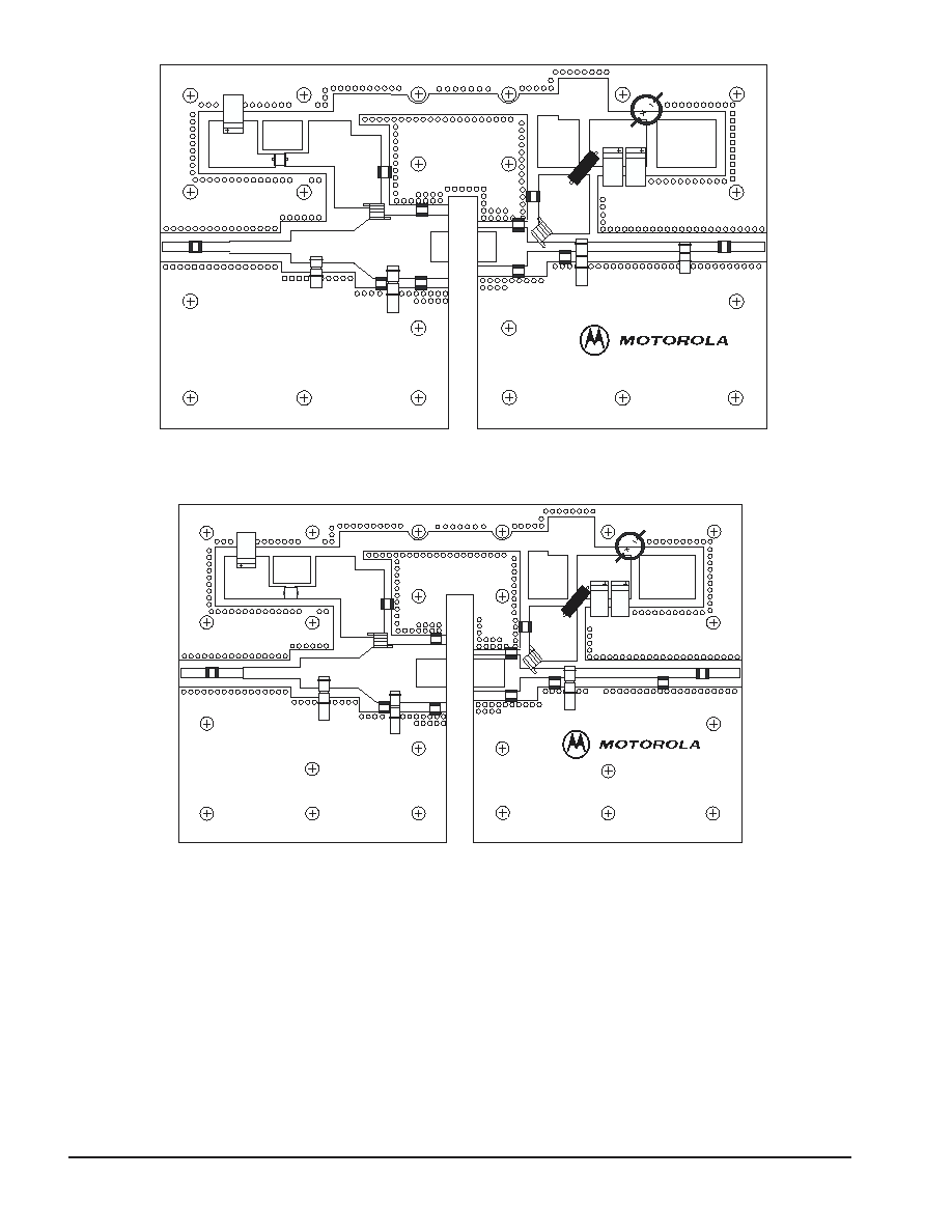
Figure 2. 930-960 MHz Broadband Test Circuit Component Layout (MRF9030MR1)
900 MHz
CUT
OUT
AREA
Rev 02
V
GG
V
DD
B1
B2
C1
C2
C3
C4
C5
C6
C7
C8
C9
C10
C11
C12
C13
C14
C15
C16 C17
C18
WB1
WB2
L1
L2
Figure 3. 930-960 MHz Broadband Test Circuit Component Layout (MRF9030MBR1)
C1
C2
C3
C5
C8
C7
C9
C10
C6
C11 C12
C14
C15
C16 C17
C18
L1
L2
MRF9030M
C4
CUT
OUT
AREA
B1
B2
C13
WB1
WB2
V
GG
V
DD
F
r
e
e
s
c
a
l
e
S
e
m
i
c
o
n
d
u
c
t
o
r
,
I
Freescale Semiconductor, Inc.
For More Information On This Product,
Go to: www.freescale.com
n
c
.
.
.
5
MRF9030MR1 MRF9030MBR1
MOTOROLA RF DEVICE DATA
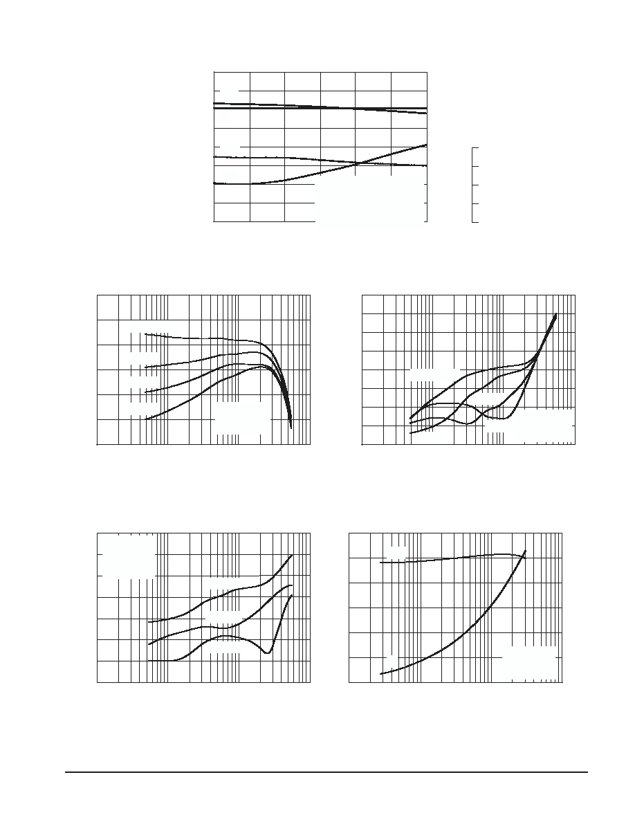
TYPICAL CHARACTERISTICS
G
ps
960
14
22
930
-38
50
IRL
IMD
V
DD
= 26 Vdc
P
out
= 30 W (PEP)
I
DQ
= 250 mA
Two-Tone, 100 kHz Tone Spac
ing
f, FREQUENCY (MHz)
Figure 4. Class AB Broadband Circuit Performance
G
ps
, POWER GAIN (dB)
-10
-18
-14
, DRAIN
h
EFFICIENCY
(%)
IMD, INTERMODUL
A
TION
DIST
ORTION (dBc)
IRL
, INPUT
RETURN
L
OSS (dB)
-12
-16
21
45
20
40
19
35
18
-30
17
-32
16
-34
15
-36
955
950
945
940
935
100
18.5
21.5
0.1
I
DQ
= 375 mA
300 mA
V
DD
= 26 Vdc
f1 = 945 MHz
f2 = 945.1 MHz
P
out
, OUTPUT POWER (WATTS) PEP
Figure 5. Power Gain versus Output Power
G
ps
, POWER GAIN (dB)
21
20.5
20
19.5
19
10
1
250 mA
200 mA
100
-55
-15
0.1
I
DQ
= 200 mA
375 mA
V
DD
= 26 Vdc
f1 = 945 MHz
f2 = 945.1 MHz
P
out
, OUTPUT POWER (WATTS) PEP
Figure 6. Intermodulation Distortion versus
Output Power
INTERMODULA
TION DIST
ORTION (dBc)
IMD,
-20
-25
-30
-35
-40
-45
-50
10
1
250 mA
300 mA
100
-80
-10
0.1
7th Order
V
DD
= 26 Vdc
I
DQ
= 250 mA
f1 = 945 MHz
f2 = 945.1 MHz
P
out
, OUTPUT POWER (WATTS) PEP
Figure 7. Intermodulation Distortion Products
versus Output Power
INTERMODULA
TION DIST
ORTION (dBc)
IMD,
-20
-30
-40
-50
-60
-70
10
1
5th Order
3rd Order
100
10
22
0.1
0
60
G
ps
V
DD
= 26 Vdc
I
DQ
= 250 mA
f = 945 MHz
P
out
, OUTPUT POWER (WATTS) AVG.
Figure 8. Power Gain and Efficiency versus
Output Power
G
ps
, POWER GAIN (dB)
, DRAIN EFFICIENCY
(%)
20
50
18
40
16
30
14
20
12
10
10
1
F
r
e
e
s
c
a
l
e
S
e
m
i
c
o
n
d
u
c
t
o
r
,
I
Freescale Semiconductor, Inc.
For More Information On This Product,
Go to: www.freescale.com
n
c
.
.
.
MRF9030MR1 MRF9030MBR1
6
MOTOROLA RF DEVICE DATA
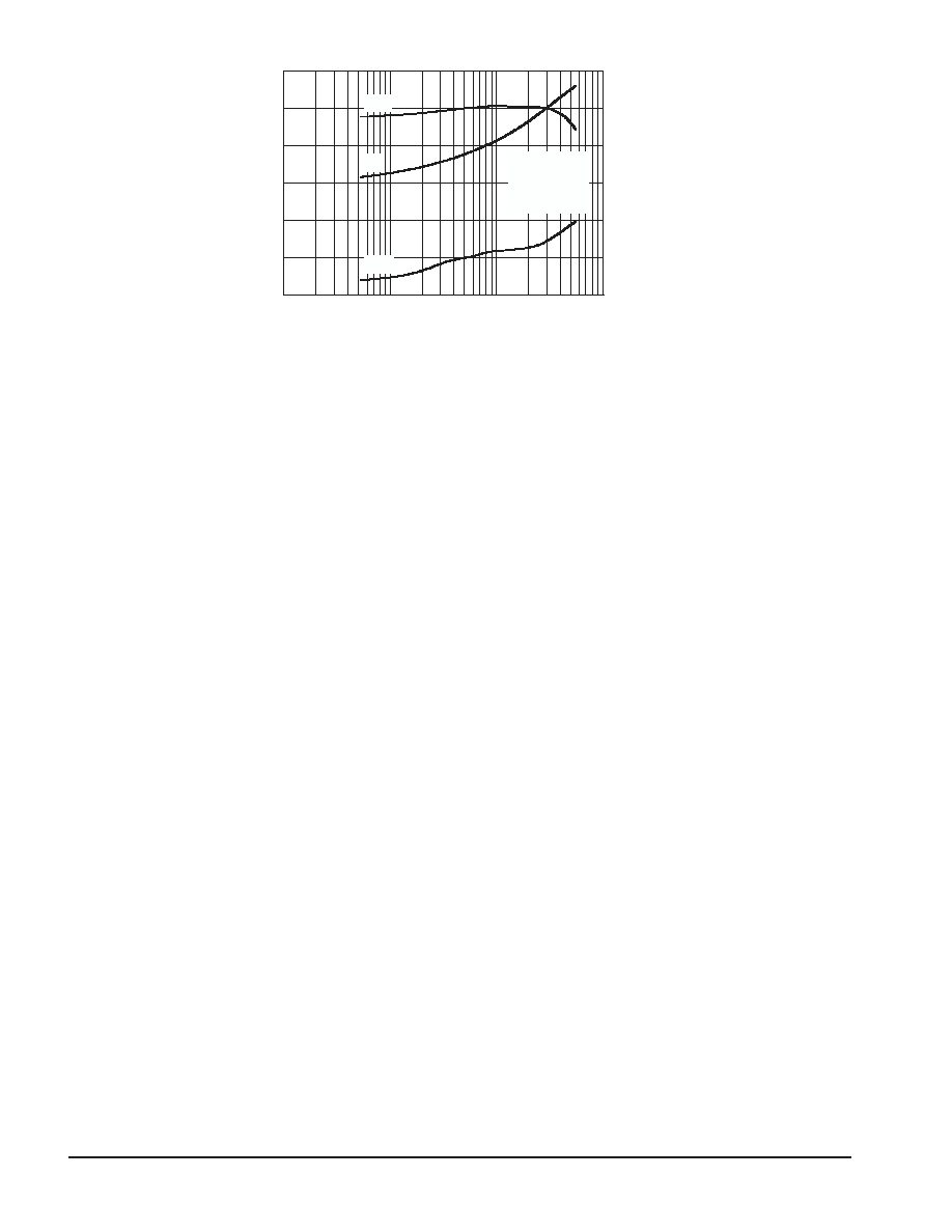
100
10
22
0.1
-60
60
G
ps
IMD
P
out
, OUTPUT POWER (WATTS) PEP
Figure 9. Power Gain, Efficiency and IMD
versus Output Power
G
ps
, POWER GAIN (dB)
INTERMODULA
TION DIST
ORTION (dBc)
IMD,
, DRAIN EFFICIENCY
(%)
V
DD
= 26 Vdc
I
DQ
= 250 mA
f1 = 945 MHz
f2 = 945.1 MHz
20
40
18
20
16
0
14
-20
12
-40
10
1
F
r
e
e
s
c
a
l
e
S
e
m
i
c
o
n
d
u
c
t
o
r
,
I
Freescale Semiconductor, Inc.
For More Information On This Product,
Go to: www.freescale.com
n
c
.
.
.
7
MRF9030MR1 MRF9030MBR1
MOTOROLA RF DEVICE DATA
f
MHz
Z
source
Z
load
930
945
960
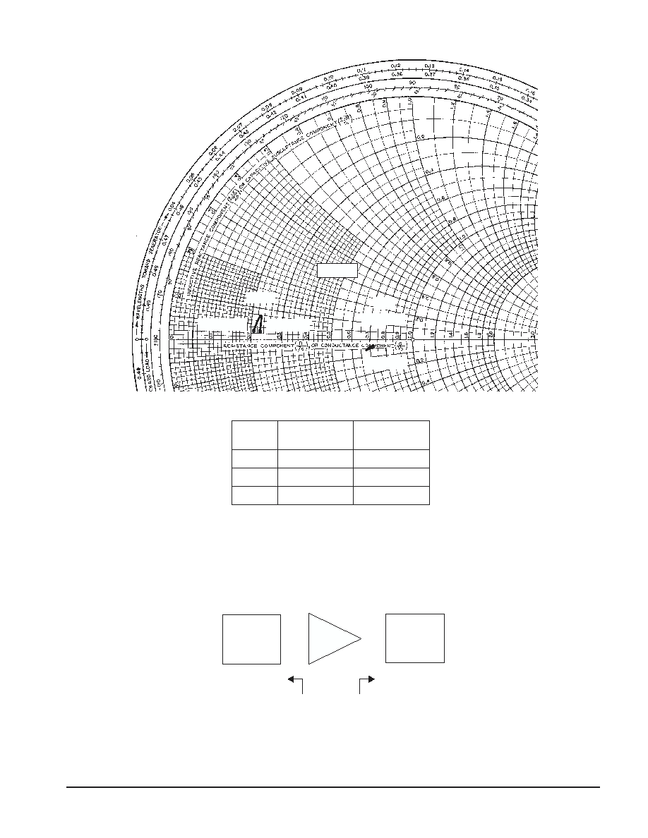
1.07 + j0.160
1.17 + j0.170
1.14 + j0.385
3.53 - j0.20
3.41 - j0.24
3.60 - j0.17
Z
source
= Test circuit impedance as measured from
gate to ground.
Z
load
= Test circuit impedance as measured
from drain to ground.
V
DD
= 26 V, I
DQ
= 250 mA, P
out
= 30 Watts (PEP)
Note: Z
load
was chosen based on tradeoffs between gain, output
power, drain efficiency and intermodulation distortion.
Figure 10. Series Equivalent Input and Output Impedance (MRF9030MR1)
f = 930 MHz
f = 930 MHz
f = 960 MHz
Z
o
= 5
f = 960 MHz
Zsource
Z load
Input
Matching
Network
Device
Under
Test
Output
Matching
Network
Z
source
Z
load
F
r
e
e
s
c
a
l
e
S
e
m
i
c
o
n
d
u
c
t
o
r
,
I
Freescale Semiconductor, Inc.
For More Information On This Product,
Go to: www.freescale.com
n
c
.
.
.
MRF9030MR1 MRF9030MBR1
8
MOTOROLA RF DEVICE DATA
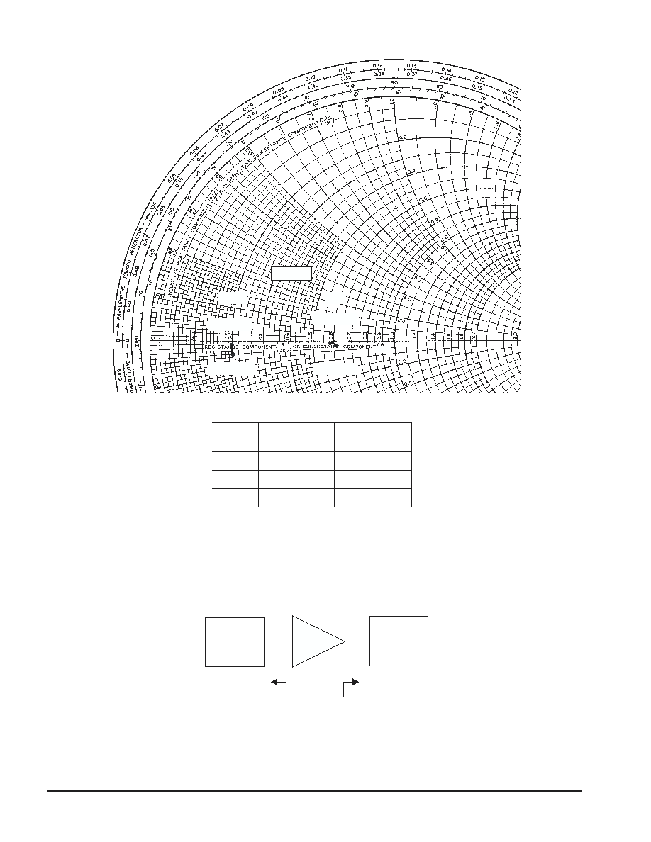
f
MHz
Z
source
Z
load
930
945
960
1.0 - j0.18
1.0 - j0.03
1.0 - j0.10
3.05 - j0.09
3.00 - j0.07
2.95 - j0.03
V
DD
= 26 V, I
DQ
= 250 mA, P
out
= 30 Watts (PEP)
Note: Z
load
was chosen based on tradeoffs between gain, output
power, drain efficiency and intermodulation distortion.
Figure 11. Series Equivalent Input and Output Impedance (MRF9030MBR1)
f = 930 MHz
Z
o
= 5
f = 960 MHz
f = 930 MHz
f = 960 MHz
Z
load
Z
source
= Test circuit impedance as measured from
gate to ground.
Z
load
= Test circuit impedance as measured
from drain to ground.
Zsource
Z load
Input
Matching
Network
Device
Under
Test
Output
Matching
Network
Z
source
F
r
e
e
s
c
a
l
e
S
e
m
i
c
o
n
d
u
c
t
o
r
,
I
Freescale Semiconductor, Inc.
For More Information On This Product,
Go to: www.freescale.com
n
c
.
.
.

9
MRF9030MR1 MRF9030MBR1
MOTOROLA RF DEVICE DATA
NOTES
F
r
e
e
s
c
a
l
e
S
e
m
i
c
o
n
d
u
c
t
o
r
,
I
Freescale Semiconductor, Inc.
For More Information On This Product,
Go to: www.freescale.com
n
c
.
.
.
MRF9030MR1 MRF9030MBR1
10
MOTOROLA RF DEVICE DATA
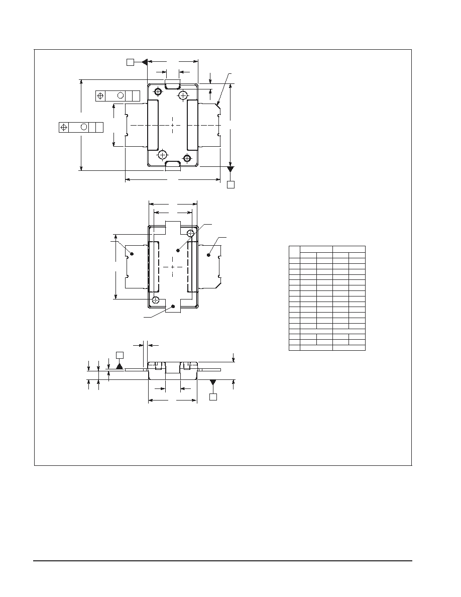
PACKAGE DIMENSIONS
TO-270-2
PLASTIC
MRF9030MR1
CASE 1265-08
ISSUE G
DATUM
PLANE
BOTTOM VIEW
A1
2X
E
D1
E4
E1
D2
E3
A2
EXPOSED
HEATSINK AREA
A
B
D
H
PIN ONE ID
««««
««««
««««
««««
««««
««««
««««
««««
D
A
M
aaa
D
A
M
aaa
D
2X
b1
2X
D3
NOTES:
1. CONTROLLING DIMENSION: INCH.
2. INTERPRET DIMENSIONS AND TOLERANCES
PER ASME Y14.5M-1994.
3. DATUM PLANE -H- IS LOCATED AT TOP OF LEAD
AND IS COINCIDENT WITH THE LEAD WHERE
THE LEAD EXITS THE PLASTIC BODY AT THE
TOP OF THE PARTING LINE.
4. DIMENSIONS "D1" AND "E1" DO NOT INCLUDE
MOLD PROTRUSION. ALLOWABLE PROTRUSION
IS .006 PER SIDE. DIMENSIONS "D1" AND "E1" DO
INCLUDE MOLD MISMATCH AND ARE DETER
MINED AT DATUM PLANE -H-.
5. DIMENSION b1 DOES NOT INCLUDE DAMBAR
PROTRUSION. ALLOWABLE DAMBAR
PROTRUSION SHALL BE .005 TOTAL IN EXCESS
OF THE b1 DIMENSION AT MAXIMUM MATERIAL
CONDITION.
6. DATUMS -A- AND -B- TO BE DETERMINED AT
DATUM PLANE -H-.
7. DIMENSION A2 APPLIES WITHIN ZONE "J" ONLY.
8. DIMENSIONS "D" AND "E2" DO NOT INCLUDE
MOLD PROTRUSION. ALLOWABLE PROTRUSION
IS .003 PER SIDE. DIMENSIONS "D" AND "E2" DO
INCLUDE MOLD MISMATCH AND ARE DETER
MINED AT DATUM PLANE -D-.
NOTE 7
c1
F
ZONE J
E2
2X
A
DIM
A
MIN
MAX
MIN
MAX
MILLIMETERS
.078
.082
1.98
2.08
INCHES
A1
.039
.043
0.99
1.09
A2
.040
.042
1.02
1.07
D
.416
.424
10.57
10.77
D1
.378
.382
9.60
9.70
D2
.290
.320
7.37
8.13
D3
.016
.024
0.41
0.61
E
.436
.444
11.07
11.28
E1
.238
.242
6.04
6.15
E2
.066
.074
1.68
1.88
E3
.150
.180
3.81
4.57
E4
.058
.066
1.47
1.68
F
b1
.193
.199
4.90
5.06
c1
.007
.011
0.18
0.28
aaa
.025 BSC
.004
0.64 BSC
0.10
PIN 1
PIN 2
PIN 3
STYLE 1:
PIN 1. DRAIN
2. GATE
3. SOURCE
E5
E5
E5
.231
.235
5.87
5.97
F
r
e
e
s
c
a
l
e
S
e
m
i
c
o
n
d
u
c
t
o
r
,
I
Freescale Semiconductor, Inc.
For More Information On This Product,
Go to: www.freescale.com
n
c
.
.
.
11
MRF9030MR1 MRF9030MBR1
MOTOROLA RF DEVICE DATA
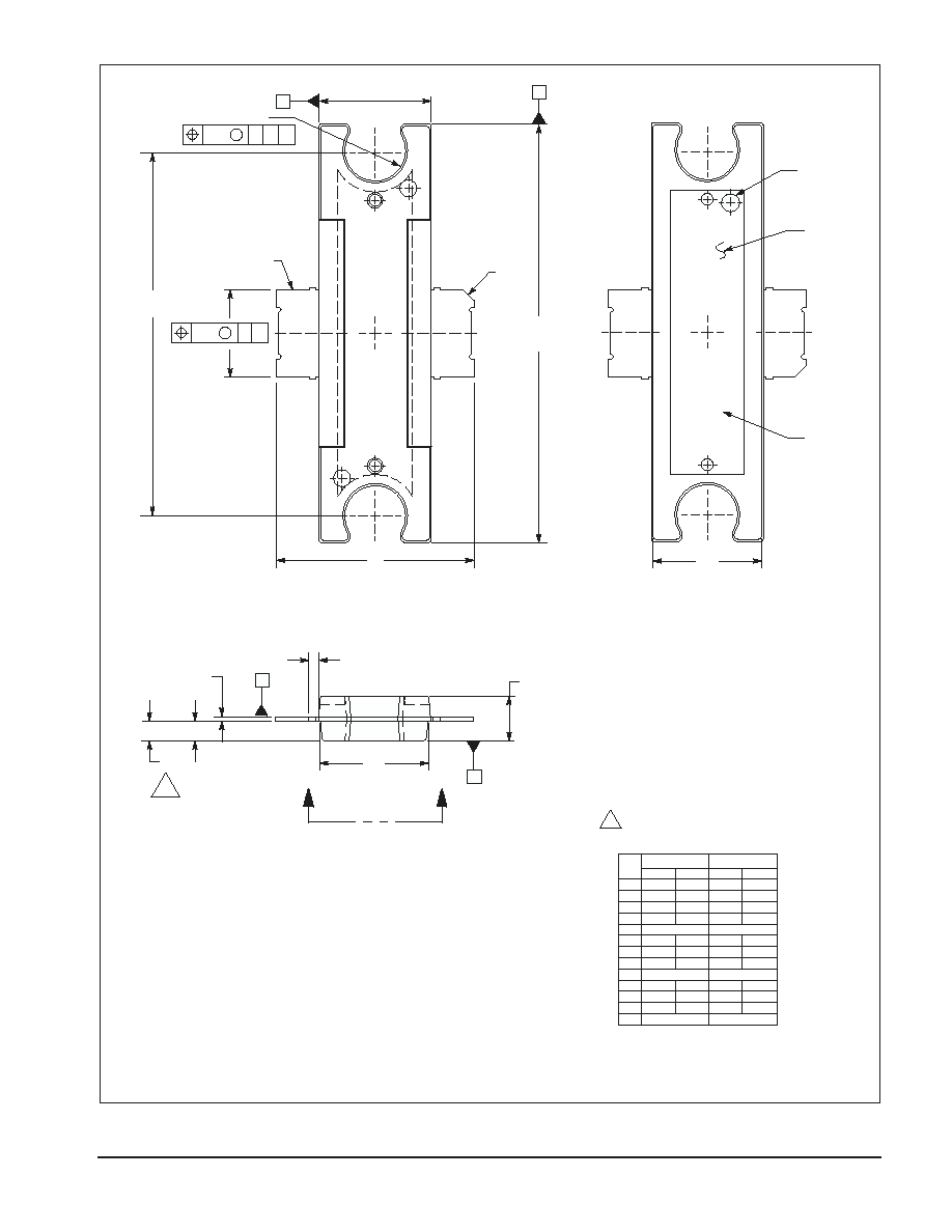
TO-272-2
PLASTIC
MRF9030MBR1
…………
…………
…………
…………
…………
…………
…………
…………
…………
…………
…………
…………
…………
CASE 1337-03
ISSUE B
NOTES:
1. CONTROLLING DIMENSION: INCH.
2. INTERPRET DIMENSIONS AND TOLERANCES
PER ASME Y14.5M, 1994.
3. DATUM PLANE -H- IS LOCATED AT THE TOP OF
LEAD AND IS COINCIDENT WITH THE LEAD
WHERE THE LEAD EXITS THE PLASTIC BODY AT
THE TOP OF THE PARTING LINE.
4. DIMENSIONS "D" AND "E1" DO NOT INCLUDE
MOLD PROTRUSION. ALLOWABLE PROTRUSION
IS .006 PER SIDE. DIMENSIONS "D" AND "E1" DO
INCLUDE MOLD MISMATCH AND ARE
DETERMINED AT DATUM PLANE -H-.
5. DIMENSION "b1" DOES NOT INCLUDE DAMBAR
PROTRUSION. ALLOWABLE DAMBAR
PROTRUSION SHALL BE .005 TOTAL IN EXCESS
OF THE "b1" DIMENSION AT MAXIMUM MATERIAL
CONDITION.
6. DATUMS -A- AND -B- TO BE DETERMINED AT
DATUM PLANE -H-.
7. DIMENSION A2 APPLIES WITHIN ZONE "J" ONLY.
8. CROSSHATCHING REPRESENTS THE EXPOSED
AREA OF THE HEAT SLUG.
H
C
A
B
SEATING
PLANE
DATUM
PLANE
2X
b1
A
E1
r1
DRAIN
LEAD
D
D1
E
NOTE 8
Y
Y
DIM
A
MIN
MAX
MIN
MAX
MILLIMETERS
.100
.104
2.54
2.64
INCHES
A1
.039
.043
0.99
1.09
A2
.040
.042
1.02
1.07
D
.928
.932
23.57
23.67
D1
E
.438
.442
11.12
11.23
E1
.248
.252
6.30
6.40
F
b1
.193
c1
.007
.011
.18
r1
.063
.068
1.60
aaa
1
VIEW Y-Y
.810 BSC
.004
20.57 BSC
.10
STYLE 1:
PIN 1. DRAIN
2. GATE
3. SOURCE
.025 BSC
.28
1.73
PIN 3
A1
A2
F
ZONE "J"
7
B
aaa
M
C A
aaa
M
C A
2X
.199
4.90
0.64 BSC
5.05
c1
2
DRAIN ID
GATE
LEAD
E2
E2
E2
.241
.245
6.12
6.22
F
r
e
e
s
c
a
l
e
S
e
m
i
c
o
n
d
u
c
t
o
r
,
I
Freescale Semiconductor, Inc.
For More Information On This Product,
Go to: www.freescale.com
n
c
.
.
.

MRF9030MR1 MRF9030MBR1
12
MOTOROLA RF DEVICE DATA
Information in this document is provided solely to enable system and software implementers to use Motorola products. There are no express or implied copyright
licenses granted hereunder to design or fabricate any integrated circuits or integrated circuits based on the information in this document.
Motorola reserves the right to make changes without further notice to any products herein. Motorola makes no warranty, representation or guarantee regarding
the suitability of its products for any particular purpose, nor does Motorola assume any liability arising out of the application or use of any product or circuit, and
specifically disclaims any and all liability, including without limitation consequential or incidental damages. "Typical" parameters that may be provided in Motorola
data sheets and/or specifications can and do vary in different applications and actual performance may vary over time. All operating parameters, including
"Typicals", must be validated for each customer application by customer's technical experts. Motorola does not convey any license under its patent rights nor the
rights of others. Motorola products are not designed, intended, or authorized for use as components in systems intended for surgical implant into the body, or other
applications intended to support or sustain life, or for any other application in which the failure of the Motorola product could create a situation where personal injury
or death may occur. Should Buyer purchase or use Motorola products for any such unintended or unauthorized application, Buyer shall indemnify and hold Motorola
and its officers, employees, subsidiaries, affiliates, and distributors harmless against all claims, costs, damages, and expenses, and reasonable attorney fees
arising out of, directly or indirectly, any claim of personal injury or death associated with such unintended or unauthorized use, even if such claim alleges that
Motorola was negligent regarding the design or manufacture of the part.
MOTOROLA and the Stylized M Logo are registered in the US Patent and Trademark Office. All other product or service names are the property of their respective
owners. Motorola, Inc. is an Equal Opportunity/Affirmative Action Employer.
E Motorola Inc. 2003
HOW TO REACH US:
USA/EUROPE/LOCATIONS NOT LISTED:
JAPAN: Motorola Japan Ltd.; SPS, Technical Information Center,
Motorola Literature Distribution
3-20-1, Minami-Azabu, Minato-ku, Tokyo 106-8573, Japan
P.O. Box 5405, Denver, Colorado 80217
81-3-3440-3569
1-800-521-6274 or 480-768-2130
ASIA/PACIFIC: Motorola Semiconductors H.K. Ltd.; Silicon Harbour Centre,
2 Dai King Street, Tai Po Industrial Estate, Tai Po, N.T., Hong Kong
852-26668334
HOME PAGE: http://motorola.com/semiconductors
MRF9030M/D
F
r
e
e
s
c
a
l
e
S
e
m
i
c
o
n
d
u
c
t
o
r
,
I
Freescale Semiconductor, Inc.
For More Information On This Product,
Go to: www.freescale.com
n
c
.
.
.