MRFG35003NT1 MRFG35003MT1 BWA
1
RF Reference Design Data
Freescale Semiconductor
RF Reference Design Library
Gallium Arsenide PHEMT
RF Power Field Effect Transistors
Device Characteristics (From Device Data Sheet)
Designed for WLL/MMDS/BWA or UMTS driver applications with frequencies
from 1.8 to 3.6 GHz. Devices are unmatched and are suitable for use in Class
AB linear base station applications.
∑ Typical W-CDMA Performance: -42 dBc ACPR, 3.55 GHz, 12 Volts,
I
DQ
= 55 mA, 5 MHz Offset/3.84 MHz BW, 64 DPCH (8.5 dB P/A
@ 0.01% Probability)
Output Power -- 300 mWatt
Power Gain -- 11.5 dB
Efficiency -- 25%
∑ 3 Watts P1dB @ 3.55 GHz
∑ Excellent Phase Linearity and Group Delay Characteristics
∑ High Gain, High Efficiency and High Linearity
∑ N Suffix Indicates Lead-Free Terminations
Reference Design Characteristics
∑ Typical Single-Channel W-CDMA Performance: -45 dBc ACPR,
2.45 GHz, 12 Volts, I
DQ
= 55 mA, 5 MHz Offset/3.84 MHz BW, 64 DPCH
(8.5 dB P/A @ 0.01% Probability)
Output Power -- 350 mWatt
Power Gain -- 12.5 dB
Efficiency -- 26%
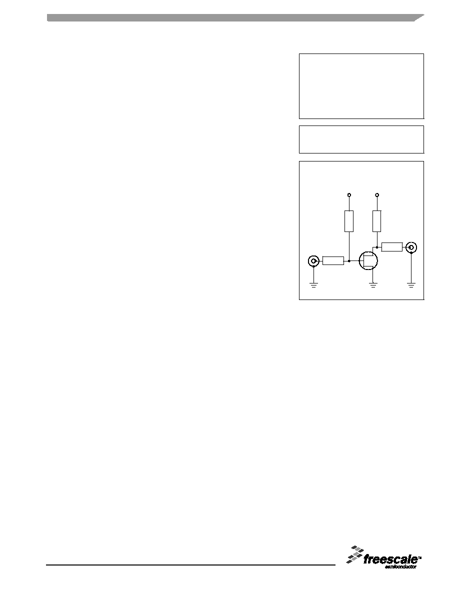
MRFG35003NT1(MT1) BWA 2.4-2.5 GHz REFERENCE DESIGN
Designed by: Monte Miller and Rick Hooper
This reference design is designed to demonstrate the typi-
cal RF performance characteristics of the
MRFG35003NT1(MT1) when applied for the 2.4-2.5 GHz
W-CDMA frequency band. The reference design is tuned for
the best tradeoff between good W-CDMA linearity and good
power capability and efficiency.
REFERENCE DESIGN LIBRARY TERMS
AND CONDITIONS
Freescale is pleased to make this reference design
available for your use in development and testing of your
own product or products, without charge. The reference
design contains easy - to - copy, fully functional amplifier
designs. Where possible, it consists of "no tune" distrib-
uted element matching circuits designed to be as small as
possible, includes temperature compensated bias circuit-
ry, and is designed to be used as "building blocks" for our
customers.
HEATSINKING
When operating this fixture please provide adequate heat-
sinking for the device. Excessive heating of the device will
prevent repeating of the included measurements.
NONLINEAR SIMULATION
To aid the design process and help reduce time to market
for our customers, Freescale provides device models for
several commercially available harmonic balance simulators.
Our model Library is available for all major computer platforms
supported by these simulators. For details on the RF model
library and supported harmonic balance simulators, go to the
following url:
http://www.freescale.com/rf/models
Available at http://www.freescale.com/rf, Go to Tool
s
Rev. 1, 6/2005
Freescale Semiconductor
Technical Data
MRFG35003NT1
MRFG35003MT1
BWA
BWA
2.4-2.5 GHz
RF
OUTPUT
RF
INPUT
MATC
H
MATC
H
BIAS
V
DD
V
GG
BIAS
Motorola, Inc. 2003
Freescale Semiconductor, Inc., 2005. All rights reserved.
2
RF Reference Design Data
Freescale Semiconductor
MRFG35003NT1 MRFG35003MT1 BWA
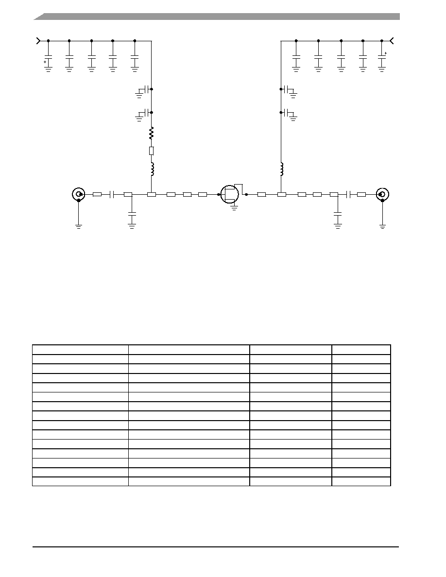
Figure 1. MRFG35003NT1(MT1) BWA Reference Design Schematic
Z7
0.045 x 0.100 Microstrip
Z9
0.200 x 0.040 Microstrip
Z10
0.260 x 0.020 Microstrip
Z11
0.200 x 0.516 Microstrip
Z12
0.044 x 0.534 Microstrip
PCB
Rogers 4350, 0.020,
r
= 3.50
Z1, Z13
0.044 x 0.295 Microstrip
Z2
0.044 x 0.730 Microstrip
Z3
0.105 x 0.045 Microstrip
Z4
0.044 x 0.015 Microstrip
Z5
0.340 x 0.320 Microstrip
Z6, Z8
0.146 x 0.070 Microstrip
C9
RF
INPUT
RF
OUTPUT
R1
C8
C7
C6
C5
C14
C13
C12
C11
C10
C4
C15
Z7
L2
C17
C2
C1
C18
Z1
Z2
Z3
Z8
Z10
Z9
Z11
Z12
Z13
V
DD
V
GS
Z6
Z4
Z5
L1
C3
C16
Table 1. MRFG35003NT1(MT1) BWA Reference Design Component Designations and Values
Part
Description
Value, P/N or DWG
Manufacturer
C1
3.9 pF Chip Capacitor
08051J3R9BBT
AVX
C2
0.9 pF Chip Capacitor
08051J0R9BBT
AVX
C3, C16
10 pF Chip Capacitors
100A100JP150X
ATC
C4, C15
100 pF Chip Capacitors
100A101JP150X
ATC
C5, C14
100 pF Chip Capacitors
100B101JP500X
ATC
C6, C13
1000 pF Chip Capacitors
100B102JP500X
ATC
C7, C12
0.1 µF Chip Capacitors
CDR33BX104AKWS
Kemet
C8, C11
39K pF Chip Capacitors
200B393KP500X
ATC
C9, C10
22 µF Tantalum Capacitors
T491X226K035AS
Newark
C17
1.0 pF Chip Capacitor
08051J1R0BBT
AVX
C18
15.0 pF Chip Capacitor
08051J15R0GBT
AVX
L1
4.7 nH Chip Inductor
LL2102-F4N7K
TOKO
L2
8.2 nH Chip Inductor
LL1608-FHN2K
TOKO
R1
75 W, 1/4 W 1% Chip Resistor
D55342M07B75JOR
Newark
MRFG35003NT1 MRFG35003MT1 BWA
3
RF Reference Design Data
Freescale Semiconductor
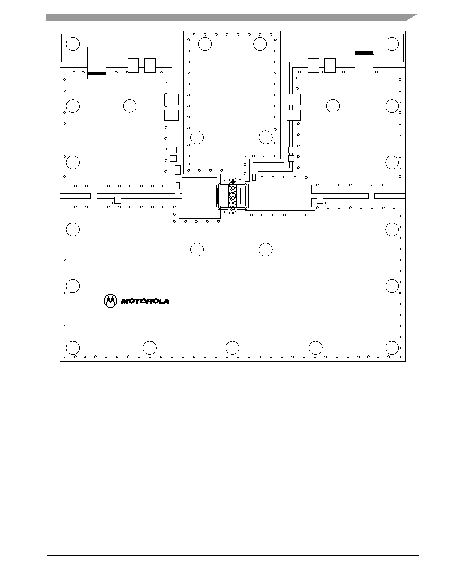
Figure 2. MRFG35003NT1(MT1) BWA Reference Design Component Layout
Rev 1
MRFG35003M
C16
C14
C15
C13
C12
C11
C10
C18
C1
C2
C17
C3
C5
C4
C6
C8
C7
C9
R1
L1
L2
Freescale has begun the transition of marking Printed Circuit Boards (PCBs) with the Freescale
Semiconductor signature/logo. PCBs may have either Motorola or Freescale markings during the
transition period. These changes will have no impact on form, fit or function of the current product.
4
RF Reference Design Data
Freescale Semiconductor
MRFG35003NT1 MRFG35003MT1 BWA
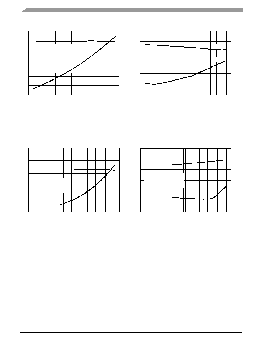
CHARACTERISTICS
1
4
18
0.1
10
45
P
out
, OUTPUT POWER (WATTS)
Figure 3. Transducer Gain and Power Added
Efficiency versus Output Power
G
T,
TRANSDUCER GAIN (dB)
P
AE, POWER
ADDED
EFFICIENCY
(%)
G
T
PAE
MRFG35003M @ 2.5 GHz
V
DS
= 12 Vdc, I
DQ
= 55 mA
f = 2.5 GHz, 8.5 P/A 3GPP W-CDMA
S
= 0.857È-136.97_
L
= 0.681È-178.94_
16
40
14
35
12
30
10
25
8
20
6
15
1
-60
0
0.1
-60
0
IRL
ACPR
P
out
, OUTPUT POWER (WATTS)
Figure 4. W-CDMA ACPR and Input Return
Loss versus Output Power
IRL,
INPUT
RETURN LOSS (dB)
ACPR, (dBc)
MRFG35003M @ 2.5 GHz
V
DS
= 12 Vdc, I
DQ
= 55 mA
f = 2.5 GHz, 8.5 P/A 3GPP W-CDMA
S
= 0.857È-136.97_,
L
= 0.681È-178.94_
-10
-10
-20
-20
-30
-30
-40
-40
-50
-50
NOTE: Data in Figures 3 and 4 is generated from load pull, not from the test circuit shown.
NOTE: Data in Figures 5 and 6 is generated from the test circuit shown.
1
6
16
0.01
0
50
G
T
PAE
P
out
, OUTPUT POWER (WATTS)
Figure 5. Transducer Gain and Power Added
Efficiency versus Output Power
G
T
,
TRANSDUCER GAIN (dB)
P
AE, POWER
ADDED
EFFICIENCY
(%)
MRFG35003M @ 2.45 GHz
V
DS
= 12 Vdc, I
DQ
= 55 mA
8.5 P/A 3GPP W-CDMA
0.1
14
40
12
30
10
20
8
10
1
-60
0
0.01
-60
0
IRL
ACPR
P
out
, OUTPUT POWER (WATTS)
Figure 6. W-CDMA ACPR and Input Return
Loss versus Output Power
IRL,
INPUT
RETURN LOSS (dB)
ACPR (dBc)
MRFG35003M @ 2.45 GHz
V
DS
= 12 Vdc, I
DQ
= 55 mA
8.5 P/A 3GPP W-CDMA
0.1
-10
-10
-20
-20
-30
-30
-40
-40
-50
-50

MRFG35003NT1 MRFG35003MT1 BWA
5
RF Reference Design Data
Freescale Semiconductor
Information in this document is provided solely to enable system and software
implementers to use Freescale Semiconductor products. There are no express or
implied copyright licenses granted hereunder to design or fabricate any integrated
circuits or integrated circuits based on the information in this document.
Freescale Semiconductor reserves the right to make changes without further notice to
any products herein. Freescale Semiconductor makes no warranty, representation or
guarantee regarding the suitability of its products for any particular purpose, nor does
Freescale Semiconductor assume any liability arising out of the application or use of
any product or circuit, and specifically disclaims any and all liability, including without
limitation consequential or incidental damages. "Typical" parameters that may be
provided in Freescale Semiconductor data sheets and/or specifications can and do
vary in different applications and actual performance may vary over time. All operating
parameters, including "Typicals", must be validated for each customer application by
customer's technical experts. Freescale Semiconductor does not convey any license
under its patent rights nor the rights of others. Freescale Semiconductor products are
not designed, intended, or authorized for use as components in systems intended for
surgical implant into the body, or other applications intended to support or sustain life,
or for any other application in which the failure of the Freescale Semiconductor product
could create a situation where personal injury or death may occur. Should Buyer
purchase or use Freescale Semiconductor products for any such unintended or
unauthorized application, Buyer shall indemnify and hold Freescale Semiconductor
and its officers, employees, subsidiaries, affiliates, and distributors harmless against all
claims, costs, damages, and expenses, and reasonable attorney fees arising out of,
directly or indirectly, any claim of personal injury or death associated with such
unintended or unauthorized use, even if such claim alleges that Freescale
Semiconductor was negligent regarding the design or manufacture of the part.
Freescalet and the Freescale logo are trademarks of Freescale Semiconductor, Inc.
All other product or service names are the property of their respective owners.
Freescale Semiconductor, Inc. 2005. All rights reserved.
How to Reach Us:
Home Page:
www.freescale.com
E-mail:
support@freescale.com
USA/Europe or Locations Not Listed:
Freescale Semiconductor
Technical Information Center, CH370
1300 N. Alma School Road
Chandler, Arizona 85224
+1-800-521-6274 or +1-480-768-2130
support@freescale.com
Europe, Middle East, and Africa:
Freescale Halbleiter Deutschland GmbH
Technical Information Center
Schatzbogen 7
81829 Muenchen, Germany
+44 1296 380 456 (English)
+46 8 52200080 (English)
+49 89 92103 559 (German)
+33 1 69 35 48 48 (French)
support@freescale.com
Japan:
Freescale Semiconductor Japan Ltd.
Headquarters
ARCO Tower 15F
1-8-1, Shimo-Meguro, Meguro-ku,
Tokyo 153-0064
Japan
0120 191014 or +81 3 5437 9125
support.japan@freescale.com
Asia/Pacific:
Freescale Semiconductor Hong Kong Ltd.
Technical Information Center
2 Dai King Street
Tai Po Industrial Estate
Tai Po, N.T., Hong Kong
+800 2666 8080
support.asia@freescale.com
For Literature Requests Only:
Freescale Semiconductor Literature Distribution Center
P.O. Box 5405
Denver, Colorado 80217
1-800-441-2447 or 303-675-2140
Fax: 303-675-2150
LDCForFreescaleSemiconductor@hibbertgroup.com
Available at http://www.freescale.com/rf, Go to Tool
s
Rev. 1, 6/2005