 | –≠–ª–µ–∫—Ç—Ä–æ–Ω–Ω—ã–π –∫–æ–º–ø–æ–Ω–µ–Ω—Ç: MRFG35010 | –°–∫–∞—á–∞—Ç—å:  PDF PDF  ZIP ZIP |
MRFG35010
5-1
Freescale Semiconductor
Wireless RF Product Device Data
Gallium Arsenide PHEMT
RF Power Field Effect Transistor
Designed for WLL/MMDS or UMTS driver applications with frequencies from
1.8 to 3.6 GHz. Device is unmatched and is suitable for use in Class AB or
Class A linear base station applications.
∑ Typical W-CDMA Performance: -42 dBc ACPR, 3.55 GHz, 12 Volts,
I
DQ
= 180 mA, 5 MHz Offset/3.84 MHz BW, 64 DPCH (8.5 dB P/A
@ 0.01% Probability)
Output Power -- 1 Watt
Power Gain -- 10 dB
Efficiency -- 30%
∑ 10 Watts P1dB @ 3.55 GHz
∑ Excellent Phase Linearity and Group Delay Characteristics
∑ High Gain, High Efficiency and High Linearity
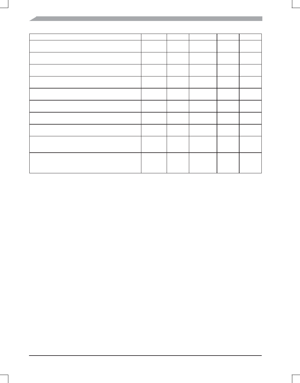
Table 1. Maximum Ratings
Rating
Symbol
Value
Unit
Drain-Source Voltage
V
DSS
15
Vdc
Total Device Dissipation @ T
C
= 25∞C
Derate above 25∞C
P
D
28.3
0.19
W
W/∞C
Gate-Source Voltage
V
GS
-5
Vdc
RF Input Power
P
in
33
dBm
Storage Temperature Range
T
stg
-65 to +175
∞C
Channel Temperature
(1)
T
ch
175
∞C
Operating Case Temperature Range
T
C
-20 to +90
∞C
Table 2. Thermal Characteristics
Characteristic
Symbol
Value
Unit
Thermal Resistance, Junction to Case
Class A
Class AB
R
JC
5.3
4.8
∞C/W
1. For reliable operation, the operating channel temperature should not exceed 150∞C.
MRFG35010
Rev. 6, 12/2004
Freescale Semiconductor
Technical Data
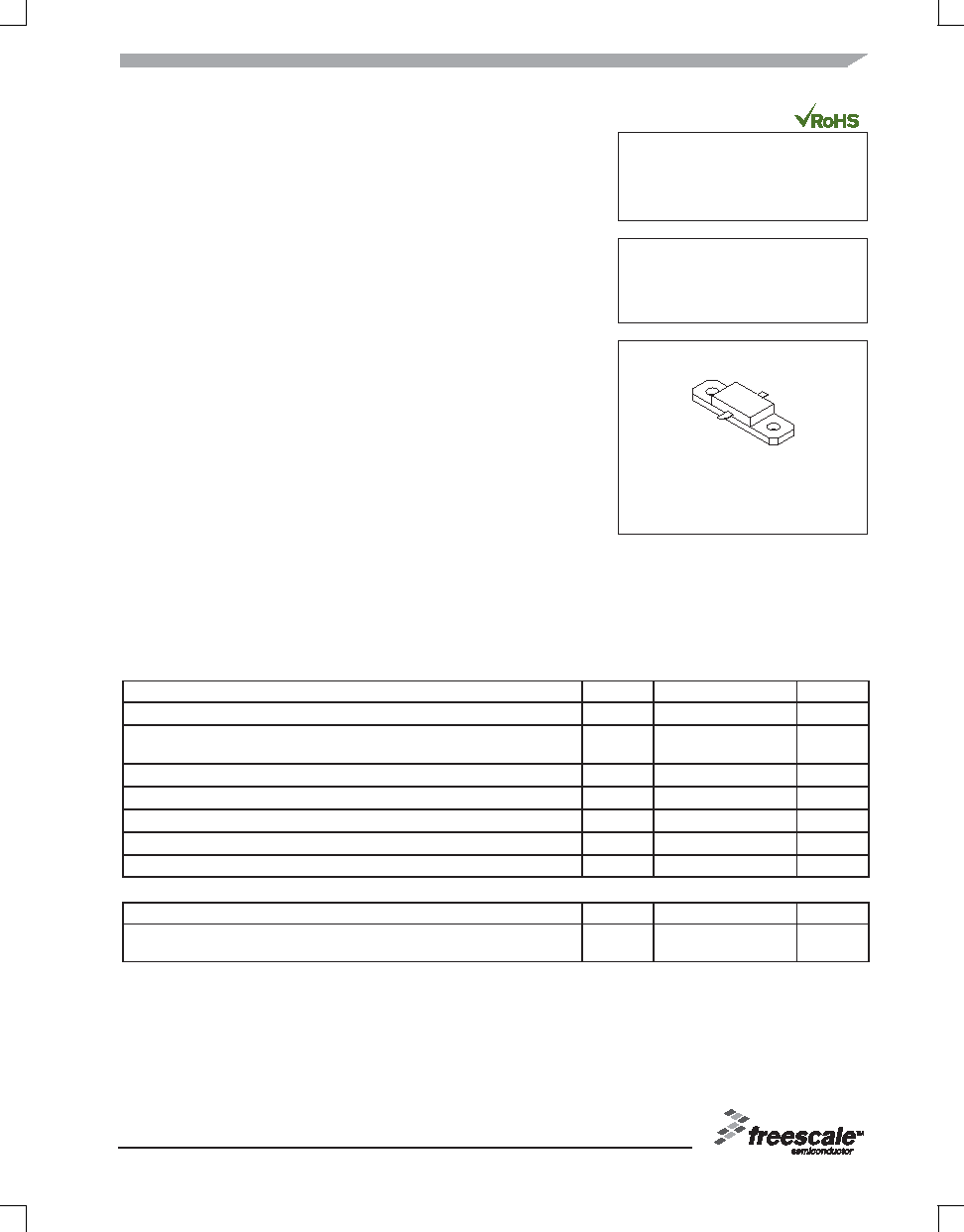
3.5 GHz, 10 W, 12 V
POWER FET
GaAs PHEMT
MRFG35010
CASE 360D-02, STYLE 1
NI-360HF
© Freescale Semiconductor, Inc., 2004. All rights reserved.
2
Freescale Semiconductor
Wireless RF Product Device Data
MRFG35010
Table 3. Electrical Characteristics
(T
C
= 25∞C unless otherwise noted)
Characteristic
Symbol
Min
Typ
Max
Unit
Saturated Drain Current
(V
DS
= 3.5 Vdc, V
GS
= 0 Vdc)
I
DSS
--
2.9
--
Adc
Off State Leakage Current
(V
GS
= -0.4 Vdc, V
DS
= 0 Vdc)
I
GSS
--
< 1.0
100
µAdc
Off State Drain Current
(V
DS
= 12 Vdc, V
GS
= -1.9 Vdc)
I
DSO
--
0.09
1.0
mAdc
Off State Current
(V
DS
= 28.5 Vdc, V
GS
= -2.5 Vdc)
I
DSX
--
5.0
15
mAdc
Gate-Source Cut-off Voltage
(V
DS
= 3.5 Vdc, I
DS
= 15 mA)
V
GS(th)
-1.2
-0.8
-0.7
Vdc
Quiescent Gate Voltage
(V
DS
= 12 Vdc, I
D
= 180 mA)
V
GS(Q)
-1.0
-0.8
-0.5
Vdc
Power Gain
(V
DD
= 12 Vdc, I
DQ
= 180 mA, f = 3.55 GHz)
G
ps
9.0
10
--
dB
Output Power, 1 dB Compression Point
(V
DD
= 12 Vdc, I
DQ
= 180 mA, f = 3.55 GHz)
P1dB
--
10
--
W
Drain Efficiency
(V
DD
= 12 Vdc, I
DQ
= 180 mA, P
out
= 1.0 W Avg.,
f = 3.55 GHz)
h
D
23
30
--
%
Adjacent Channel Power Ratio
(V
DD
= 12 Vdc, P
out
= 1.0 W Avg., I
DQ
= 180 mA,
f = 3.55 GHz, W-CDMA, 8.5 P/A @ 0.01% Probability,
64 CH, 3.84 MCPS)
ACPR
--
-42
-40
dBc
MRFG35010
3
Freescale Semiconductor
Wireless RF Product Device Data
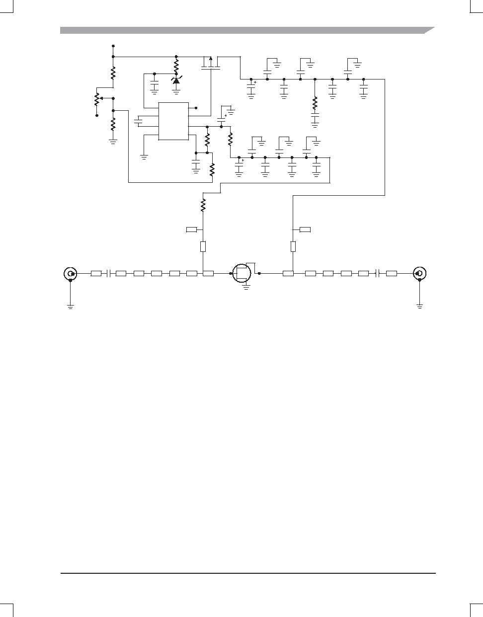
Figure 1. 3.4 - 3.6 GHz Single Supply Bias Sequencing Test Circuit Schematic
D1
C11
R3
R2
R1
C12
R7
C10
C9
C13
C15
C18
C14
C16
C19
R6
R4
R8
C1
Z1
C21
Q1
C7
C5
C3
C8
C6
C4
C2
U1
NC
RF
INPUT
RF
OUTPUT
V
DD
C17
R9
C20
1
2
3
4
8
7
6
5
C1, C21
6.8 pF Chip Capacitors, ATC
C2, C20
10 pF Chip Capacitors, ATC
C3, C19
100 pF Chip Capacitors, ATC
C4, C18
100 pF Chip Capacitors, ATC
C5, C10, C16, C17
1000 pF Chip Capacitors, ATC
C6, C11, C12, C15
0.1 µF Chip Capacitors, ATC
C7, C14
39K Chip Capacitors, ATC
C8, C13
22 µF Tantalum Chip Capacitors
C9
6.8 µF Tantalum Chip Capacitor
D1
5.1 V Zener Diode, MA8051CT-ND
R1
22.1 k, 1/4 W 1%, Chip Resistor
R2
5K Trim Pot, #3224W-1-502E
R3
12 k, 1/4 W 1%, Chip Resistor
R4
100 k, 1/4 W 1%, Chip Resistor
R5
39 k, 1/4 W 1%, Chip Resistor
R6
10 , 1/4 W 1%, Chip Resistor
R7
2.2 k, 1/4 W 1%, Chip Resistor
R8, R9
50 , 1/4 W 1%, Chip Resistors
U1
Voltage Converter, LTC 1261
Q1
Switch, MTP23P06V
PCB
Rogers RO4350, 0.020,
r
= 3.50
Z1
0.044 x 0.250 Microstrip
Z2
0.044 x 0.030 Microstrip
Z3
0.615 x 0.050 Microstrip
Z4
0.044 x 0.070 Microstrip
Z5
0.270 x 0.490 Microstrip
Z6
0.044 x 0.470 Microstrip
Z7
0.434 x 0.110 Microstrip
Z8, Z11
0.015 x 0.527 Microstrip
Z9, Z10
0.290 x 90∞ Microstrip Radial Stub
Z12
0.184 x 0.390 Microstrip
Z13
0.040 x 0.580 Microstrip
Z14
0.109 x 0.099 Microstrip
Z15
0.030 x 0.225 Microstrip
Z16
0.080 x 0.240 Microstrip
Z17
0.044 x 0.143 Microstrip
R5
Z2
Z3
Z4
Z5
Z6
Z7
Z12
Z13
Z14
Z15
Z16
Z17
Z9
Z10
Z8
Z11
4
Freescale Semiconductor
Wireless RF Product Device Data
MRFG35010
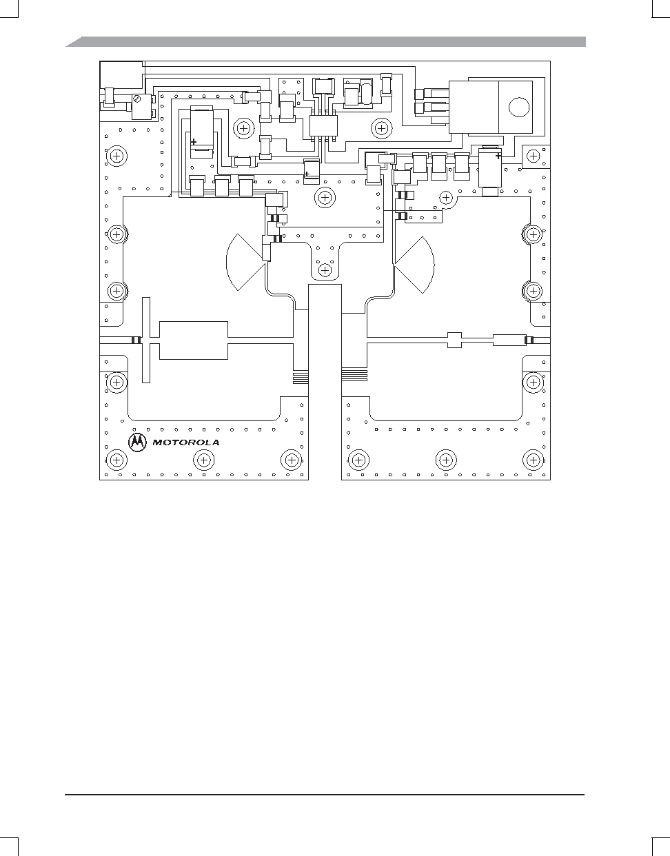
Figure 2. 3.4 - 3.6 GHz Test Circuit Component Layout
Rev-06
MRFG35010
V
DD
= 12 V
GND
CUT
OUT
AREA
OUTPUT
INPUT
Q1
C1
C2
C3
C4
C5
C6
C7
C8
C9
C10
C11
C12 D1
C13
C14
C15
C16
C17
C18
C19
C20
C21
R1
R2
R3 R4
R5
R6
R7
R9
R8
G
D
S
U1
Freescale has begun the transition of marking Printed Circuit Boards (PCBs) with the Freescale Semiconductor
signature/logo. PCBs may have either Motorola or Freescale markings during the transition period. These changes will have
no impact on form, fit or function of the current product.
MRFG35010
5
Freescale Semiconductor
Wireless RF Product Device Data
TYPICAL CHARACTERISTICS
NOTE: All data is referenced to package lead interface.
S
and
L
are the impedances presented to the DUT.
All data is generated from load pull, not from the test circuit shown.
1
9.5
13.5
13
12.5
12
11.5
11
10.5
10
10
0.1
0
80
G
ps
P
out
, OUTPUT POWER (WATTS)
Figure 3. Power Gain and Drain Efficiency
versus Output Power
G
ps
, POWER GAIN (dB)
, DRAIN EFFICIENCY
(%)
D
D
70
60
50
40
30
20
10
V
DS
= 12 Vdc, I
DQ
= 180 mA
f = 3.55 GHz, 8.5 dB P/A 3GPP W-CDMA
S
= 0.857È-144.24_,
L
= 0.798È-164.30_
10
-70
0
0.1
-70
0
IRL
ACPR
P
out
, OUTPUT POWER (WATTS)
Figure 4. W-CDMA ACPR and Input Return Loss
versus Output Power
ACPR (dBc)
INPUT
RETURN LOSS (dB)
IRL,
-10
-10
-20
-20
-30
-30
-40
-40
-50
-50
-60
-60
1
V
DS
= 12 Vdc, I
DQ
= 180 mA
f = 3.55 GHz, 8.5 dB P/A 3GPP W-CDMA
S
= 0.857È-144.24_,
L
= 0.798È-164.30_
25
36
5
0
60
P
out
V
DS
= 12 Vdc, I
DQ
= 180 mA
f = 3.55 GHz, 8.5 dB P/A 3GPP W-CDMA
S
= 0.857È-144.24_,
L
= 0.798È-164.30_
P
in
, INPUT POWER (dBm)
Figure 5. W-CDMA Output Power and Drain
Efficiency versus Input Power
34
32
45
30
28
30
26
24
15
22
20
10
15
20
P out
, OUTPUT
POWER (dBm)
, DRAIN EFFICIENCY
(%)
D
D
6
Freescale Semiconductor
Wireless RF Product Device Data
MRFG35010
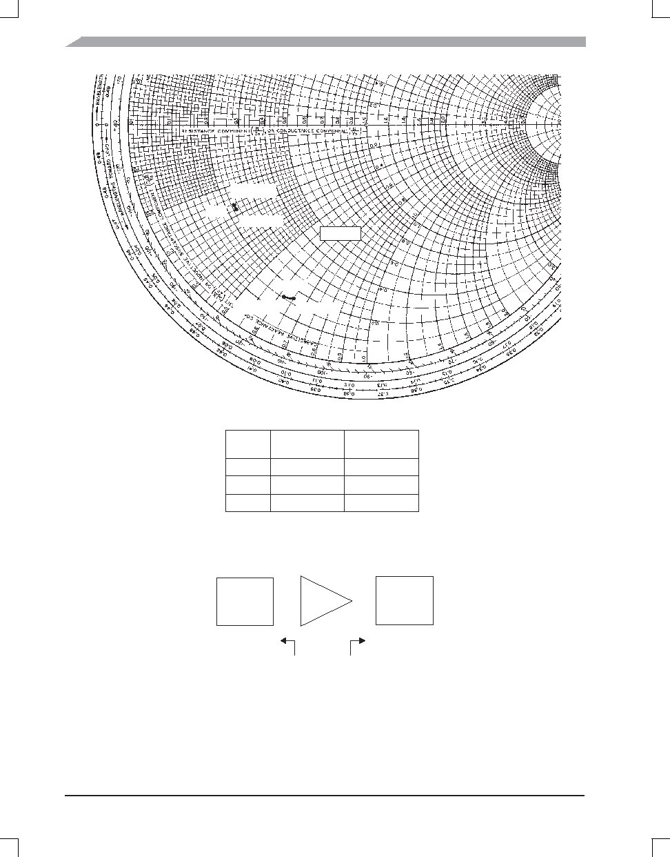
f
MHz
Z
source
Z
load
3500
3550
3600
4.3 - j16.3
4.1 - j15.8
4.2 - j16.0
5.7 - j7.0
5.7 - j6.8
5.7 - j6.6
V
DD
= 12 V, I
DQ
=180 mA, P
out
= 1 W
Figure 6. Series Equivalent Source and Load Impedance
Z
o
= 25
Z
load
f = 3500 MHz
f = 3600 MHz
f = 3500 MHz
f = 3600 MHz
Z
source
Z
source
= Test circuit impedance as measured from
gate to ground.
Z
load
= Test circuit impedance as measured
from drain to ground.
Z source
Z load
Input
Matching
Network
Device
Under
Test
Output
Matching
Network
MRFG35010
7
Freescale Semiconductor
Wireless RF Product Device Data
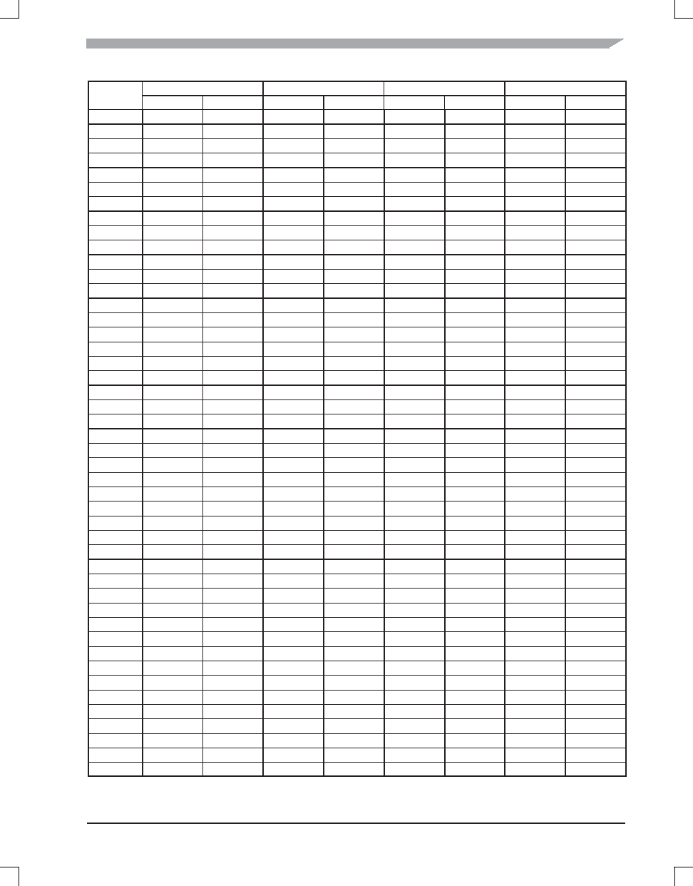
Table 4. Class A Common Source S-Parameters at V
DS
= 12 Vdc, I
DQ
= 1000 mA
f
S
11
S
21
S
12
S
22
f
GHz
|S
11
|
|S
21
|
|S
12
|
|S
22
|
0.50
0.956
-177.95
5.591
79.60
0.007
15.64
0.741
179.71
0.60
0.957
-179.86
4.668
76.30
0.007
23.81
0.739
179.15
0.70
0.956
178.44
4.007
73.21
0.008
23.84
0.736
178.75
0.80
0.956
177.05
3.520
70.18
0.008
26.09
0.736
178.29
0.90
0.954
175.83
3.138
67.20
0.009
30.55
0.735
177.85
1.00
0.955
174.61
2.842
64.30
0.010
28.91
0.735
177.42
1.10
0.954
173.42
2.604
61.65
0.009
31.64
0.734
176.95
1.20
0.952
172.29
2.402
58.87
0.011
31.90
0.735
176.52
1.30
0.952
171.25
2.236
56.13
0.011
36.06
0.735
175.97
1.40
0.950
170.02
2.098
53.34
0.011
33.99
0.736
175.52
1.50
0.950
168.36
2.054
50.41
0.011
32.65
0.725
174.86
1.60
0.948
167.24
1.944
47.63
0.012
32.47
0.725
174.31
1.70
0.946
166.01
1.850
44.77
0.013
37.07
0.725
173.70
1.80
0.944
164.67
1.769
42.06
0.014
34.40
0.725
172.90
1.90
0.943
163.59
1.698
39.29
0.015
35.71
0.725
172.32
2.00
0.942
162.31
1.638
36.53
0.015
37.47
0.724
171.58
2.10
0.940
161.09
1.580
33.69
0.016
35.82
0.724
170.75
2.20
0.938
159.66
1.532
30.84
0.017
35.69
0.722
169.89
2.30
0.937
158.30
1.491
28.03
0.017
35.43
0.721
169.04
2.40
0.935
156.86
1.454
25.19
0.019
34.19
0.720
168.15
2.50
0.934
155.35
1.422
22.38
0.020
34.10
0.718
167.32
2.60
0.932
153.83
1.396
19.54
0.021
35.51
0.718
166.38
2.70
0.928
152.26
1.375
16.68
0.022
33.15
0.716
165.61
2.80
0.926
150.58
1.356
13.80
0.023
30.84
0.714
164.67
2.90
0.923
148.97
1.342
10.91
0.025
31.00
0.711
163.77
3.00
0.920
147.18
1.332
7.87
0.027
29.11
0.708
162.89
3.10
0.917
145.27
1.328
4.88
0.028
28.98
0.704
161.96
3.20
0.913
143.23
1.326
1.73
0.030
27.36
0.699
161.08
3.30
0.908
141.12
1.329
-1.48
0.032
25.93
0.694
160.09
3.40
0.903
138.91
1.335
-4.80
0.034
24.33
0.687
159.09
3.50
0.897
136.46
1.346
-8.26
0.036
22.30
0.679
158.02
3.60
0.893
133.77
1.360
-11.89
0.039
19.80
0.670
156.93
3.70
0.884
130.86
1.375
-15.61
0.042
17.46
0.659
155.90
3.80
0.875
127.58
1.393
-19.50
0.045
15.22
0.648
154.96
3.90
0.866
124.06
1.417
-23.55
0.048
13.31
0.636
154.06
4.00
0.851
120.13
1.443
-27.75
0.052
10.27
0.626
153.16
4.10
0.833
115.98
1.472
-32.06
0.056
7.36
0.618
152.14
4.20
0.814
111.48
1.505
-36.63
0.060
4.18
0.609
151.13
4.30
0.793
106.69
1.541
-41.44
0.065
1.13
0.602
149.84
4.40
0.771
101.44
1.581
-46.57
0.071
-3.19
0.592
148.47
4.50
0.748
95.69
1.622
-51.82
0.076
-7.50
0.582
147.06
4.60
0.723
89.38
1.668
-57.33
0.082
-11.79
0.575
145.72
4.70
0.697
82.41
1.721
-63.32
0.089
-16.57
0.568
144.03
4.80
0.672
74.51
1.771
-69.70
0.096
-22.28
0.559
142.02
4.90
0.647
65.82
1.818
-76.56
0.103
-28.04
0.549
139.82
5.00
0.622
56.14
1.860
-83.67
0.110
-33.91
0.539
137.39
8
Freescale Semiconductor
Wireless RF Product Device Data
MRFG35010
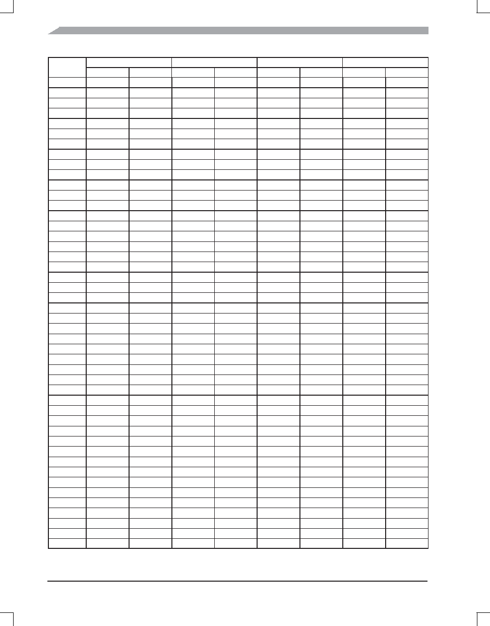
Table 5. Class AB Common Source S-Parameters at V
DS
= 12 Vdc, I
DQ
= 180 mA
f
S
11
S
21
S
12
S
22
f
GHz
|S
11
|
|S
21
|
|S
12
|
|S
22
|
0.50
0.936
-175.05
5.292
80.70
0.014
3.73
0.735
-178.66
0.60
0.936
-177.28
4.422
77.20
0.014
3.63
0.735
-179.61
0.70
0.935
-179.21
3.803
74.02
0.015
3.78
0.735
179.80
0.80
0.935
179.21
3.341
70.87
0.014
7.22
0.736
179.20
0.90
0.935
177.77
2.983
67.85
0.014
5.83
0.738
178.58
1.00
0.934
176.46
2.701
64.80
0.015
7.03
0.738
178.09
1.10
0.934
175.26
2.473
62.00
0.015
7.15
0.738
177.54
1.20
0.933
174.05
2.284
59.24
0.014
6.85
0.739
177.01
1.30
0.933
172.86
2.124
56.47
0.015
6.90
0.740
176.42
1.40
0.933
171.71
1.991
53.70
0.015
8.93
0.739
175.92
1.50
0.929
170.06
1.948
50.73
0.016
7.81
0.730
175.22
1.60
0.930
168.89
1.845
47.88
0.016
8.58
0.731
174.51
1.70
0.927
167.73
1.757
44.99
0.016
8.16
0.731
173.88
1.80
0.926
166.37
1.678
42.32
0.016
10.00
0.730
173.09
1.90
0.925
165.33
1.610
39.48
0.017
9.25
0.732
172.45
2.00
0.923
164.05
1.551
36.70
0.018
11.89
0.731
171.71
2.10
0.921
162.82
1.498
33.90
0.018
10.06
0.731
170.85
2.20
0.920
161.49
1.451
31.07
0.018
10.11
0.730
170.01
2.30
0.918
160.17
1.411
28.22
0.019
10.86
0.729
169.14
2.40
0.916
158.74
1.376
25.43
0.020
9.05
0.728
168.25
2.50
0.916
157.35
1.347
22.58
0.020
8.57
0.727
167.43
2.60
0.913
155.97
1.321
19.80
0.021
9.64
0.727
166.51
2.70
0.912
154.45
1.300
16.98
0.022
10.23
0.725
165.61
2.80
0.909
152.83
1.280
14.05
0.023
9.68
0.723
164.76
2.90
0.907
151.25
1.268
11.14
0.024
10.24
0.719
163.70
3.00
0.904
149.54
1.257
8.18
0.026
7.35
0.717
162.83
3.10
0.901
147.76
1.253
5.20
0.026
9.11
0.714
161.86
3.20
0.896
145.88
1.253
2.11
0.028
6.33
0.709
160.85
3.30
0.893
143.83
1.255
-1.10
0.030
7.09
0.704
159.82
3.40
0.887
141.78
1.260
-4.43
0.031
5.16
0.697
158.76
3.50
0.882
139.43
1.268
-7.81
0.033
4.74
0.690
157.60
3.60
0.876
136.99
1.281
-11.29
0.035
4.34
0.682
156.46
3.70
0.870
134.24
1.295
-14.96
0.038
1.64
0.672
155.26
3.80
0.863
131.29
1.311
-18.72
0.040
0.43
0.660
154.16
3.90
0.853
127.96
1.334
-22.68
0.042
-2.33
0.650
153.12
4.00
0.840
124.33
1.354
-26.85
0.046
-4.01
0.639
152.16
4.10
0.825
120.40
1.386
-31.01
0.049
-6.67
0.632
150.97
4.20
0.807
116.26
1.414
-35.40
0.053
-9.06
0.624
149.72
4.30
0.787
111.78
1.453
-40.01
0.057
-11.29
0.617
148.33
4.40
0.767
106.97
1.492
-44.83
0.061
-14.79
0.608
146.78
4.50
0.745
101.74
1.537
-49.99
0.066
-18.66
0.599
145.00
4.60
0.721
95.90
1.579
-55.50
0.071
-22.20
0.589
143.33
4.70
0.697
89.39
1.633
-61.25
0.077
-26.02
0.580
141.41
4.80
0.674
82.09
1.685
-67.46
0.084
-30.63
0.569
139.21
4.90
0.647
73.93
1.740
-74.01
0.090
-35.78
0.557
136.94
5.00
0.622
64.84
1.790
-81.02
0.097
-41.70
0.545
134.20

MRFG35010
9
Freescale Semiconductor
Wireless RF Product Device Data
NOTES

10
Freescale Semiconductor
Wireless RF Product Device Data
MRFG35010
NOTES

MRFG35010
11
Freescale Semiconductor
Wireless RF Product Device Data
PACKAGE DIMENSIONS
CASE 360D-02
ISSUE B
G
E
N (LID)
C
SEATING
PLANE
DIM
A
MIN
MAX
MIN
MAX
MILLIMETERS
.795
.805
20.19
20.45
INCHES
B
.225
.235
5.72
5.97
C
.125
.176
3.18
4.47
D
.034
.044
0.89
1.12
E
.055
.065
1.40
1.65
F
.004
.006
0.10
0.15
G
.562 BSC
14.28 BSC
H
.077
.087
1.96
2.21
K
.085
.115
2.16
2.92
M
.355
.365
9.02
9.27
N
.355
.365
9.96
10.16
STYLE 1:
PIN 1. GATE
2. DRAIN
3. SOURCE
1
2
3
Q
2 x
M
A
M
bbb
B
M
T
NOTES:
1. CONTROLLING DIMENSION: INCH.
2. INTERPRET DIMENSIONS AND TOLERANCES
PER ASME Y14.5M-1994.
3. DIMENSION H IS MEASURED .030 (0.762) AWAY
FROM PACKAGE BODY.
Q
.125
.135
3.18
3.43
R
.225
.235
5.72
5.97
S
.225
.235
5.72
5.97
aaa
bbb
ccc
.005
0.13
.010
0.25
.015
0.38
M
A
M
bbb
B
M
T
S
(INSULATOR)
K
2 x
B
(FLANGE)
D
2 x
M
A
M
bbb
B
M
T
B
M
A
M
ccc
B
M
T
H
R (LID)
F
M
A
M
ccc
B
M
T
T
A
A
M
M
A
M
aaa
B
M
T
(INSULATOR)
NI-360HF

5-12
Freescale Semiconductor
Wireless RF Product Device Data
MRFG35010
Information in this document is provided solely to enable system and software
implementers to use Freescale Semiconductor products. There are no express or
implied copyright licenses granted hereunder to design or fabricate any integrated
circuits or integrated circuits based on the information in this document.
Freescale Semiconductor reserves the right to make changes without further notice to
any products herein. Freescale Semiconductor makes no warranty, representation or
guarantee regarding the suitability of its products for any particular purpose, nor does
Freescale Semiconductor assume any liability arising out of the application or use of
any product or circuit, and specifically disclaims any and all liability, including without
limitation consequential or incidental damages. "Typical" parameters that may be
provided in Freescale Semiconductor data sheets and/or specifications can and do
vary in different applications and actual performance may vary over time. All operating
parameters, including "Typicals", must be validated for each customer application by
customer's technical experts. Freescale Semiconductor does not convey any license
under its patent rights nor the rights of others. Freescale Semiconductor products are
not designed, intended, or authorized for use as components in systems intended for
surgical implant into the body, or other applications intended to support or sustain life,
or for any other application in which the failure of the Freescale Semiconductor product
could create a situation where personal injury or death may occur. Should Buyer
purchase or use Freescale Semiconductor products for any such unintended or
unauthorized application, Buyer shall indemnify and hold Freescale Semiconductor
and its officers, employees, subsidiaries, affiliates, and distributors harmless against all
claims, costs, damages, and expenses, and reasonable attorney fees arising out of,
directly or indirectly, any claim of personal injury or death associated with such
unintended or unauthorized use, even if such claim alleges that Freescale
Semiconductor was negligent regarding the design or manufacture of the part.
Freescalet and the Freescale logo are trademarks of Freescale Semiconductor, Inc.
All other product or service names are the property of their respective owners.
© Freescale Semiconductor, Inc. 2004. All rights reserved.
How to Reach Us:
Home Page:
www.freescale.com
E-mail:
support@freescale.com
USA/Europe or Locations Not Listed:
Freescale Semiconductor
Technical Information Center, CH370
1300 N. Alma School Road
Chandler, Arizona 85224
+1-800-521-6274 or +1-480-768-2130
support@freescale.com
Europe, Middle East, and Africa:
Freescale Halbleiter Deutschland GmbH
Technical Information Center
Schatzbogen 7
81829 Muenchen, Germany
+44 1296 380 456 (English)
+46 8 52200080 (English)
+49 89 92103 559 (German)
+33 1 69 35 48 48 (French)
support@freescale.com
Japan:
Freescale Semiconductor Japan Ltd.
Headquarters
ARCO Tower 15F
1-8-1, Shimo-Meguro, Meguro-ku,
Tokyo 153-0064
Japan
0120 191014 or +81 3 5437 9125
support.japan@freescale.com
Asia/Pacific:
Freescale Semiconductor Hong Kong Ltd.
Technical Information Center
2 Dai King Street
Tai Po Industrial Estate
Tai Po, N.T., Hong Kong
+800 2666 8080
support.asia@freescale.com
For Literature Requests Only:
Freescale Semiconductor Literature Distribution Center
P.O. Box 5405
Denver, Colorado 80217
1-800-441-2447 or 303-675-2140
Fax: 303-675-2150
LDCForFreescaleSemiconductor@hibbertgroup.com
MRFG35010
Rev. 6, 12/2004
Document Number:
RoHS-compliant and/or Pb- free versions of Freescale products have the functionality
and electrical characteristics of their non-RoHS-compliant and/or non-Pb- free
counterparts. For further information, see http://www.freescale.com or contact your
Freescale sales representative.
For information on Freescale.s Environmental Products program, go to
http://www.freescale.com/epp.