 | –≠–ª–µ–∫—Ç—Ä–æ–Ω–Ω—ã–π –∫–æ–º–ø–æ–Ω–µ–Ω—Ç: MRFIC0970 | –°–∫–∞—á–∞—Ç—å:  PDF PDF  ZIP ZIP |
MRFIC0970
Ordering Information
Device
Marking
Package
MRFIC0970
0970
QFN-20
Package Information
Plastic Package
Case 1308
(QFN-20)
(Scale 2:1)
Definitive Data: Motorola reserves the right to change the Production detail specifications as may be required to
permit improvements in the design of its product. © Motorola, Inc., 2002. All rights reserved.
The MRFIC0970 is a single supply, RF power amplifier designed for the 2.0 W GSM900
handheld radios. The device is packaged in the QFN-20 package, with exposed backside pad,
which allows excellent electrical and thermal performance through a solderable contact.
∑
Target 3.2 V Characteristics:
RF Output Power: 34.5 dBm Typical
Efficiency: 50% Typical
∑
Single Positive Supply Solution
∑
Available in Tape and Reel only. R2 Suffix = 2500 Units per 12 mm, 13 inch Reel
Technical Data
MRFIC0970/D
Rev. 0, 07/2002
3.2 V GSM GaAs
Integrated Power
Amplifier
F
r
e
e
s
c
a
l
e
S
e
m
i
c
o
n
d
u
c
t
o
r
,
I
Freescale Semiconductor, Inc.
For More Information On This Product,
Go to: www.freescale.com
n
c
.
.
.
2
MRFIC0970 Technical Data
MOTOROLA
Electrical Characteristics
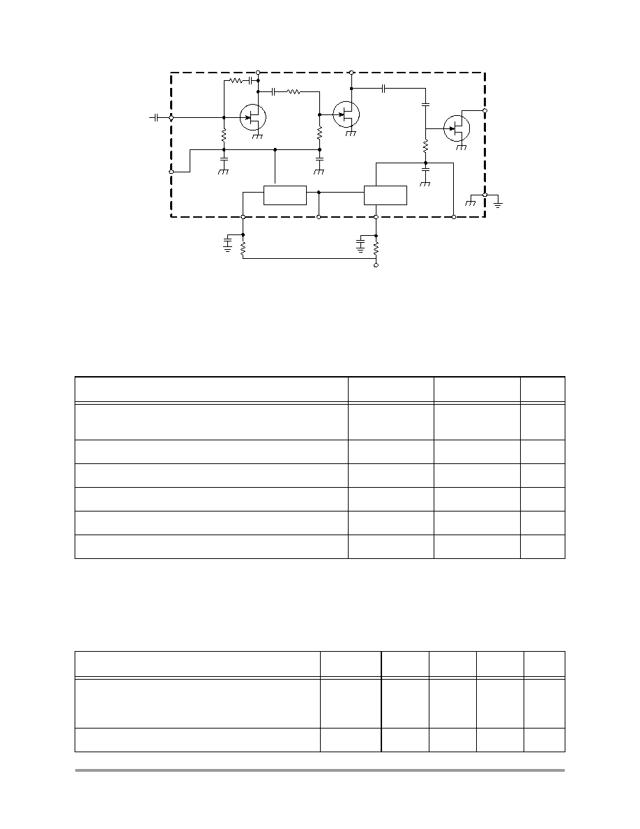
Figure 1. Functional Block Diagram
1 Electrical Characteristics
Table 1. Maximum Ratings
Rating
Symbol
Value
Unit
Supply Voltage
V
D1,2,3
, V
abc
V
ref
8.0
5.0
V
V
RF Input Power
P
in
15
dBm
RF Output Power
P
out
38
dBm
Operating Case Temperature Range
T
C
-40 to 85
∞
C
Storage Temperature Range
T
stg
-40 to 85
∞
C
Junction Temperature
T
J
150
∞
C
NOTES: 1. Maximum Ratings are those values beyond which damage to the device may occur.
Functional operation should be restricted to the limits in the Electrical Characteristics
or Recommended Operating Conditions tables.
2 ESD (electrostatic discharge) immunity meets Human Body Model (HBM)
250 V and
Machine Model (MM)
60 V. This device is rated Moisture Sensitivity Level (MSL) 1.
Additional ESD data available upon request.
Table 2. Recommended Operating Conditions
Characteristic Symbol
Min
Typ
Max
Unit
Supply Voltage
V
D1,2,3
V
abc
V
ref
2.8
0
0.04
-
-
-
5.5
5.5
1.8
Vdc
V
V
Input Power
P
in
5.0
-
10
dBm
ABC1,2
ABC3
D1
D2
D3
GND
V
G3
V
GG3
ABC
V
GG1,2
V
G1,2
RFin (G1)
V
ref
F
r
e
e
s
c
a
l
e
S
e
m
i
c
o
n
d
u
c
t
o
r
,
I
Freescale Semiconductor, Inc.
For More Information On This Product,
Go to: www.freescale.com
n
c
.
.
.
Electrical Characteristics
MOTOROLA
MRFIC0970 Technical Data
3
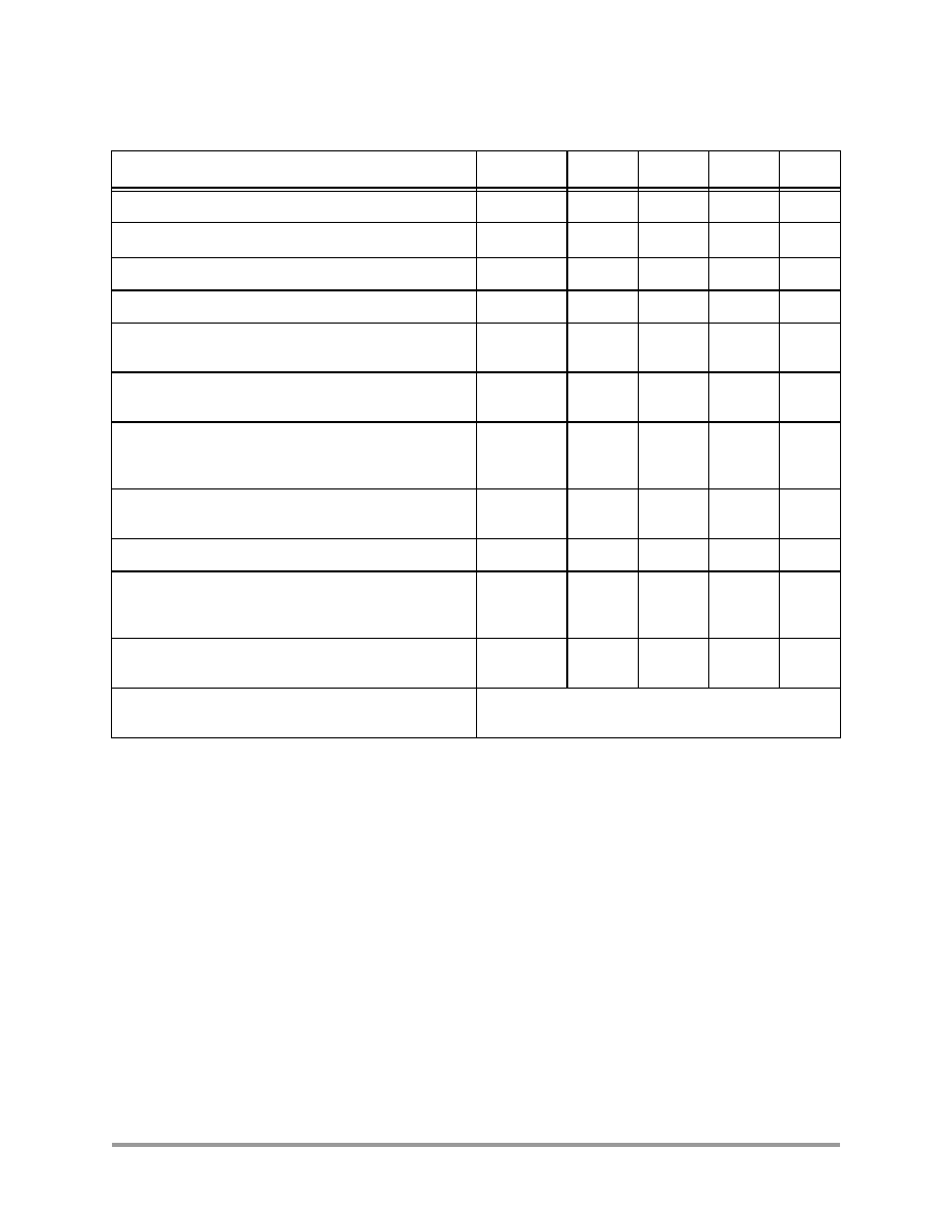
Table 3. Electrical Specifications
(V
D1,2,3
= 3.2 V, V
abc
= 2.6 V, P
in
= 5.0 dBm, Peak measurement at 12.5% duty cycle, 4.6 ms period, T
A
= 25∞C, unless otherwise
noted.)
Characteristic Symbol
Min
Typ
Max
Unit
Frequency Range
BW
880
-
915
MHz
Output Power
P
out
34.5
-
-
dBm
Power Added Efficiency
PAE
50
-
-
%
Minimum Output Power (V
ref
= 0.04, V
abc
= 2.6 V)
-
-
-17
dBm
Power Control Slope (V
ref
= 0.1 to 1.8 V,
V
ref
= 0.01 V)
-
-
50:1
RFVrms
/V
ref
Bleed thru Power (P
in(fo)
-12dBm, V
ref
= 0.04,
V
abc
= 10 k load)
-
-
-36
dBm
RF Leakage Current (I
DD1
+ I
DD2
+I
DD3,
Pin (f
o
)
5.0
dBm)
(V
abc
= 10 k load, V
ref
= 0.04 V)
-
-
35
mA
Output Power Switching Speed (± step input of V
ref
RF
Pout within 1.0 dB of final value)
-
-
1.0
µ
s
Input Return Loss
|S11|
-
-
6.0
dB
Noise Power in Rx band
925 to 935 MHz
935 to 960 MHz
NP
-
-
-
-
-73
-85
dBm
Stability-Spurious Output (Load VSWR 6:1 all phase
angles, Adjust V
D1, 2&3
for specified power)
P
spur
-
-
-30
dBc
Load Mismatch Stress (Load VSWR = 10:1 all phase
angles, 5 seconds, Adjust V
D1, 2&3
for specified power)
No Degradation in Output Power
Before & After Test
F
r
e
e
s
c
a
l
e
S
e
m
i
c
o
n
d
u
c
t
o
r
,
I
Freescale Semiconductor, Inc.
For More Information On This Product,
Go to: www.freescale.com
n
c
.
.
.
4
MRFIC0970 Technical Data
MOTOROLA
Pin Connections
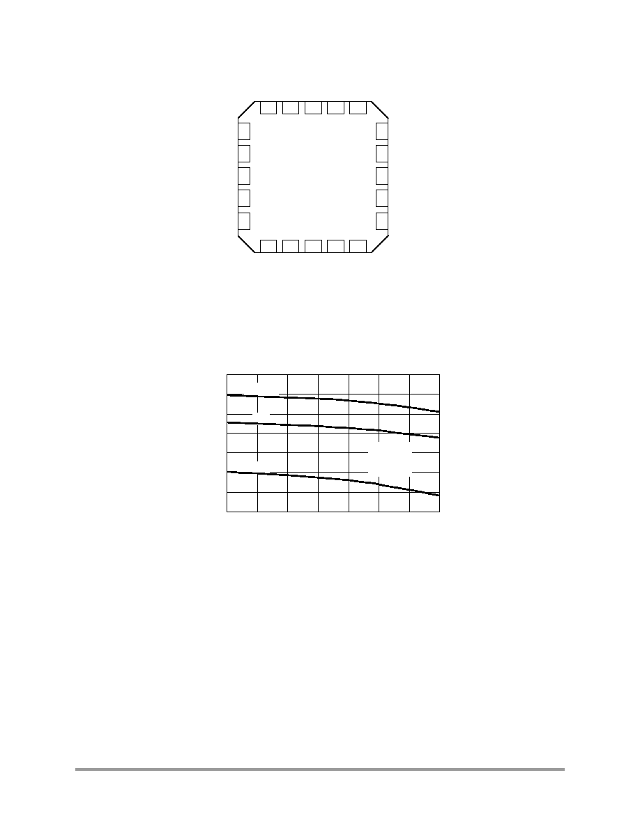
2 Pin Connections
Figure 2. Pin Connections
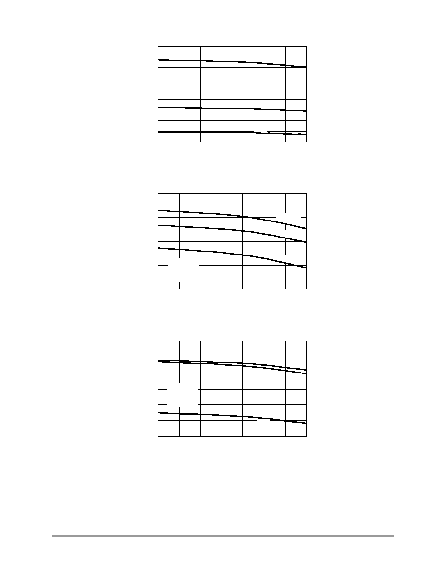
3 Typical Performance Characteristics
Figure 3. Output Power versus Frequency
V
G3
V
G1,2
V
GG1,2
ABC
V
GG3
D2
N.C.
N.C.
N.C.
N.C.
1
2
3
4
5
15
14
13
12
11
6
7
8
9
10
20
19
18
17
16
S1/
GND N.C.
RFin
(G1)
N.C.
D1
N.C.
D3/
RF
OUT
D3/
RF
OUT
D3/
RF
OUT
D3/
RF
OUT
P
o
u
t
,
O
U
T
P
U
T
P
O
W
E
R
(
d
B
m
)
f, FREQUENCY (MHz)
35.6
35.4
35.2
35
34.8
34.6
34.4
34.2
880
885
890
895
900
905
910
915
T
A
= -40∞C
25∞C
85∞C
P
in
= 5.0 dBm
V
DD
= 3.2 V
V
ref
= 1.8 V
F
r
e
e
s
c
a
l
e
S
e
m
i
c
o
n
d
u
c
t
o
r
,
I
Freescale Semiconductor, Inc.
For More Information On This Product,
Go to: www.freescale.com
n
c
.
.
.
Typical Performance Characteristics
MOTOROLA
MRFIC0970 Technical Data
5
Figure 4. Output Power versus Frequency
Figure 5. Power Added Efficiency versus Frequency
Figure 6. Power Added Efficiency versus Frequency
P
o
u
t
,
O
U
T
P
U
T
P
O
W
E
R
(
d
B
m
)
f, FREQUNCY (MHz)
V
DD
= 5.5 V
3.2 V
2.8 V
P
in
= 5.0 dBm
T
A
= 25∞C
V
ref
= 1.8 V
880
885
890
895
900
905
910
915
38
37.5
37
36.5
36
35.5
35
34.5
34
33.5
f, FREQUENCY (MHz)
P
A
E
,
P
O
W
E
R
A
D
D
E
D
E
F
F
I
C
I
E
N
C
Y
(
%
)
65
60
55
50
45
880
885
890
895
900
905
910
915
T
A
= -40∞C
25∞C
85∞C
P
in
= 5.0 dBm
V
DD
= 3.2 V
V
ref
= 1.8 V
f, FREQUENCY (MHz)
P
A
E
,
P
O
W
E
R
A
D
D
E
D
E
F
F
I
C
I
E
N
C
Y
(
%
)
65
60
55
50
45
40
35
880
885
890
895
900
905
910
915
V
DD
= 2.8 V
3.2 V
5.5 V
P
in
= 5.0 dBm
T
A
= 25∞C
V
ref
= 1.8 V
F
r
e
e
s
c
a
l
e
S
e
m
i
c
o
n
d
u
c
t
o
r
,
I
Freescale Semiconductor, Inc.
For More Information On This Product,
Go to: www.freescale.com
n
c
.
.
.
6
MRFIC0970 Technical Data
MOTOROLA
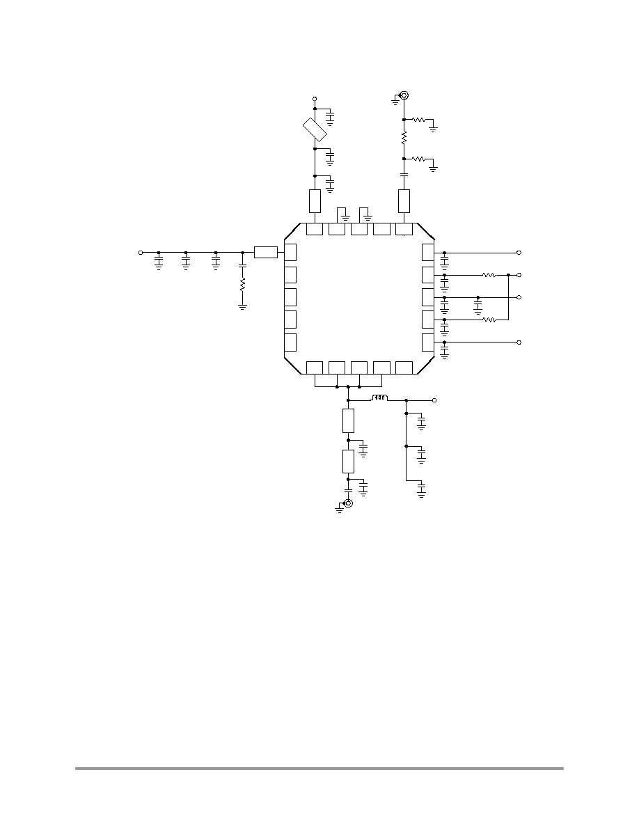
Application Schematic
4 Application Schematic
Figure 7. Application Schematic
N.C.
N.C.
1
2
3
4
5
15
14
13
12
11
6
7
8
9
10
20
19
18
17
16
N.C.
V
DD1
RF In
470
470
680
240
12
1.0 nF
T1
27 pF
6.8 pF
1.0 nF
1.0 nF
1.0 nF
1.0 nF
1.0 nF
0.1 µF
V
G1,2
V
ref
ABC
V
G3
RF Out
1
.
0
n
F
V
DD2
12.55 nH
Coilcraft
1601-10
4700 pF
V
DD3
T2
T3
T4
T5
T1 = .100 in, Z
o
= 50
T2 = .275 in, Z
o
= 50
T3 = .166 in, Z
o
= 50
T4 = .041 in, Z
o
= 50
T5 = .420 in, Z
o
= 50
N.C.
N.C.
N.C.
0
.
0
1
µ
F
4
7
0
0
p
F
3
9
p
F
2
.
7
0.1 µF
1.0 µF
Ferrite Bead
120
100 pF
0.1 µF
0.1 µF
47 µF
F
r
e
e
s
c
a
l
e
S
e
m
i
c
o
n
d
u
c
t
o
r
,
I
Freescale Semiconductor, Inc.
For More Information On This Product,
Go to: www.freescale.com
n
c
.
.
.
Packaging
MOTOROLA
MRFIC0970 Technical Data
7
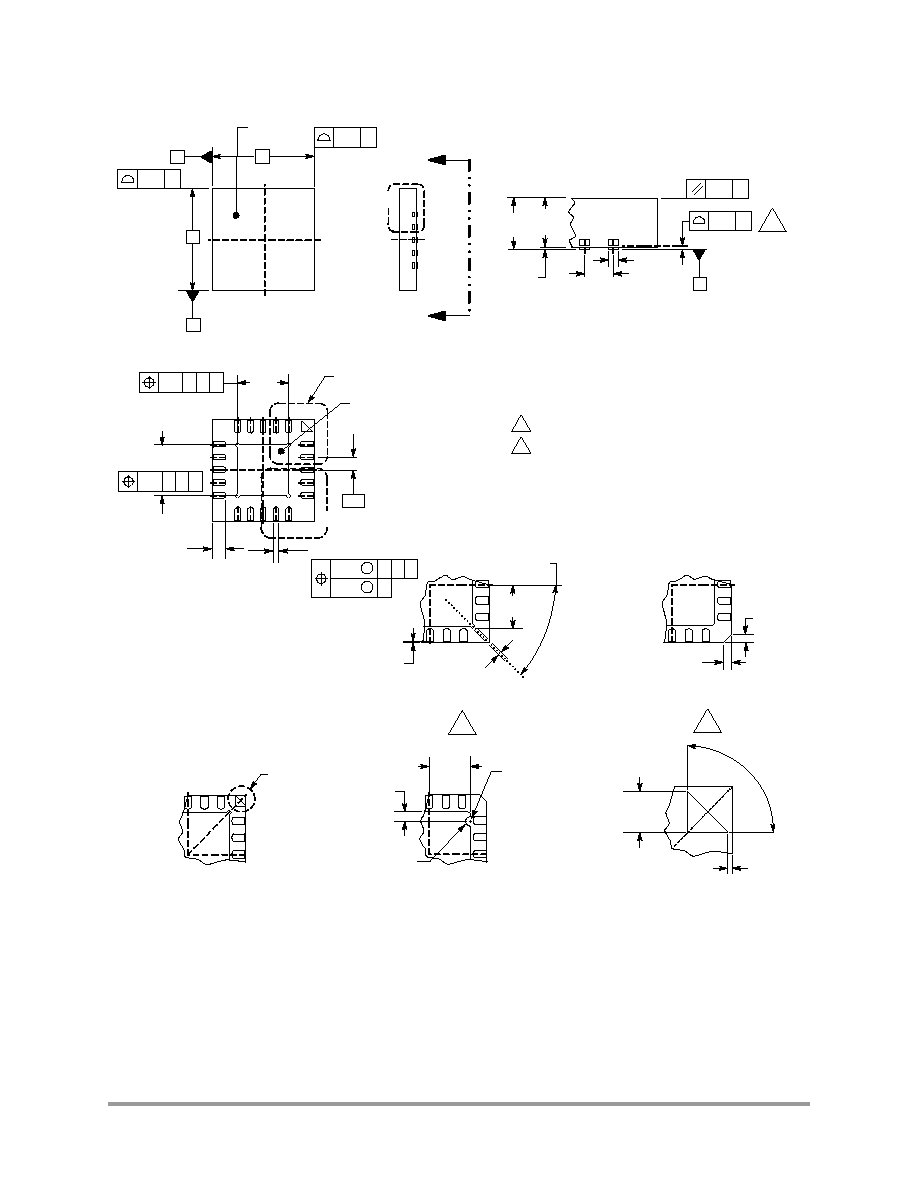
5 Packaging
Figure 8. Outline Dimensions for QFN-20
(Case 1308-02, Issue C)
G
M
M
N
EXPOSED DIE
ATTACH PAD
2.25
16
5
1
20
2.25
20X
0.30
15
11
10
6
0.5
M
0.1
C
M
0.05
C
A B
20X
0.75
0.50
C
0.1
A B
C
0.1
A B
VIEW M-M
DETAIL M
PIN 1 INDEX
1.95
0.18
1.95
16X
PIN 1
INDEX AREA
4
B
C
0.1
2X
2X
C
0.1
A
4
1.0 1.00
0.05
C
0.1
C
0.05
C
SEATING PLANE
5
DETAIL G
VIEW ROTATED 90 CLOCKWISE
(0.5)
(0.24)
0.8 0.75
0.00
(1.19)
(0.27)
0.065
20X
0.015
(45 )
4
PREFERRED CORNER CONFIGURATION
DETAIL N
0.60
0.60
0.24
0.24
4
DETAIL N
CORNER CONFIGURATION OPTION
DETAIL T
DETAIL M
PREFERRED BACKSIDE PIN 1 INDEX
DETAIL T
PREFERRED BACKSIDE PIN 1 INDEX
(90 )
2X
2X 0.39
0.31
0.1
0.0
DETAIL M
BACKSIDE PIN 1 INDEX OPTION
1.1
0.475
0.425
1.0
BACKSIDE
PIN 1 INDEX
0.25
0.15
R
NOTES:
1. DIMENSIONS ARE IN MILLIMETERS.
2. DIMENSIONS AND TOLERANCES PER ASME
Y14.5M, 1994.
3. THE COMPLETE JEDEC DESIGNATOR FOR THIS PACKAGE
IS: HF-PQFP-N.
4. CORNER CHAMFER MAY NOT BE PRESENT. DIMENSIONS
OF OPTIONAL FEATURES ARE FOR REFERENCE ONLY.
5. COPLANARITY APPLIES TO LEADS, CORNER LEADS, AND
DIE ATTACH PAD.
7. FOR ANVIL SINGULATED QFN PACKAGES, MAXIMUM
DRAFT ANGLE IS 12 .
F
r
e
e
s
c
a
l
e
S
e
m
i
c
o
n
d
u
c
t
o
r
,
I
Freescale Semiconductor, Inc.
For More Information On This Product,
Go to: www.freescale.com
n
c
.
.
.
MRFIC0970/D
HOW TO REACH US:
USA/EUROPE/LOCATIONS NOT LISTED:
Motorola Literature Distribution;
P.O. Box 5405, Denver, Colorado 80217
1-303-675-2140 or 1-800-441-2447
JAPAN:
Motorola Japan Ltd.; SPS, Technical Information Center,
3-20-1, Minami-Azabu Minato-ku, Tokyo 106-8573 Japan
81-3-3440-3569
ASIA/PACIFIC:
Motorola Semiconductors H.K. Ltd.; Silicon Harbour
Centre, 2 Dai King Street, Tai Po Industrial Estate,
Tai Po, N.T., Hong Kong
852-26668334
TECHNICAL INFORMATION CENTER:
1-800-521-6274
HOME PAGE:
http://www.motorola.com/semiconductors
Information in this document is provided solely to enable system and software implementers to
use Motorola products. There are no express or implied copyright licenses granted hereunder to
design or fabricate any integrated circuits or integrated circuits based on the information in this
document.
Motorola reserves the right to make changes without further notice to any products herein.
Motorola makes no warranty, representation or guarantee regarding the suitability of its products
for any particular purpose, nor does Motorola assume any liability arising out of the application or
use of any product or circuit, and specifically disclaims any and all liability, including without
limitation consequential or incidental damages. ÏTypicalÓ parameters which may be provided in
Motorola data sheets and/or specifications can and do vary in different applications and actual
performance may vary over time. All operating parameters, including ÏTypicalsÓ must be validated
for each customer application by customerÌs technical experts. Motorola does not convey any
license under its patent rights nor the rights of others. Motorola products are not designed,
intended, or authorized for use as components in systems intended for surgical implant into the
body, or other applications intended to support or sustain life, or for any other application in which
the failure of the Motorola product could create a situation where personal injury or death may
occur. Should Buyer purchase or use Motorola products for any such unintended or unauthorized
application, Buyer shall indemnify and hold Motorola and its officers, employees, subsidiaries,
affiliates, and distributors harmless against all claims, costs, damages, and expenses, and
reasonable attorney fees arising out of, directly or indirectly, any claim of personal injury or death
associated with such unintended or unauthorized use, even if such claim alleges that Motorola
was negligent regarding the design or manufacture of the part.
Motorola and the Stylized M Logo are registered in the U.S. Patent and Trademark Office. All other
product or service names are the property of their respective owners. Motorola, Inc. is an Equal
Opportunity/Affirmative Action Employer.
© Motorola, Inc. 2002
F
r
e
e
s
c
a
l
e
S
e
m
i
c
o
n
d
u
c
t
o
r
,
I
Freescale Semiconductor, Inc.
For More Information On This Product,
Go to: www.freescale.com
n
c
.
.
.