MW5IC2030NBR1 MW5IC2030GNBR1
1
RF Device Data
Freescale Semiconductor
RF LDMOS Wideband Integrated
Power Amplifiers
The MW5IC2030N wideband integrated circuit is designed with on -chip
matching that makes it usable from 1930 to 1990
MHz. This multi -stage
structure is rated for 26 to 28
Volt operation and covers all typical cellular base
station modulation formats.
Final Application
∑ Typical CDMA Performance: V
DD
= 27 Volts, I
DQ1
= 160 mA,
I
DQ2
= 230 mA, P
out
= 5 Watts Avg., Full Frequency Band, IS-95 CDMA
(Pilot, Sync, Paging, Traffic Codes 8 Through 13), Channel Bandwidth =
1.2288 MHz. PAR = 9.8 dB @ 0.01% Probability on CCDF.
Power Gain -- 23 dB
Drain Efficiency -- 20%
ACPR @ 885 kHz Offset -- -49 dBc in 30 kHz Channel Bandwidth
Driver Application
∑ Typical CDMA Performance: V
DD
= 27 Volts, I
DQ1
= 220 mA, I
DQ2
=
240 mA, P
out
= 1 Watt Avg., Full Frequency Band, IS-95 CDMA (Pilot,
Sync, Paging, Traffic Codes 8 Through 13), Channel Bandwidth =
1.2288 MHz. PAR = 9.8 dB @ 0.01% Probability on CCDF.
Power Gain -- 24 dB
ACPR @ 885 kHz Offset -- -63 dBc in 30 kHz Channel Bandwidth
∑ Capable of Handling 10:1 VSWR, @ 27 Vdc, 1990 MHz, 30 Watts CW
Output Power
∑ Stable into a 3:1 VSWR. All Spurs Below -60 dBc @ 0 to 43 dBm CW
P
out
.
∑ On-Chip Matching (50 Ohm Input, >4 Ohm Output)
∑ Integrated Temperature Compensation Capability with Enable/Disable
Function
∑ On-Chip Current Mirror g
m
Reference FET for Self Biasing Application
(1)
∑ Integrated ESD Protection
∑ 200∞C Capable Plastic Package
∑ N Suffix Indicates Lead-Free Terminations. RoHS Compliant.
∑ In Tape and Reel. R1 Suffix = 500 Units per 44 mm, 13 inch Reel
1. Refer to AN1987, Quiescent Current Control for the RF Integrated Circuit Device Family. Go to http://www.freescale.com/rf.
Select Documentation/Application Notes - AN1987.
Document Number: MW5IC2030N
Rev. 7, 1/2006
Freescale Semiconductor
Technical Data
1930 -1990 MHz, 30 W, 26 V
GSM/GSM EDGE, W-CDMA, PHS
RF LDMOS WIDEBAND
INTEGRATED POWER AMPLIFIERS
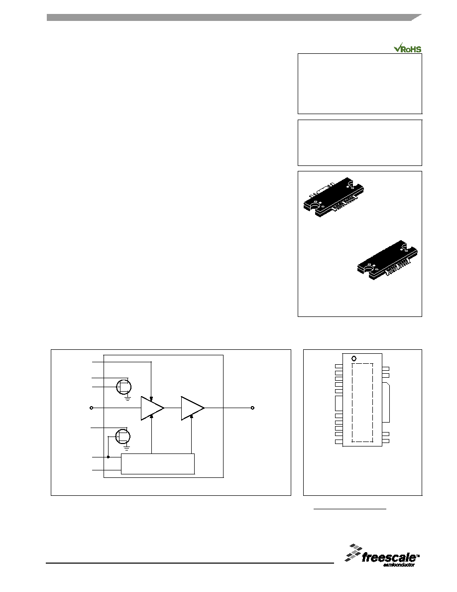
CASE 1329-09
TO-272 WB-16
PLASTIC
MW5IC2030NBR1
MW5IC2030NBR1
MW5IC2030GNBR1
CASE 1329A-03
TO-272 WB-16 GULL
PLASTIC
MW5IC2030GNBR1
Figure 1. Functional Block Diagram
Figure 2. Pin Connections
(Top View)
GND
GND
RF
in
V
RG1
/V
GS1
GND
V
DS1
V
DS2/
RF
out
GND
V
GS2
GND
V
RD2
V
RG2
V
RD1
NC
NC
NC
V
RG1
/V
GS1
RF
in
V
DS1
V
GS2
V
DS2
/RF
out
Quiescent Current
Temperature Compensation
V
RD2
V
RG2
V
RD1
2
3
4
5
6
7
8
16
15
14
13
12
9
10
11
1
Note: Exposed backside flag is source
terminal for transistors.
Freescale Semiconductor, Inc., 2006. All rights reserved.
2
RF Device Data
Freescale Semiconductor
MW5IC2030NBR1 MW5IC2030GNBR1
Table 1. Maximum Ratings
Rating
Symbol
Value
Unit
Drain-Source Voltage
V
DSS
-0.5, +65
Vdc
Gate-Source Voltage
V
GS
-0.5, +15
Vdc
Storage Temperature Range
T
stg
-65 to +175
∞C
Operating Junction Temperature
T
J
200
∞C
Input Power
P
in
20
dBm
Table 2. Thermal Characteristics
Characteristic
Symbol
Value
(1,2)
Unit
Thermal Resistance, Junction to Case
CDMA Application
Stage 1, 27 Vdc, I
DQ
= 160 mA
(P
out
= 5 W CW)
Stage 2, 27 Vdc, I
DQ
= 230 mA
PHS Application
Stage 1, 26 Vdc, I
DQ
= 300 mA
(P
out
= 12.6 W CW)
Stage 2, 26 Vdc, I
DQ
= 1300 mA
R
JC
4.89
1.75
4.85
1.61
∞C/W
Table 3. ESD Protection Characteristics
Test Conditions
Class
Human Body Model
1B (Minimum)
Machine Model
A (Minimum)
Charge Device Model
3 (Minimum)
Table 4. Moisture Sensitivity Level
Test Methodology
Rating
Package Peak Temperature
Unit
Per JESD 22-A113, IPC/JEDEC J-STD-020
3
260
∞C
Table 5. Electrical Characteristics
(T
C
= 25∞C unless otherwise noted)
Characteristic
Symbol
Min
Typ
Max
Unit
CDMA Functional Tests (In Freescale 1900 MHz Test Fixture, 50 hm system) V
DD
= 27 Vdc, I
DQ1
= 160 mA, I
DQ2
= 230 mA, P
out
=
5 W Avg., 1960 MHz, Single-Carrier N-CDMA, 1.2288 MHz Channel Bandwidth Carrier. ACPR measured in 30 kHz Channel Bandwidth
@ ± 885 kHz Offset. PAR = 9.8 dB @ 0.01 Probability on CCDF.
Power Gain
G
ps
21.5
23
--
dB
Drain Efficiency
D
18
20
--
%
Input Return Loss
IRL
--
-18
-10
dB
Adjacent Channel Power Ratio
ACPR
--
-49
-47
dBc
Gain Flatness in 30 MHz BW, 1930-1990 MHz
G
F
--
0.2
0.3
dB
1. MTTF calculator available at http://www.freescale.com/rf. Select Tools/Software/Application Software/Calculators to access
the MTTF calculators by product.
2. Refer to AN1955, Thermal Measurement Methodology of RF Power Amplifiers. Go to http://www.freescale.com/rf.
Select Documentation/Application Notes - AN1955.
(continued)
MW5IC2030NBR1 MW5IC2030GNBR1
3
RF Device Data
Freescale Semiconductor
Table 5. Electrical Characteristics
(T
C
= 25∞C unless otherwise noted)
(continued)
Characteristic
Symbol
Min
Typ
Max
Unit
Typical Performances (In Freescale Test Fixture) V
DD
= 26 Vdc, I
DQ1
= 160 mA, I
DQ2
= 230 mA, P
out
= 5 W, f = 1960 MHz
P
out
@ 1 dB Compression Point, CW
P1dB
--
30
--
W
Deviation from Linear Phase in 30 MHz BW
(Characterized from 1930-1990 MHz)
--
±1
--
∞
Delay
Delay
--
2.25
--
ns
Part-to-Part Phase Variation
--
±10
--
∞
Part-to-Part Gain Variation (Per Lot or Reel)
G
--
±1.5
--
dB
Reference FET to RF FET Scaling Ratio Delta (Stages 1 and 2)
--
10
--
%
Typical PHS Performances (In Freescale Test Fixture, 50 hm system) V
DD
= 26 Vdc, I
DQ1
= 260 mA, I
DQ2
= 1100 mA, P
out
=
12.6 W, 1900 MHz, PHS Signal Mask
Power Gain
G
ps
--
24
--
dB
Drain Efficiency
D
--
25
--
%
Input Return Loss
IRL
--
-15
--
dB
Adjacent Channel Power Ratio
(600 kHz Offset in 192 kHz BW)
ACPR
--
-72
--
dBc
4
RF Device Data
Freescale Semiconductor
MW5IC2030NBR1 MW5IC2030GNBR1
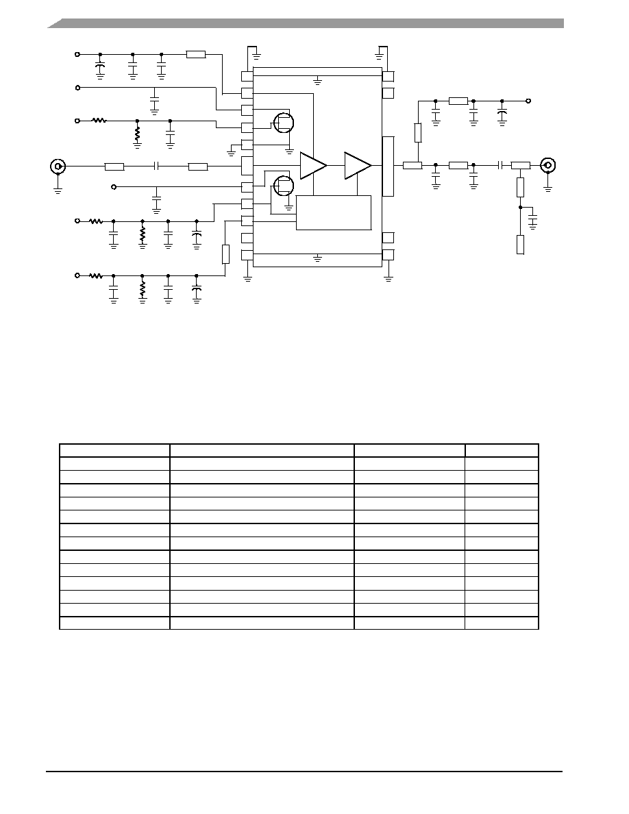
1
16
Figure 3. MW5IC2030NBR1(GNBR1)
Test Circuit Schematic
RF
OUTPUT
RF
INPUT
Z1
V
D2
Z9
Z8
C5
C20
Z3
Z4
Z5
Z6
Z7
C3
C4
C1
V
BIAS2
R2
R5
C10
C16
V
RD2
C13
2
3
4
5
6
7
8
NC
NC
14
15
12
13
+
C8
Z11
V
BIAS1
R1
R4
C11
C15
V
RG1
/V
GS1
C14
V
BIAS R2
11
10
9
NC
Quiescent Current
Temperature
Compensation
C2
NC
C17
+
C18
+
Z2
C7
V
D1
R3
R6
C12
Z10
C9
+
C6
C19
V
RD1
Z7
0.200 x 0.025 Microstrip
Z8
0.274 x 0.050 Microstrip
Z9
0.615 x 0.050 Microstrip
Z10
0.450 x 0.025 Microstrip
Z11
0.340 x 0.014 Microstrip
PCB
Rogers 4350, 0.020,
r
= 3.5
Z1
0.465 x 0.041 Microstrip
Z2
0.518 x 0.041 Microstrip
Z3
0.282 x 0.235 Microstrip
Z4
0.221 x 0.081 Microstrip
Z5
0.489 x 0.041 Microstrip
Z6
0.471 x 0.025 Microstrip
Table 6. MW5IC2030NBR1(GNBR1) Test Circuit Component Designations and Values
Part
Description
Part Number
Manufacturer
C1
1.8 pF High Q Chip Capacitor (0603)
600S1R8AT-250-T
ATC
C2
1.5 pF High Q Chip Capacitor (0603)
600S1R5AT-250-T
ATC
C3
3.9 pF High Q Chip Capacitor (0603)
600S3R9AT-250-T
ATC
C4
6.8 pF High Q Chip Capacitor (0805)
600S6R8AT-250-T
ATC
C5, C6
100 pF Class 1 NPO Chip Capacitors (0805)
GRM215CB1H101CZ01D
Murata
C7
4.7 pF Class 1 NPO Chip Capacitor (0805)
GRM215CB1H4R7CZ01D
Murata
C8, C9, C10, C11
0.1 µF X7R Chip Capacitors (1206)
C1206C104K5RACT
Kemet
C12, C13, C14, C15, C16
0.01 µF Class 2 X7R Chip Capacitors (0805)
C0805C103K5RACT
Kemet
C17, C18
22 µF, 35 V Electrolytic Capacitors
ECE-1AVKS220
Panasonic
C19, C20
330 µF, 50 V Electrolytic Capacitors
ECA-1HM331
Panasonic
R1, R3
1 kW, 5% Chip Resistors (0805)
R2
499 W, 1% Chip Resistor (0805)
R4, R5, R6
100 kW, 5% Chip Resistors (0805)

MW5IC2030NBR1 MW5IC2030GNBR1
5
RF Device Data
Freescale Semiconductor
Figure 4. MW5IC2030NBR1(GNBR1) Test Circuit Component Layout
V
D1
V
D2
R
D2
R
G2
NC
V
G2
R
D1
V
G1
R
G1
Rev 3
MW5IC2030M
CUT
OUT
AREA
C11
C12
R3
R2
R1
R4
C10
R5
C16
C15
C14
C18
C17
C7
C13
R6
C9
C6
C19
C20
C8
C5
C3
C2
C1
C4
Freescale has begun the transition of marking Printed Circuit Boards (PCBs) with the Freescale Semiconductor
signature/logo. PCBs may have either Motorola or Freescale markings during the transition period. These changes will have
no impact on form, fit or function of the current product.