MW5IC970NBR1
1
RF Device Data
Freescale Semiconductor
RF LDMOS Wideband 2-Stage
Power Amplifiers
Designed for broadband commercial and industrial applications with frequen-
cies from 132 MHz to 960 MHz. The high gain and broadband performance of
this device make it ideal for large-signal, common-source amplifier applica-
tions in 28 volt base station equipment. The device has a 2-stage design with
off-chip matching for the input, interstage and output networks to cover the
desired frequency band.
∑ Typical Performance: 800 MHz, 28 Volts, I
DQ1
= 80 mA,
I
DQ2
= 650 mA, P
out
= 70 Watts PEP
Power Gain -- 30 dB
Drain Efficiency -- 48%
∑ Capable of Handling 10:1 VSWR, @ 28 Vdc, 960 MHz, 70 Watts CW
Output Power
Features
∑ Characterized with Series Equivalent Large-Signal Impedance Parameters
∑ Integrated Quiescent Current Temperature Compensation
with Enable/Disable Function
∑ On-Chip Current Mirror g
m
Reference FET for Self Biasing Application
(1)
∑ Integrated ESD Protection
∑ 200∞C Capable Plastic Package
∑ RoHS Compliant
∑ In Tape and Reel. R1 Suffix = 500 Units per 44 mm, 13 inch Reel.
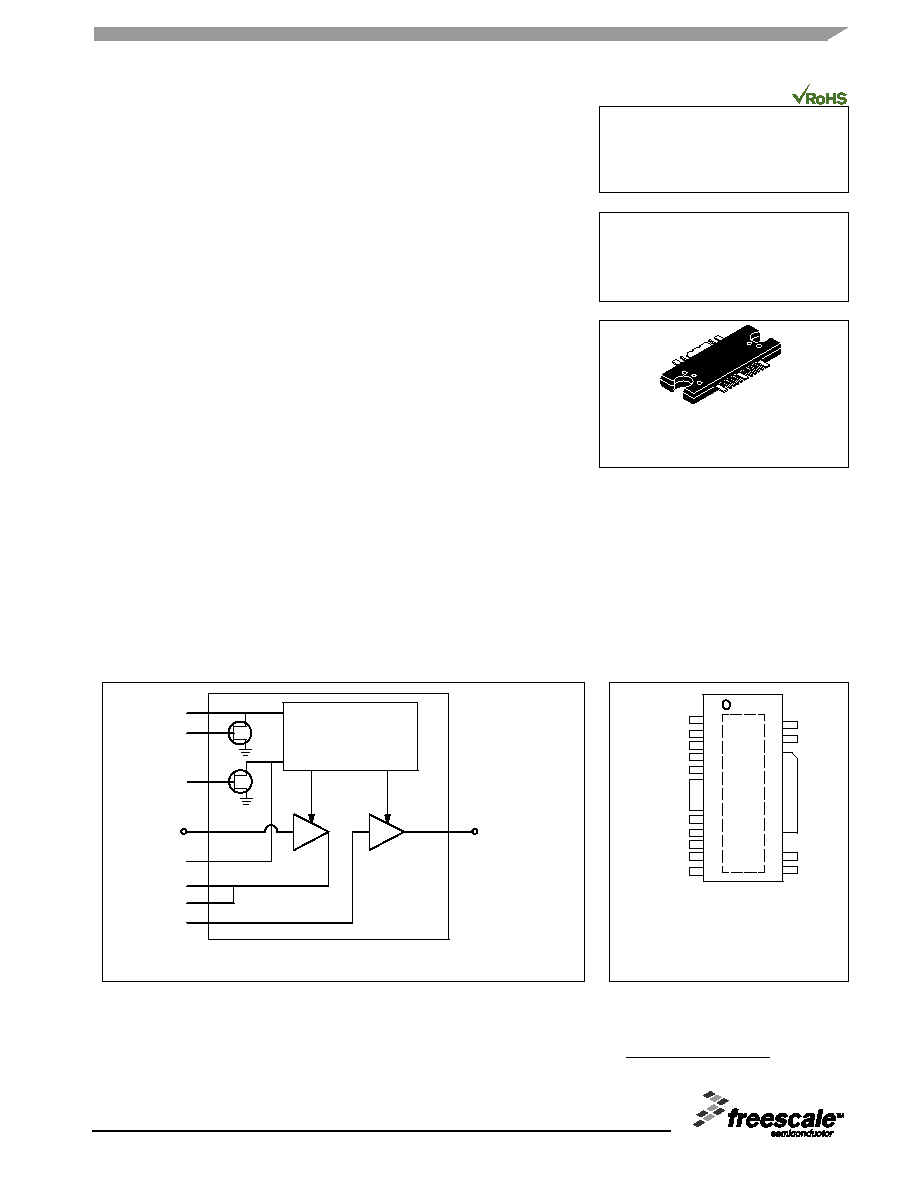
Figure 1. Functional Block Diagram
Figure 2. Pin Connections
V
D1
/RF
out1
RF
in1
V
RD2
V
D2
/RF
out2
Quiescent Current
Temperature Compensation
V
RG2
/V
GS2
V
RG1
/V
GS1
V
RD1
(Top View)
GND
GND
RF
in1
V
D1
/RF
out1
GND
V
RD2
V
D2/
RF
out2
GND
V
D1
/RF
out1
GND
V
RG2
/V
GS2
V
RG1
/V
GS1
V
RD1
NC
RF
in2
NC
2
3
4
5
6
7
8
16
15
14
13
12
9
10
11
1
Note: Exposed backside flag is source
terminal for transistors.
V
D1
/RF
out1
RF
in2
1. Refer to AN1987, Quiescent Current Control for the RF Integrated Circuit Device Family. Go to http://www.freescale.com/rf.
Select Documentation/Application Notes - AN1987.
Document Number: MW5IC970NBR1
Rev. 0, 4/2006
Freescale Semiconductor
Technical Data
800-900 MHz, 70 W, 28 V
RF LDMOS WIDEBAND
2-STAGE POWER AMPLIFIERS
CASE 1329-09
TO-272 WB-16
PLASTIC
MW5IC970NBR1
Freescale Semiconductor, Inc., 2006. All rights reserved.
2
RF Device Data
Freescale Semiconductor
MW5IC970NBR1
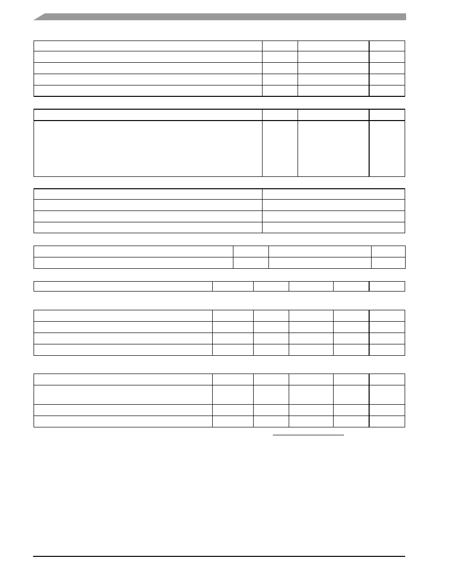
Table 1. Maximum Ratings
Rating
Symbol
Value
Unit
Drain-Source Voltage
V
DSS
- 0.5, + 65
Vdc
Gate-Source Voltage
V
GS
- 0.5, + 15
Vdc
Storage Temperature Range
T
stg
- 65 to +200
∞C
Operating Junction Temperature
T
J
200
∞C
Table 2. Thermal Characteristics
Characteristic
Symbol
Value
(1)
Unit
Thermal Resistance, Junction to Case
Final Application
Stage 1, 28 Vdc, I
DQ
= 80 mA
(P
out
= 70 W CW)
Stage 2, 28 Vdc, I
DQ
= 650 mA
EDGE Application
Stage 1, 28 Vdc, I
DQ
= 80 mA
(P
out
= 35 W CW)
Stage 2, 28 Vdc, I
DQ
= 650 mA
R
JC
5.2
0.8
5.3
0.8
∞C/W
Table 3. ESD Protection Characteristics
Test Methodology
Class
Human Body Model (per JESD22-A114)
1A (Minimum)
Machine Model (per EIA/JESD22-A115)
A (Minimum)
Charge Device Model (per JESD22-C101)
IV (Minimum)
Table 4. Moisture Sensitivity Level
Test Methodology
Rating
Package Peak Temperature
Unit
Per JESD 22-A113, IPC/JEDEC J-STD-020
3
260
∞C
Table 5. Electrical Characteristics
(T
C
= 25∞C unless otherwise noted)
Characteristic
Symbol
Min
Typ
Max
Unit
Functional Tests (In Freescale Test Fixture, 50 ohm system) V
DD
= 28.5 Vdc, I
DQ1
= 80 mA, I
DQ2
= 650 mA, P
out
= 70 W PEP,
f1 = 870.0 MHz, f2 = 870.1 MHz
Power Gain
G
ps
26.5
30
34.5
dB
Drain Efficiency
D
40
48
--
%
Input Return Loss
IRL
--
-12
-10
dB
Intermodulation Distortion
IMD
--
-33
-28
dBc
Typical 800/900 MHz Performances (In Freescale 800/900 MHz Reference Fixture, 50 ohm system) V
DD
= 28 Vdc, I
DQ1
= 80 mA, I
DQ2
=
650 mA, 740-870 MHz, 870-960 MHz
Gain Flatness in 30 MHz Bandwidth @ P
out
= 70 W CW
G
F
--
2
--
dB
Gain Flatness in 30 MHz Instantaneous Bandwidth
@ P
out
= 70 W CW
G
F
--
0.2
--
dB
Delay @ P
out
= 70 W CW Including Output Matching
Delay
--
4.5
--
ns
Part-to-Part Phase Variation @ P
out
= 70 W CW
--
±15
--
∞
1. Refer to AN1955, Thermal Measurement Methodology of RF Power Amplifiers. Go to http://www.freescale.com/rf.
Select Documentation/Application Notes - AN1955.
(continued)
MW5IC970NBR1
3
RF Device Data
Freescale Semiconductor
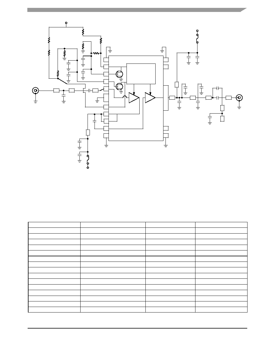
Figure 3. MW5IC970NBR1 Test Circuit Schematic
Z7
0.040 x 0.233 Microstrip
Z8
0.450 x 0.120 Microstrip
Z9
0.100 x 0.066 Microstrip
Z10
1.000 x 0.040 Microstrip
Z11
0.148 x 0.040 Microstrip
PCB
Rogers 4350B, 0.030,
r
= 3.5
Z1
0.485 x 0.066 Microstrip
Z2
0.270 x 0.040 Microstrip
Z3
0.068 x 0.020 Microstrip
Z4
0.950 x 0.040 Microstrip
Z5
0.131 x 0.233 Microstrip
Z6
0.797 x 0.050 Microstrip
1
16
2
3
4
5
6
7
8
NC
14
15
12
13
11
10
9
NC
RF
OUTPUT
C6
C7
C10
C11
Z5
Z6
Z7
Z8
C12
C13
Z10
C14
Z11
Z9
C8
C9
R8
C18
C17
R5
R7
C15
C16
R2
R1
Z3
C2
R3
R4
RF
INPUT
Z1
Z2
C1
R6
V
BIAS
C5
Z4
C3
C4
V
G1R1
V
G2R2
V
D1
F2
V
D2
F1
Quiescent Current
Temperature
Compensation
Table 6. MW5IC970NBR1 Test Circuit Component Designations and Values
Part
Description
Part Number
Manufacturer
C1, C10, C11
3.9 pF Chip Capacitor
600S3R9BT
ATC
C2
56 pF Chip Capacitor
600S560JW
ATC
C3, C8, C14, C15, C17
39 pF Chip Capacitors
GRM40001C0G390J050BD
Murata
C4, C9
10 µF Chip Capacitors
ECJ4YF1H106Z
Panasonic
C5
24 pF Chip Capacitor
600F240JT
ATC
C6, C7
15 pF Chip Capacitors
600F150JT
ATC
C12
4.7 pF Chip Capacitor
600F4R7BT
ATC
C13
0.4 pF Chip Capacitor
600F0R4BT
ATC
C16, C18, C19, C20
0.015 µF Chip Capacitors
GRM400X7R153J050BD
Murata
F1
5A Surface Mount Fuse
1FT5A
Little Fuse
F2
1A Surface Mount Fuse
1FT1A
Little Fuse
R1, R7
681 , Chip Resistors
R2, R5
4.75 k, Chip Resistors
R3, R4, R8
1.21 k, Chip Resistors
R6
267 , Chip Resistor
4
RF Device Data
Freescale Semiconductor
MW5IC970NBR1
C
R6
MW5IC970
Rev. 1
V
G2
V
G1
R8
R7
R4
R3
R1
R5
R2
C18
C17
C16
C15
C2
C5
C1
C3
C4
V
D1
F2
V
D2
F1
C9
C8
C7
C6
C11
C10
C12
C13
C14
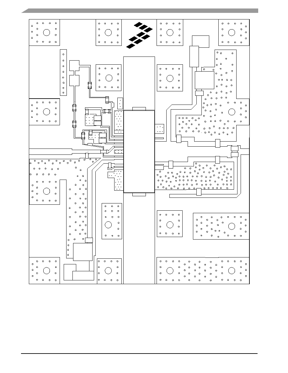
Figure 4. MW5IC970NBR1 Test Circuit Component Layout

MW5IC970NBR1
5
RF Device Data
Freescale Semiconductor
TYPICAL CHARACTERISTICS
960
-40
60
800
-40
60
IRL
G
ps
IMD
f, FREQUENCY (MHz)
V
DD
= 28.5 Vdc, P
out
= 35 W (Avg.)
I
DQ1
= 80 mA, I
DQ2
= 650 mA
100 kHz Tone Spacing
40
40
20
20
0
0
-20
-20
840
880
920
Figure 5. Two-Tone Wideband Performance
@ P
out
= 35 Watts (Avg.)
PAE
PA
E
, POWER ADDED EFFICIENCY (%)
G
ps
, POWER GAIN (dB)
IRL, INPUT RETURN LOSS (dB)
IMD, INTERMODULA
TION DIST
OR
TION (dBc)
P
out
, OUTPUT POWER (WATTS) PEP
100
27
32
1
I
DQ2
= 975 mA
V
DD
= 28.5 Vdc, I
DQ1
= 80 mA
f1 = 870 MHz, f2 = 870.1 MHz
Two-Tone Measurements
100 kHz Tone Spacing
31
30
28
10
200
Figure 6. Two-Tone Power Gain versus
Output Power
G
ps
, POWER GAIN (dB)
300
-70
-10
1
7th Order
V
DD
= 28.5 Vdc
I
DQ1
= 80 mA, I
DQ2
= 650 mA
f1 = 870 MHz, f2 = 870.1 MHz
Two-Tone Measurements
100 kHz Tone Spacing
5th Order
3rd Order
10
-20
-30
-40
-50
-60
P
out
, OUTPUT POWER (WATTS) PEP
Figure 7. Intermodulation Distortion Products
versus Output Power
IMD,
INTERMODULA
TION DIST
OR
TION (dBc)
10
-55
-20
0.1
7th Order
TWO-TONE SPACING (MHz)
5th Order
3rd Order
-25
-30
-35
-40
-45
-50
1
200
Figure 8. Intermodulation Distortion Products
versus Tone Spacing
IMD,
INTERMODULA
TION DIST
OR
TION (dBc)
1000
20
34
0.1
0
70
V
DD
= 28.5 Vdc, I
DQ1
= 80 mA
I
DQ2
= 650 mA, f = 870 MHz
T
C
= 25
_C
85
_C
-30
_C
25
_C
85
_C
10
1
32
30
28
26
24
22
60
50
40
30
20
10
P
out
, OUTPUT POWER (WATTS) CW
Figure 9. Power Gain and Power Added
Efficiency versus CW Output Power
G
ps
, POWER GAIN (dB)
PA
E
,
POWER ADDED EFFICIENCY
(
%
)
G
ps
820
860
900
940
29
100
100
812 mA
650 mA
488 mA
325 mA
V
DD
= 28.5 Vdc, P
out
= 35 W (PEP)
I
DQ1
= 80 mA, I
DQ2
= 650 mA
Two-Tone Measurements
(f1 + f2)/2 = Center Frequency of 870 MHz
100
PAE
-30
_C
6
RF Device Data
Freescale Semiconductor
MW5IC970NBR1
TYPICAL CHARACTERISTICS
P
out
, OUTPUT POWER (WATTS) CW
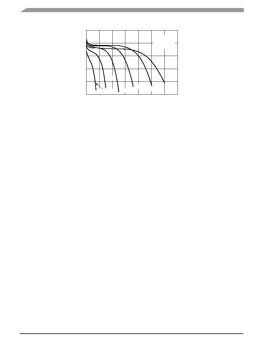
Figure 10. Power Gain versus Output Power
16 V
I
DQ1
= 80 mA
I
DQ2
= 650 mA
f = 870 MHz
V
DD
= 12 V
100
27
32
0
80
31
30
29
28
20
40
60
G
ps
, POWER GAIN (dB)
120
140
20 V
24 V
28.5 V
32 V
MW5IC970NBR1
7
RF Device Data
Freescale Semiconductor
PACKAGE DIMENSIONS
TO-272 WB-16
PLASTIC
.224 BSC
CASE 1329-09
ISSUE L
NOTES:
1. CONTROLLING DIMENSION: INCH.
2. INTERPRET DIMENSIONS AND TOLERANCES PER
ASME Y14.5M-1994.
3. DATUM PLANE -H- IS LOCATED AT TOP OF LEAD
AND IS COINCIDENT WITH THE LEAD WHERE THE
LEAD EXITS THE PLASTIC BODY AT THE TOP OF
THE PARTING LINE.
4. DIMENSIONS "D" AND "E1" DO NOT INCLUDE
MOLD PROTRUSION. ALLOWABLE PROTRUSION
IS .006 (0.15) PER SIDE. DIMENSIONS "D" AND "E1"
DO INCLUDE MOLD MISMATCH AND ARE
DETERMINED AT DATUM PLANE -H-.
5. DIMENSIONS "b", "b1", "b2" AND "b3" DO NOT
INCLUDE DAMBAR PROTRUSION. ALLOWABLE
DAMBAR PROTRUSION SHALL BE .005 (0.13)
TOTAL IN EXCESS OF THE "b", "b1", "b2" AND "b3"
DIMENSIONS AT MAXIMUM MATERIAL CONDITION.
6. HATCHING REPRESENTS THE EXPOSED AREA OF
THE HEAT SLUG.
7. DIM A2 APPLIES WITHIN ZONE "J" ONLY.
C
H
A
SEATING
PLANE
DATUM
PLANE
Y
Y
DIM
A
MIN
MAX
MIN
MAX
MILLIMETERS
.100
.104
2.54
2.64
INCHES
M
.600
---
15.24
---
N
.270
---
6.86
---
D
.928
.932
23.57
23.67
D1
E
.551
.559
14.00
14.20
E1
.353
.357
8.97
9.07
b
.011
.017
0.28
0.43
b1
.037
.043
0.94
1.09
b2
.037
.043
0.94
1.09
c1
.007
.011
.18
.28
e
r1
.063
.068
1.6
1.73
aaa
.054 BSC
.004
1.37 BSC
.10
e1
.040 BSC
1.02 BSC
e2
5.69 BSC
b3
.225
.231
5.72
5.87
c1
B
b3
A
E1
r1
e
D
4X
b1
D1
E
10X
b
PIN ONE
INDEX
6X
e1
4X
e2
b2
M
aaa
C A
M
aaa
C A
M
aaa
C A
M
aaa
C A
M
aaa
C A
««««««
««««««
««««««
««««««
««««««
««««««
««««««
««««««
««««««
««««««
««««««
««««««
M
N
VIEW Y-Y
.150 BSC
e3
3.81 BSC
2X
e3
A1
A1
.038
.044
0.96
1.12
.810 BSC
20.57 BSC
NOTE 6
2X
B
ZONE "J"
A2
7
F
.025 BSC
0.64 BSC
F
E1
E2
.346
.350
8.79
8.89
A2
.040
.042
1.02
1.07
E2

8
RF Device Data
Freescale Semiconductor
MW5IC970NBR1
Information in this document is provided solely to enable system and software
implementers to use Freescale Semiconductor products. There are no express or
implied copyright licenses granted hereunder to design or fabricate any integrated
circuits or integrated circuits based on the information in this document.
Freescale Semiconductor reserves the right to make changes without further notice to
any products herein. Freescale Semiconductor makes no warranty, representation or
guarantee regarding the suitability of its products for any particular purpose, nor does
Freescale Semiconductor assume any liability arising out of the application or use of
any product or circuit, and specifically disclaims any and all liability, including without
limitation consequential or incidental damages. "Typical" parameters that may be
provided in Freescale Semiconductor data sheets and/or specifications can and do
vary in different applications and actual performance may vary over time. All operating
parameters, including "Typicals", must be validated for each customer application by
customer's technical experts. Freescale Semiconductor does not convey any license
under its patent rights nor the rights of others. Freescale Semiconductor products are
not designed, intended, or authorized for use as components in systems intended for
surgical implant into the body, or other applications intended to support or sustain life,
or for any other application in which the failure of the Freescale Semiconductor product
could create a situation where personal injury or death may occur. Should Buyer
purchase or use Freescale Semiconductor products for any such unintended or
unauthorized application, Buyer shall indemnify and hold Freescale Semiconductor
and its officers, employees, subsidiaries, affiliates, and distributors harmless against all
claims, costs, damages, and expenses, and reasonable attorney fees arising out of,
directly or indirectly, any claim of personal injury or death associated with such
unintended or unauthorized use, even if such claim alleges that Freescale
Semiconductor was negligent regarding the design or manufacture of the part.
Freescalet and the Freescale logo are trademarks of Freescale Semiconductor, Inc.
All other product or service names are the property of their respective owners.
Freescale Semiconductor, Inc. 2006. All rights reserved.
How to Reach Us:
Home Page:
www.freescale.com
E-mail:
support@freescale.com
USA/Europe or Locations Not Listed:
Freescale Semiconductor
Technical Information Center, CH370
1300 N. Alma School Road
Chandler, Arizona 85224
+1-800-521-6274 or +1-480-768-2130
support@freescale.com
Europe, Middle East, and Africa:
Freescale Halbleiter Deutschland GmbH
Technical Information Center
Schatzbogen 7
81829 Muenchen, Germany
+44 1296 380 456 (English)
+46 8 52200080 (English)
+49 89 92103 559 (German)
+33 1 69 35 48 48 (French)
support@freescale.com
Japan:
Freescale Semiconductor Japan Ltd.
Headquarters
ARCO Tower 15F
1-8-1, Shimo-Meguro, Meguro-ku,
Tokyo 153-0064
Japan
0120 191014 or +81 3 5437 9125
support.japan@freescale.com
Asia/Pacific:
Freescale Semiconductor Hong Kong Ltd.
Technical Information Center
2 Dai King Street
Tai Po Industrial Estate
Tai Po, N.T., Hong Kong
+800 2666 8080
support.asia@freescale.com
For Literature Requests Only:
Freescale Semiconductor Literature Distribution Center
P.O. Box 5405
Denver, Colorado 80217
1-800-441-2447 or 303-675-2140
Fax: 303-675-2150
LDCForFreescaleSemiconductor@hibbertgroup.com
Document Number: MW5IC970NBR1
Rev. 0, 4/2006