MW6IC2240NBR1 MW6IC2240GNBR1
1
RF Device Data
Freescale Semiconductor
RF LDMOS Wideband Integrated
Power Amplifiers
The MW6IC2240N wideband integrated circuit is designed with on-chip
matching that makes it usable from 2110 to 2170 MHz. This multi -stage
structure is rated for 26 to 32 Volt operation and covers all typical cellular base
station modulation formats.
Final Application
∑ Typical 2-Carrier W-CDMA Performance: V
DD
= 28 Volts, I
DQ1
=
210 mA, I
DQ2
= 370 mA, P
out
= 4.5 Watts Avg., Full Frequency Band
(2110-2170 MHz), Channel Bandwidth = 3.84 MHz, PAR = 8.5 dB
@ 0.01% Probability on CCDF.
Power Gain -- 28 dB
Power Added Efficiency -- 15%
IM3 @ 10 MHz Offset -- -43 dBc in 3.84 MHz Bandwidth
ACPR @ 5 MHz Offset -- -46 dBc in 3.84 MHz Bandwidth
Driver Application
∑ Typical 2-Carrier W-CDMA Performance: V
DD
= 28 Volts, I
DQ1
=
300 mA, I
DQ2
= 320 mA, P
out
= 25 dBm, Full Frequency Band (2110-
2170 MHz), Channel Bandwidth = 3.84 MHz, PAR = 8.5 dB @ 0.01%
Probability on CCDF.
Power Gain -- 29 dB
IM3 @ 10 MHz Offset -- -59 dBc in 3.84 MHz Bandwidth
ACPR @ 5 MHz Offset -- -62 dBc in 3.84 MHz Bandwidth
∑ Capable of Handling 3:1 VSWR, @ 28 Vdc, 2170 MHz, 20 Watts CW
Output Power
∑ Stable into a 3:1 VSWR. All Spurs Below -60 dBc @ 100 mW to 10 W CW
P
out
.
∑ Characterized with Series Equivalent Large-Signal Impedance Parameters
and Common Source Scattering Parameters
∑ On-Chip Matching (50 Ohm Input, DC Blocked, >3 Ohm Output)
∑ Integrated Quiescent Current Temperature Compensation
with Enable/Disable Function
∑ Integrated ESD Protection
∑ 200∞C Capable Plastic Package
∑ N Suffix Indicates Lead-Free Terminations. RoHS Compliant.
∑ In Tape and Reel. R1 Suffix = 500 Units per 44 mm, 13 inch Reel
Document Number: MW6IC2240N
Rev. 1, 1/2006
Freescale Semiconductor
Technical Data
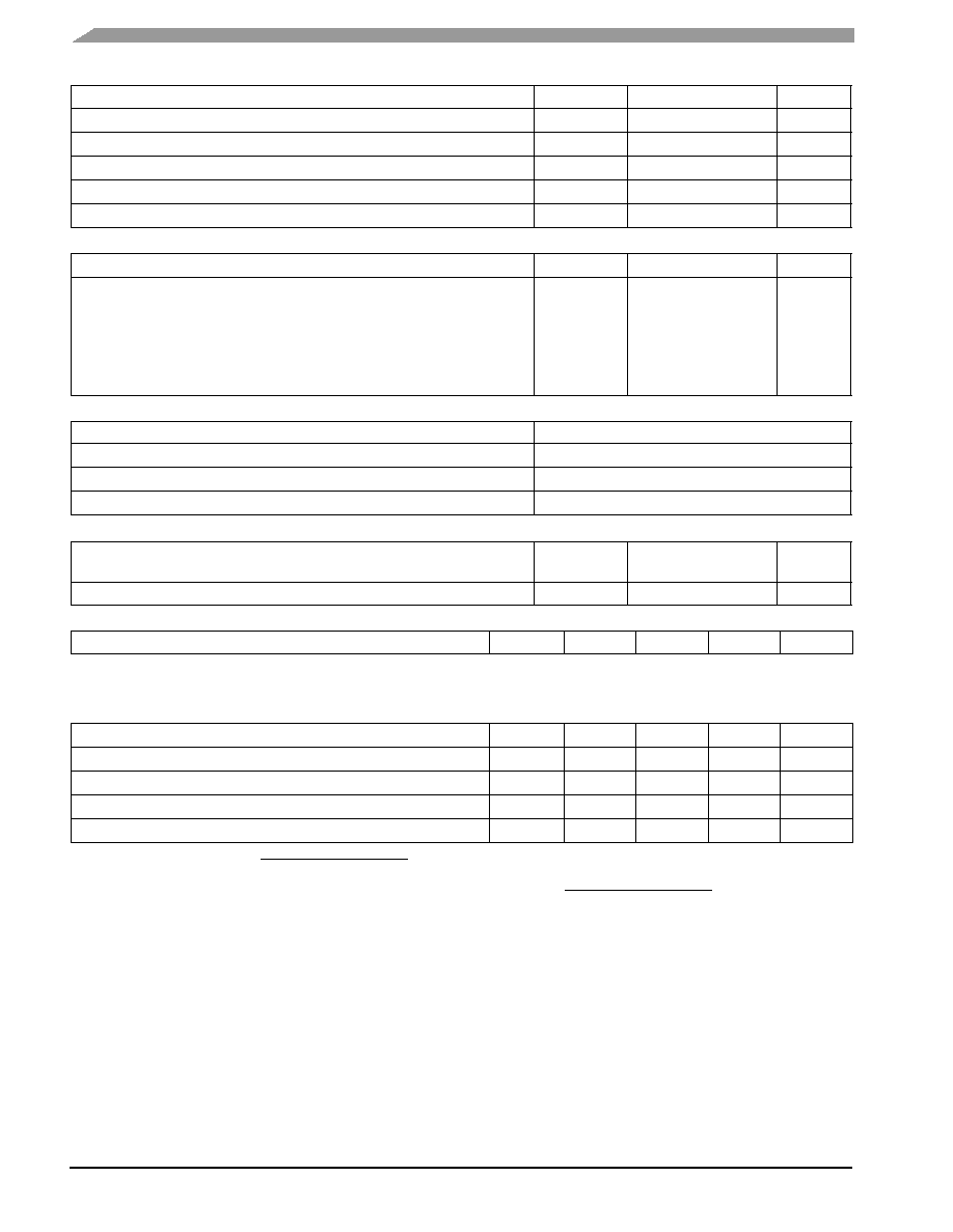
2110-2170 MHz, 4.5 W AVG., 28 V
2 x W-CDMA
RF LDMOS WIDEBAND
INTEGRATED POWER AMPLIFIERS
MW6IC2240NBR1
MW6IC2240GNBR1
CASE 1329-09
TO-272 WB-16
PLASTIC
MW6IC2240NBR1
CASE 1329A-03
TO-272 WB-16 GULL
PLASTIC
MW6IC2240GNBR1
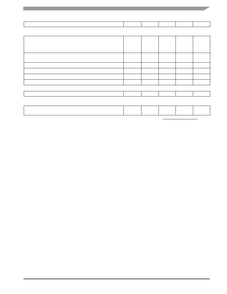
Figure 1. Functional Block Diagram
Figure 2. Pin Connections
(Top View)
GND
NC
RF
in
V
GS1
GND
RF
out
/
V
DS2
GND
1
2
3
4
5
6
7
8
16
15
14
13
12
V
GS2
9
10
GND
11
Quiescent Current
Temperature Compensation
V
DS1
RF
in
V
GS1
RF
out
/V
DS2
V
GS2
V
DS1
NC
NC
NC
V
DS1
NC
NC
Note: Exposed backside flag is source
terminal for transistors.
V
DS1
Freescale Semiconductor, Inc., 2006. All rights reserved.
2
RF Device Data
Freescale Semiconductor
MW6IC2240NBR1 MW6IC2240GNBR1
Table 1. Maximum Ratings
Rating
Symbol
Value
Unit
Drain-Source Voltage
V
DSS
-0.5, +68
Vdc
Gate-Source Voltage
V
GS
-0.5, +6
Vdc
Storage Temperature Range
T
stg
-65 to +200
∞C
Operating Junction Temperature
T
J
200
∞C
Input Power
P
in
23
dBm
Table 2. Thermal Characteristics
Characteristic
Symbol
Value
(1,2)
Unit
Thermal Resistance, Junction to Case
W-CDMA Application
Stage 1, 28 Vdc, I
DQ
= 210 mA
(P
out
= 4.5 W Avg.)
Stage 2, 28 Vdc, I
DQ
= 370 mA
W-CDMA Application
Stage 1, 28 Vdc, I
DQ
= 110 mA
(P
out
= 40 W CW)
Stage 2, 28 Vdc, I
DQ
= 370 mA
R
JC
1.8
1.0
2.0
0.87
∞C/W
Table 3. ESD Protection Characteristics
Test Methodology
Class
Human Body Model (per JESD22-A114)
1A (Minimum)
Machine Model (per EIA/JESD22-A115)
A (Minimum)
Charge Device Model (per JESD22-C101)
III (Minimum)
Table 4. Moisture Sensitivity Level
Test Methodology
Rating
Package Peak
Temperature
Unit
Per JESD 22-A113, IPC/JEDEC J-STD-020
3
260
∞C
Table 5. Electrical Characteristics
(T
C
= 25∞C unless otherwise noted)
Characteristic
Symbol
Min
Typ
Max
Unit
Functional Tests (In Freescale Wideband 2110-2170 MHz Test Fixture, 50 ohm system) V
DD
= 28 Vdc, I
DQ1
= 210 mA, I
DQ2
= 370 mA, P
out
= 4.5 W Avg., f1 = 2112.5 MHz, f2 = 2122.5 MHz and f1 = 2157.5 MHz, f2 = 2167.5 MHz, 2-Carrier W-CDMA, 3.84 MHz Channel
Bandwidth Carriers. ACPR measured in 3.84 MHz Channel Bandwidth @ ±5 MHz Offset. IM3 measured in 3.84 MHz Channel Bandwidth @
±10 MHz Offset. PAR = 8.5 dB @ 0.01% Probability on CCDF.
Power Gain
G
ps
25.5
28
30
dB
Power Added Efficiency
PAE
13.7
15
--
%
Intermodulation Distortion
IM3
--
-43
-40
dBc
Adjacent Channel Power Ratio
ACPR
--
-46
-43
dBc
Input Return Loss
IRL
--
-15
-10
dB
1. MTTF calculator available at http://www.freescale.com/rf. Select Tools/Software/Application Software/Calculators to access
the MTTF calculators by product.
2. Refer to AN1955, Thermal Measurement Methodology of RF Power Amplifiers. Go to http://www.freescale.com/rf.
Select Documentation/Application Notes - AN1955.
(continued)
MW6IC2240NBR1 MW6IC2240GNBR1
3
RF Device Data
Freescale Semiconductor
Table 5. Electrical Characteristics
(T
C
= 25∞C unless otherwise noted)
(continued)
Characteristic
Symbol
Min
Typ
Max
Unit
Typical Performances (In Freescale Test Fixture, 50 hm system) V
DD
= 28 Vdc, I
DQ1
= 210 mA, I
DQ2
= 370 mA,
2110 MHz<Frequency<2170 MHz
Video Bandwidth
(Tone Spacing from 100 kHz to VBW)
IMD3 = IMD3 @ VBW frequency - IMD3 @ 100 kHz <1 dBc (both
sidebands)
VBW
--
30
--
MHz
Quiescent Current Accuracy over Temperature
with 18 k Gate Feed Resistors (-10 to 85∞C)
(1)
I
QT
--
±5
--
%
Gain Flatness in 30 MHz Bandwidth @ P
out
= 1 W CW
G
F
--
0.2
--
dB
Deviation from Linear Phase in 30 MHz Bandwidth @ P
out
= 1 W CW
--
±1
--
∞
Delay @ P
out
= 1 W CW Including Output Matching
Delay
--
2.8
--
ns
Part-to-Part Phase Variation @ P
out
= 1 W CW
--
±9
--
∞
Table 6. Electrical Characteristics
(T
C
= 25∞C unless otherwise noted)
Characteristic
Symbol
Min
Typ
Max
Unit
Typical Performances (In Freescale Test Fixture, 50 hm system) V
DD
= 28 Vdc, I
DQ1
= 110 mA, I
DQ2
= 370 mA,
2110 MHz<Frequency<2170 MHz
Saturated Pulsed Output Power
(8 µsec(on), 1 msec(off))
P
sat
--
60
--
W
1. Refer to AN1977, Quiescent Current Thermal Tracking Circuit in the RF Integrated Circuit Family. Go to http://www.freescale.com/rf. Select
Documentation/Application Notes - AN1977.
4
RF Device Data
Freescale Semiconductor
MW6IC2240NBR1 MW6IC2240GNBR1
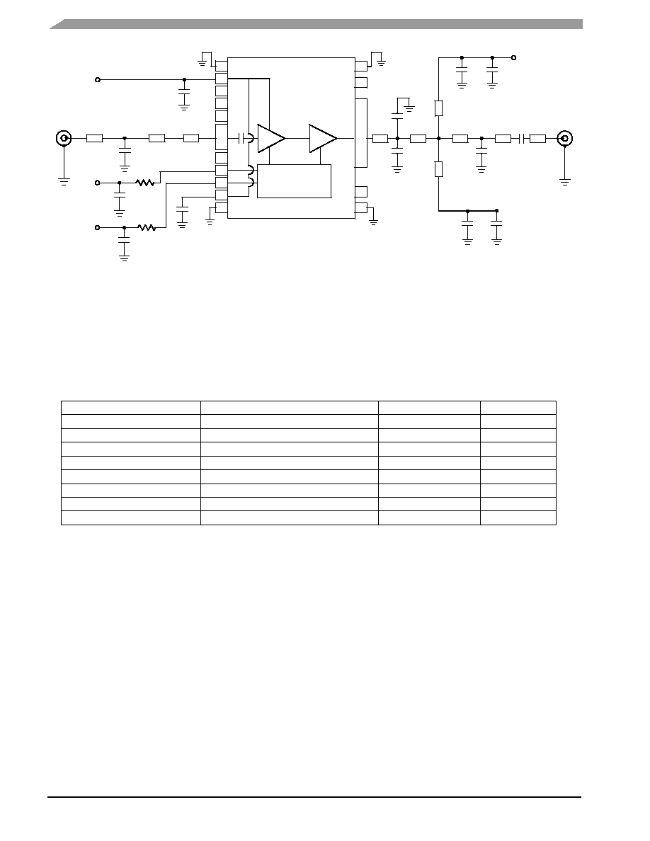
Z7*
0.94 x 0.090 Microstrip
Z8
0.34 x 0.090 Microstrip
Z9, Z10
1.00 x 0.080 Microstrip
PCB
Taconic TLX8-0300, 0.030,
r
= 2.55
* Variable for tuning
Z1*
1.73 x 0.090 Microstrip
Z2*
0.47 x 0.090 Microstrip
Z3
0.13 x 0.040 Microstrip
Z4*
0.22 x 0.315 Microstrip
Z5*
0.34 x 0.315 Microstrip
Z6*
0.34 x 0.090 Microstrip
Figure 3. MW6IC2240NBR1(GNBR1)
Test Circuit Schematic
R1
R2
Z2
RF
INPUT
V
G1
V
G2
Z4
Z5
RF
OUTPUT
C8
C4
C6
V
D2
1
2
3
4
5
6
7
8
14
13
12
11
10
9
15
16
NC
NC
NC
NC
NC
DUT
Z3
C10
C13
V
D1
Z9
Quiescent Current
Temperature
Compensation
Z1
NC
Z10
Z6
Z7
Z8
C1
C2
C5
C7
C3
C12
C11
C9
Table 7. MW6IC2240NBR1(GNBR1) Test Circuit Component Designations and Values
Part
Description
Part Number
Manufacturer
C1, C2
1.5 pF 100B Chip Capacitors
100B1R5BW
ATC
C3
1.8 pF 100B Chip Capacitor
100B1R8BW
ATC
C4, C5
6.8 pF 100B Chip Capacitors
100B6R8CW
ATC
C6, C7, C10, C11, C12, C13
4.7 µF Chip Capacitors (1812)
C4532X5R1H475MT
TDK
C8
8.2 pF 100B Chip Capacitor
100B8R2CW
ATC
C9
0.5 pF 100B Chip Capacitor
100B0R5BW
ATC
R1
18 kW, 1/4 W Chip Resistor (1206)
R2
8.2 kW, 1/4 W Chip Resistor (1206)
MW6IC2240NBR1 MW6IC2240GNBR1
5
RF Device Data
Freescale Semiconductor
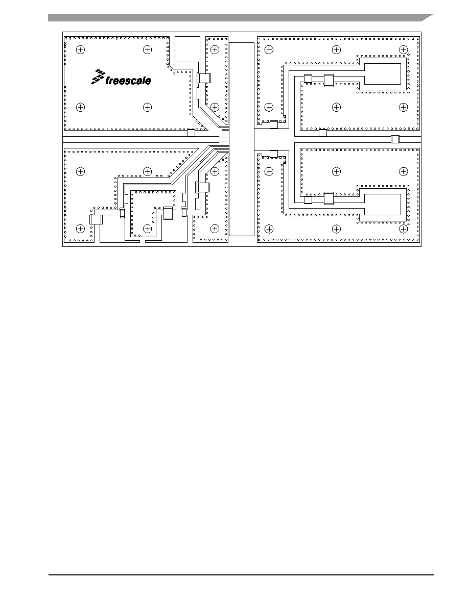
Figure 4. MW6IC2240NBR1(GNBR1) Test Circuit Component Layout
MW6IC2240, Rev. 1
V
D1
C13
C9
C10
C12
R2
R1
V
G1
V
G2
C11
C5
C7
C8
C3
C2
C1
C4
C6
V
D2
CUT
OUT
AREA