MW6S004NT1
1
RF Device Data
Freescale Semiconductor
RF Power Field Effect Transistor
N-Channel Enhancement-Mode Lateral MOSFET
Designed for Class A or Class AB base station applications with frequencies
up to 2000 MHz. Suitable for analog and digital modulation and multicarrier
amplifier applications.
∑ Typical Two-Tone Performance @ 1960 MHz, 28 Volts, I
DQ
= 50 mA,
P
out
= 4 Watts PEP
Power Gain -- 18 dB
Drain Efficiency -- 33%
IMD -- -34 dBc
∑ Typical Two-Tone Performance @ 900 MHz, 28 Volts, I
DQ
= 50 mA,
P
out
= 4 Watts PEP
Power Gain -- 19 dB
Drain Efficiency -- 33%
IMD -- -39 dBc
∑ Capable of Handling 5:1 VSWR, @ 28 Vdc, 1960 MHz, 4 Watts CW Output
Power
Features
∑ Characterized with Series Equivalent Large-Signal Impedance Parameters
∑ On-Chip RF Feedback for Broadband Stability
∑ Integrated ESD Protection
∑ RoHS Compliant
∑ In Tape and Reel. T1 Suffix = 1000 Units per 12 mm, 7 inch Reel.
Table 1. Maximum Ratings
Rating
Symbol
Value
Unit
Drain-Source Voltage
V
DSS
-0.5, +68
Vdc
Gate-Source Voltage
V
GS
-0.5, +12
Vdc
Storage Temperature Range
T
stg
- 65 to +150
∞C
Operating Junction Temperature
T
J
150
∞C
Table 2. Thermal Characteristics
Characteristic
Symbol
Value (1,2)
Unit
Thermal Resistance, Junction to Case
Case Temperature 76∞C, 4 W PEP, Two-Tone
Case Temperature 79∞C, 4 W CW
R
JC
8.8
8.5
∞C/W
Table 3. ESD Protection Characteristics
Test Methodology
Class
Human Body Model (per JESD22-A114)
1A (Minimum)
Machine Model (per EIA/JESD22-A115)
A (Minimum)
Charge Device Model (per JESD22-C101)
III (Minimum)
1. MTTF calculator available at http://www.freescale.com/rf. Select Tools/Software/Application Software/Calculators to access
the MTTF calculators by product.
2. Refer to AN1955, Thermal Measurement Methodology of RF Power Amplifiers. Go to http://www.freescale.com/rf.
Select Documentation/Application Notes - AN1955.
Document Number: MW6S004N
Rev. 1, 4/2006
Freescale Semiconductor
Technical Data
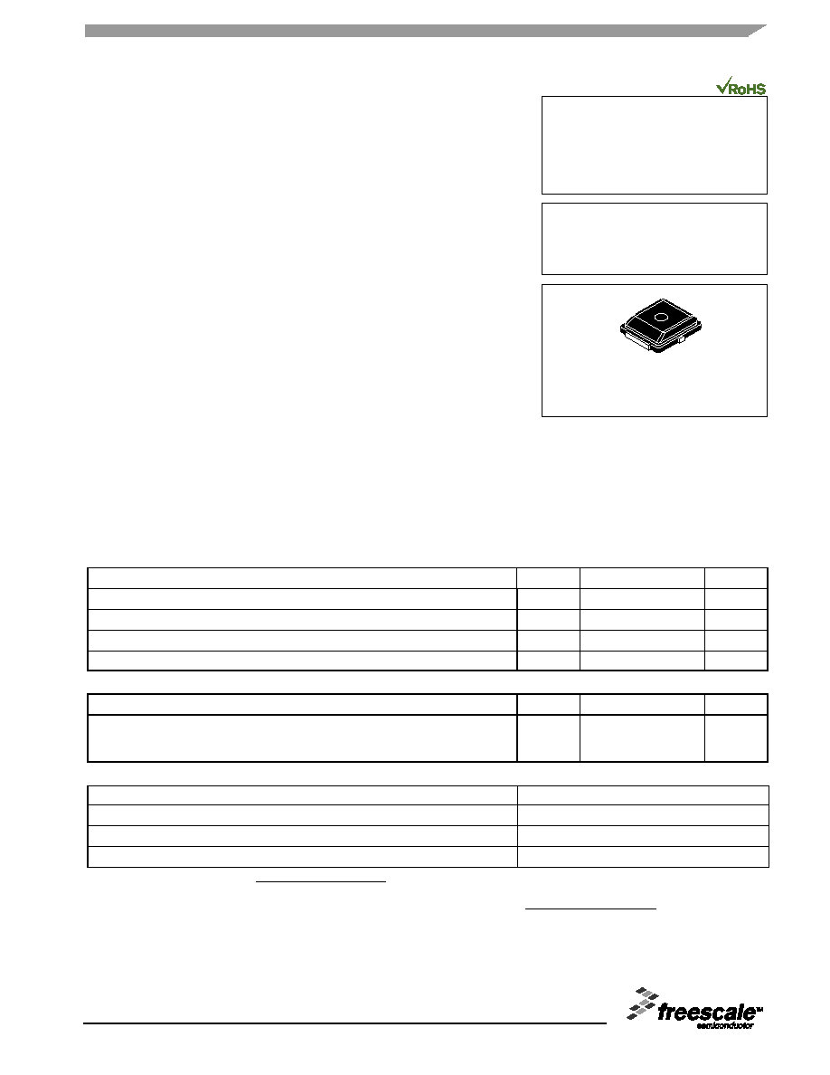
MW6S004NT1
1-2000 MHz, 4 W, 28 V
LATERAL N-CHANNEL
RF POWER MOSFET
CASE 466-03, STYLE 1
PLD 1.5
PLASTIC
Freescale Semiconductor, Inc., 2006. All rights reserved.
2
RF Device Data
Freescale Semiconductor
MW6S004NT1
Table 4. Moisture Sensitivity Level
Test Methodology
Rating
Package Peak Temperature
Unit
Per JESD 22-A113, IPC/JEDEC J-STD-020
3
260
∞C
Table 5. Electrical Characteristics
(T
C
= 25∞C unless otherwise noted)
Characteristic
Symbol
Min
Typ
Max
Unit
Off Characteristics
Zero Gate Voltage Drain Leakage Current
(V
DS
= 68 Vdc, V
GS
= 0 Vdc)
I
DSS
--
--
10
µAdc
Zero Gate Voltage Drain Leakage Current
(V
DS
= 28 Vdc, V
GS
= 0 Vdc)
I
DSS
--
--
10
µAdc
Gate-Source Leakage Current
(V
GS
= 5 Vdc, V
DS
= 0 Vdc)
I
GSS
--
--
500
nAdc
On Characteristics
Gate Threshold Voltage
(V
DS
= 10 Vdc, I
D
= 50 mAdc)
V
GS(th)
1
2.3
5
Vdc
Gate Quiescent Voltage
(1)
(V
DS
= 28 Vdc, I
D
= 50 mAdc, Measured in Functional Test)
V
GS(Q)
2
2.8
4
Vdc
Drain-Source On-Voltage
(V
GS
= 10 Vdc, I
D
= 50 mAdc)
V
DS(on)
--
0.27
0.37
Vdc
Dynamic Characteristics
Input Capacitance
(V
DS
= 28 Vdc ± 30 mV(rms)ac @ 1 MHz, V
GS
= 0 Vdc)
C
iss
--
30
--
pF
Reverse Transfer Capacitance
(V
DS
= 28 Vdc ± 30 mV(rms)ac @ 1 MHz, V
GS
= 0 Vdc)
C
rss
--
21
--
pF
Output Capacitance
(V
DS
= 28 Vdc ± 30 mV(rms)ac @ 1 MHz, V
GS
= 0 Vdc)
C
oss
--
25
--
pF
Functional Tests (In Freescale Test Fixture, 50 ohm system) V
DD
= 28 Vdc, I
DQ
= 50 mA, P
out
= 4 W PEP, f1 = 1960 MHz,
f2 = 1960.1 MHz, Two-Tone Test
Power Gain
G
ps
16.5
18
20
dB
Drain Efficiency
D
28
33
--
%
Intermodulation Distortion
IMD
--
-34
-28
dBc
Input Return Loss
IRL
--
-12
-10
dB
Typical Performances (In Freescale 900 MHz Demo Board, 50 ohm system) V
DD
= 28 Vdc, I
DQ
= 50 mA, P
out
= 4 W PEP,
f = 900 MHz, Two-Tone Test, 100 kHz Tone Spacing
Power Gain
G
ps
--
19
--
dB
Drain Efficiency
D
--
33
--
%
Intermodulation Distortion
IMD
--
-39
--
dBc
Input Return Loss
IRL
--
-12
--
dB
1. V
GG
=
11
/
10
x V
GS(Q)
. Parameter measured on Freescale Test Fixture, due to resistive divider network on the board.
Refer to Test Circuit Schematic.
MW6S004NT1
3
RF Device Data
Freescale Semiconductor
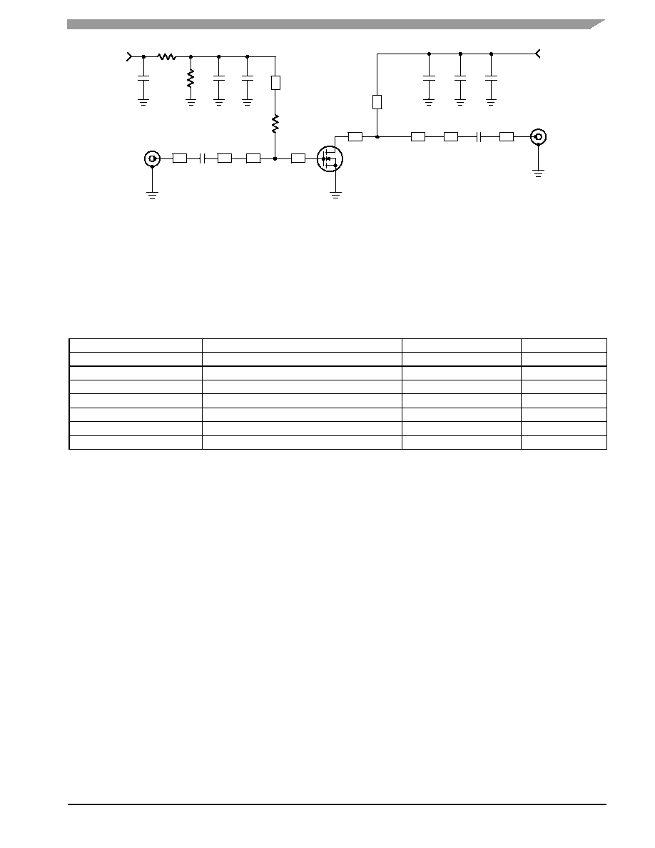
Figure 1. MW6S004NT1 Test Circuit Schematic
Z7
0.210 x 1.220 Microstrip
Z8
0.054 x 0.680 Microstrip
Z9
0.054 x 0.260 Microstrip
Z10
0.025 x 0.930 Microstrip
PCB
Arlon CuClad 250, 0.020,
r
= 2.5
Z1
0.054 x 0.430 Microstrip
Z2
0.054 x 0.137 Microstrip
Z3
0.580 x 0.420 Microstrip
Z4
0.580 x 0.100 Microstrip
Z5
0.025 x 0.680 Microstrip
Z6
0.210 x 0.100 Microstrip
RF
OUTPUT
V
BIAS
V
SUPPLY
RF
INPUT
DUT
Z1
C2
R1
C8
+
C1
C7
R2
Z5
R3
Z2
Z3
Z4
Z6
Z10
C3
C4
C5
Z7
Z8
C6
Z9
Table 6. MW6S004NT1 Test Circuit Component Designations and Values
Part
Description
Part Number
Manufacturer
C1
100 nF Chip Capacitor (1206)
CDR33BX104AKWS
Kemet
C2, C3, C6, C7
9.1 pF 600B Chip Capacitors
600B9R1CW
ATC
C4, C5
10 µF, 50 V Chip Capacitors
GRM55DR61H106KA88B
Murata
C8
10 µF, 35 V Tantalum Chip Capacitor
T490D106K035AS
Kemet
R1
1 k Chip Resistor (1206)
R2
10 k Chip Resistor (1206)
R3
10 Chip Resistor (1206)
4
RF Device Data
Freescale Semiconductor
MW6S004NT1
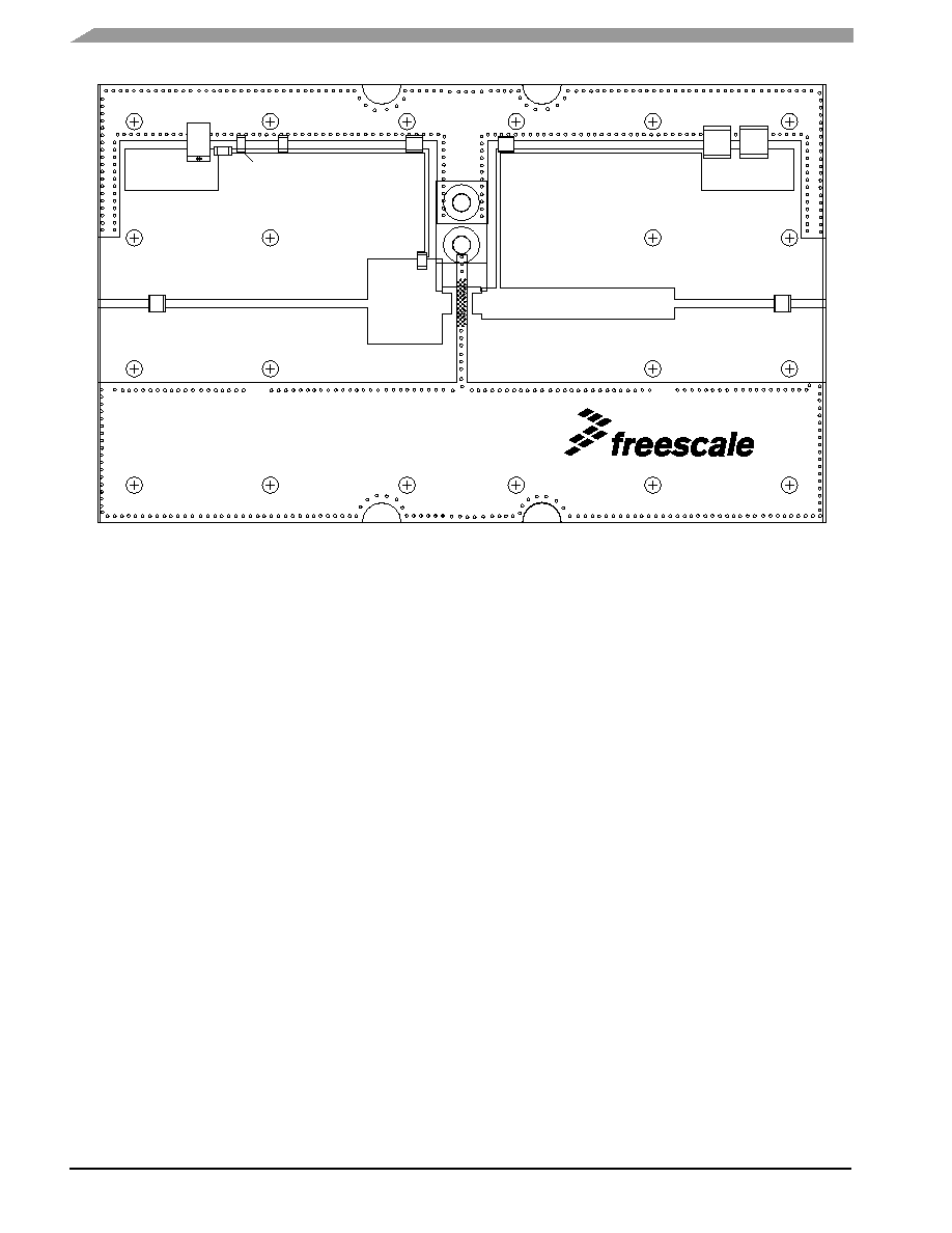
Figure 2. MW6S004NT1 Test Circuit Component Layout
25
C8
MW6S004N
Rev 3
R1
C1
R2
C7
C2
R3
C3
C4
C5
C6
MW6S004NT1
5
RF Device Data
Freescale Semiconductor
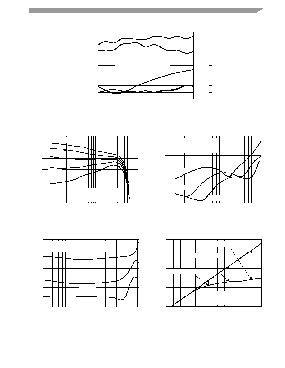
TYPICAL CHARACTERISTICS
G
ps
, POWER GAIN (dB)
IRL, INPUT RETURN LOSS (dB)
IM3 (dBc)
-28
-16
-20
-24
1990
1930
IRL
G
ps
f, FREQUENCY (MHz)
Figure 3. Two-Tone Wideband Performance
@ P
out
= 2 Watts Avg.
1980
1970
1960
1950
1940
18.4
18.2
-35
34
33
32
-31
-33
D
, DRAIN
EFFICIENCY (%)
D
18
17.8
17.6
17.2
16.4
16.8
17.4
-32
-30
31
-12
IM3
P
out
, OUTPUT POWER (WATTS) PEP
14
20
1
I
DQ
= 75 mA
19
17
16
10
20
Figure 4. Two-Tone Power Gain versus
Output Power
10
-80
-10
0.01
7th Order
V
DD
= 28 Vdc, I
DQ
= 50 mA
f1 = 1960 MHz, f2 = 1960.1 MHz
Two-Tone Measurements
5th Order
3rd Order
1
-20
-30
-40
-50
-60
P
out
, OUTPUT POWER (WATTS) PEP
Figure 5. Intermodulation Distortion Products
versus Output Power
IMD,
INTERMODULA
TION DIST
O
R
T
ION (dBc)
G
ps
, POWER GAIN (dB)
10
-60
-25
0.1
7th Order
TWO-TONE SPACING (MHz)
5th Order
3rd Order
-30
-35
-40
-45
-50
1
100
Figure 6. Intermodulation Distortion Products
versus Tone Spacing
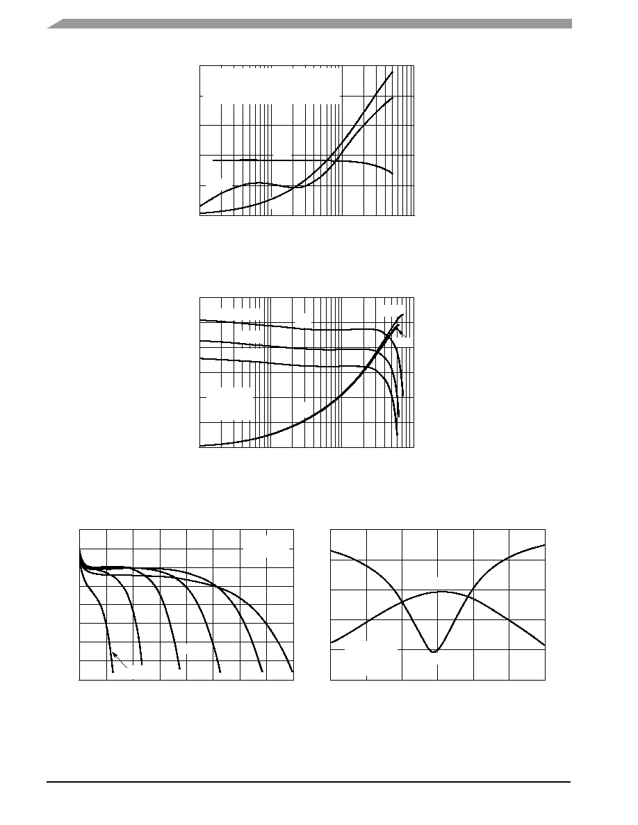
26
47
P3dB = 38.22 dBm (6.637 W)
P
in
, INPUT POWER (dBm)
V
DD
= 28 Vdc, I
DQ
= 50 mA
Pulsed CW, 8
µsec(on), 1 msec(off)
f = 1960 MHz
43
41
37
35
33
16
18
22
Actual
Ideal
24
14
Figure 7. Pulse CW Output Power versus
Input Power
IMD,
INTERMODULA
TION DIST
OR
TION (dBc)
P
out
, OUTPUT POWER (dBm)
18
50 mA
62.5 mA
P1dB = 37.61 dBm (5.768 W)
-55
0.01
V
DD
= 28 Vdc, P
out
= 2 W (Avg.)
I
DQ
= 50 mA, 100 kHz Tone Spacing
17
16.6
30
-34
-8
15
0.1
V
DD
= 28 Vdc
f1 = 1960 MHz, f2 = 1960.1 MHz
Two-Tone Measurements
37.5 mA
25 mA
-70
0.1
V
DD
= 28 Vdc, P
out
= 2 W (Avg.), I
DQ
= 50 mA
(f1 + f2)/2 = Center Frequency of 1960 MHz
45
39
20
P6dB = 38.73 dBm (7.465 W)
6
RF Device Data
Freescale Semiconductor
MW6S004NT1
TYPICAL CHARACTERISTICS
ACPR
(dB)
0
-70
P
out
, OUTPUT POWER (WATTS) AVG.
50
-20
40
-30
30
-40
20
-50
10
-60
0.01
1
10
G
ps
ACPR
Figure 8. Single-Carrier CDMA ACPR, Power Gain
and Drain Efficiency versus Output Power
10
14
20
0.01
0
60
T
C
= -30
_C
25
_C
-30
_C
1
19
18
17
16
40
30
20
10
P
out
, OUTPUT POWER (WATTS) CW
Figure 9. Power Gain and Drain Efficiency
versus CW Output Power
G
ps
, POWER GAIN (dB)
G
ps
P
out
, OUTPUT POWER (WATTS) CW
Figure 10. Power Gain versus Output Power
16 V
I
DQ
= 50 mA
f = 1960 MHz
V
DD
= 12 V
7
15
19
0
6
17
16
18
2
3
4
G
ps
, POWER GAIN (dB)
12
22
1800
-25
0
S21
f, FREQUENCY (MHz)
Figure 11. Broadband Frequency Response
S11
20
-5
18
16
-10
-15
14
-20
2100
2050
2000
1950
1900
1850
V
DD
= 28 Vdc
P
out
= 2 W CW
I
DQ
= 50 mA
S1
1
(
dB
)
S21 (dB)
85
_C
85
_C
8
5
1
20 V
V
DD
= 28 Vdc
I
DQ
= 50 mA
f = 1960 MHz
24 V
28 V
32 V
D
D
, DRAIN EFFICIENCY (%), G
ps
, POWER GAIN (dB)
D
,
DRAIN
EFFICIENCY (%)
0.1
V
DD
= 28 Vdc, I
DQ
= 50 mA
f = 1960 MHz, N-CDMA IS-95 (Pilot, Sync,
Paging, Traffic Codes 8 Through 13)
15
0.1
50
D
18.5
17.5
16.5
15.5
MW6S004NT1
7
RF Device Data
Freescale Semiconductor
TYPICAL CHARACTERISTICS
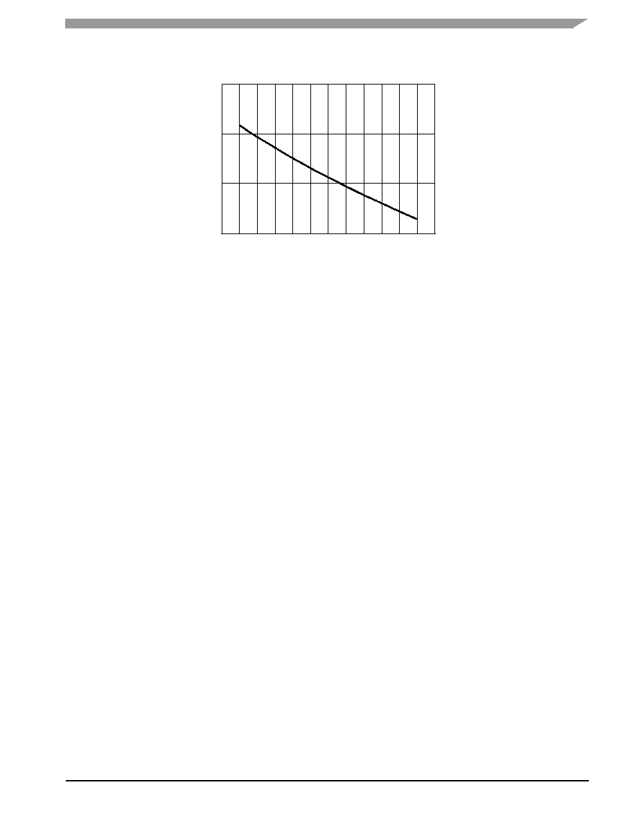
210
10
7
90
T
J
, JUNCTION TEMPERATURE (
∞C)
Figure 12. MTTF Factor versus Junction Temperature
This above graph displays calculated MTTF in hours x ampere
2
drain current. Life tests at elevated temperatures have correlated to
better than
±10% of the theoretical prediction for metal failure. Divide
MTTF factor by I
D
2
for MTTF in a particular application.
10
5
10
4
120
140
160
180 190
MTTF
F
ACT
OR (HOURS x AMPS
2
)
100
200
170
150
130
110
10
6
8
RF Device Data
Freescale Semiconductor
MW6S004NT1
f = 1930 MHz
Z
o
= 10
Z
load
Z
source
f = 1990 MHz
f = 1930 MHz
f = 1990 MHz
V
DD
= 28 Vdc, I
DQ
= 50 mA, P
out
= 4 W PEP
f
MHz
Z
source
W
Z
load
W
1930
1.96 - j5.34
8.78 + j6.96
1960
1.89 - j5.10
8.93 + j7.46
1990
1.82 - j4.85
9.11 + j7.97
Z
source
= Test circuit impedance as measured from
gate to ground.
Z
load
= Test circuit impedance as measured
from drain to ground.
Z source
Z load
Input
Matching
Network
Device
Under
Test
Output
Matching
Network
Figure 13. Series Equivalent Source and Load Impedance

MW6S004NT1
9
RF Device Data
Freescale Semiconductor
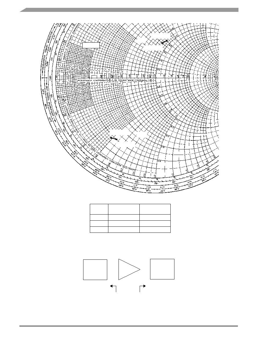
Table 7. Common Source Scattering Parameters (V
DD
= 28 V, 50 ohm system)
I
DQ
= 50 mA
f
MH
S
11
S
21
S
12
S
22
MHz
|S
11
|
|S
21
|
|S
12
|
|S
22
|
500
0.649
-116.340
7.902
105.420
0.056
-73.750
0.548
-33.570
550
0.695
-121.680
7.502
98.790
0.053
-80.570
0.593
-41.480
600
0.733
-126.560
7.111
92.380
0.049
-87.010
0.632
-48.890
650
0.770
-131.340
6.699
86.290
0.045
-93.280
0.669
-56.000
700
0.800
-135.740
6.302
80.450
0.041
-99.120
0.701
-62.810
750
0.827
-140.030
5.922
74.850
0.038
-104.850
0.727
-69.290
800
0.848
-143.950
5.552
69.630
0.035
-110.110
0.750
-75.350
850
0.866
-147.690
5.220
64.580
0.032
-115.220
0.770
-81.130
900
0.882
-151.140
4.891
59.970
0.029
-119.960
0.786
-86.570
950
0.895
-154.560
4.597
55.490
0.026
-124.790
0.800
-91.730
1000
0.907
-157.590
4.315
51.240
0.024
-129.090
0.813
-96.660
1050
0.916
-160.540
4.060
47.170
0.022
-133.370
0.824
-101.340
1100
0.923
-163.310
3.819
43.340
0.020
-137.460
0.833
-105.790
1150
0.929
-165.930
3.601
39.650
0.018
-141.440
0.840
-110.050
1200
0.935
-168.430
3.398
36.110
0.017
-145.330
0.847
-114.170
1250
0.938
-170.770
3.210
32.740
0.015
-149.540
0.851
-118.060
1300
0.942
-173.030
3.036
29.490
0.014
-153.430
0.856
-121.880
1350
0.945
-175.140
2.875
26.360
0.013
-157.460
0.859
-125.520
1400
0.948
-177.170
2.728
23.330
0.012
-161.910
0.863
-129.020
1450
0.951
-179.090
2.590
20.440
0.011
-166.180
0.866
-132.390
1500
0.953
179.030
2.464
17.640
0.010
-170.630
0.869
-135.650
1550
0.954
177.270
2.347
14.920
0.009
-174.890
0.872
-138.760
1600
0.955
175.570
2.240
12.320
0.008
179.950
0.875
-141.750
1650
0.956
173.980
2.139
9.740
0.008
173.920
0.877
-144.650
1700
0.957
172.350
2.047
7.250
0.007
167.710
0.880
-147.480
1750
0.957
170.800
1.958
4.810
0.007
161.810
0.882
-150.180
1800
0.958
169.340
1.879
2.440
0.006
155.370
0.884
-152.760
1850
0.959
167.920
1.806
0.260
0.006
148.940
0.886
-155.230
1900
0.959
166.510
1.736
-1.980
0.005
142.630
0.887
-157.580
1950
0.960
165.200
1.668
-4.310
0.005
136.740
0.888
-160.050
2000
0.959
163.800
1.611
-6.240
0.005
129.910
0.890
-162.070
2050
0.959
162.420
1.555
-8.290
0.005
123.810
0.891
-164.190
2100
0.958
161.170
1.504
-10.270
0.005
118.200
0.892
-166.140
2150
0.958
159.840
1.456
-12.210
0.005
112.740
0.893
-168.060
2200
0.957
158.560
1.412
-14.130
0.005
108.460
0.894
-169.840
2250
0.957
157.160
1.372
-16.010
0.005
103.840
0.896
-171.610
2300
0.955
155.870
1.334
-17.870
0.005
99.310
0.896
-173.260
2350
0.954
154.510
1.300
-19.700
0.005
95.360
0.897
-174.830
2400
0.953
153.120
1.268
-21.510
0.005
91.030
0.898
-176.390
2450
0.953
151.730
1.238
-23.250
0.005
87.460
0.899
-177.840

10
RF Device Data
Freescale Semiconductor
MW6S004NT1
Table 7. Common Source Scattering Parameters (V
DD
= 28 V, 50 ohm system) (continued)
I
DQ
= 50 mA
f
MH
S
11
S
21
S
12
S
22
MHz
|S
11
|
|S
21
|
|S
12
|
|S
22
|
2500
0.952
150.340
1.211
-25.120
0.006
84.160
0.899
-179.270
2550
0.950
149.010
1.187
-26.920
0.006
80.780
0.897
179.420
2600
0.949
147.380
1.166
-28.650
0.006
77.880
0.897
178.120
2650
0.948
145.920
1.144
-30.420
0.007
74.670
0.898
176.840
2700
0.944
144.200
1.121
-32.310
0.007
71.360
0.896
175.480
2750
0.944
142.790
1.105
-34.230
0.007
67.980
0.897
174.060
2800
0.943
141.020
1.088
-36.000
0.007
63.950
0.897
172.930
2850
0.941
139.410
1.073
-37.870
0.007
61.230
0.896
171.630
2900
0.940
137.640
1.058
-39.760
0.008
59.810
0.896
170.330
2950
0.938
135.900
1.045
-41.680
0.008
58.280
0.896
169.040
3000
0.937
133.860
1.032
-43.610
0.008
56.740
0.895
167.510
MW6S004NT1
11
RF Device Data
Freescale Semiconductor
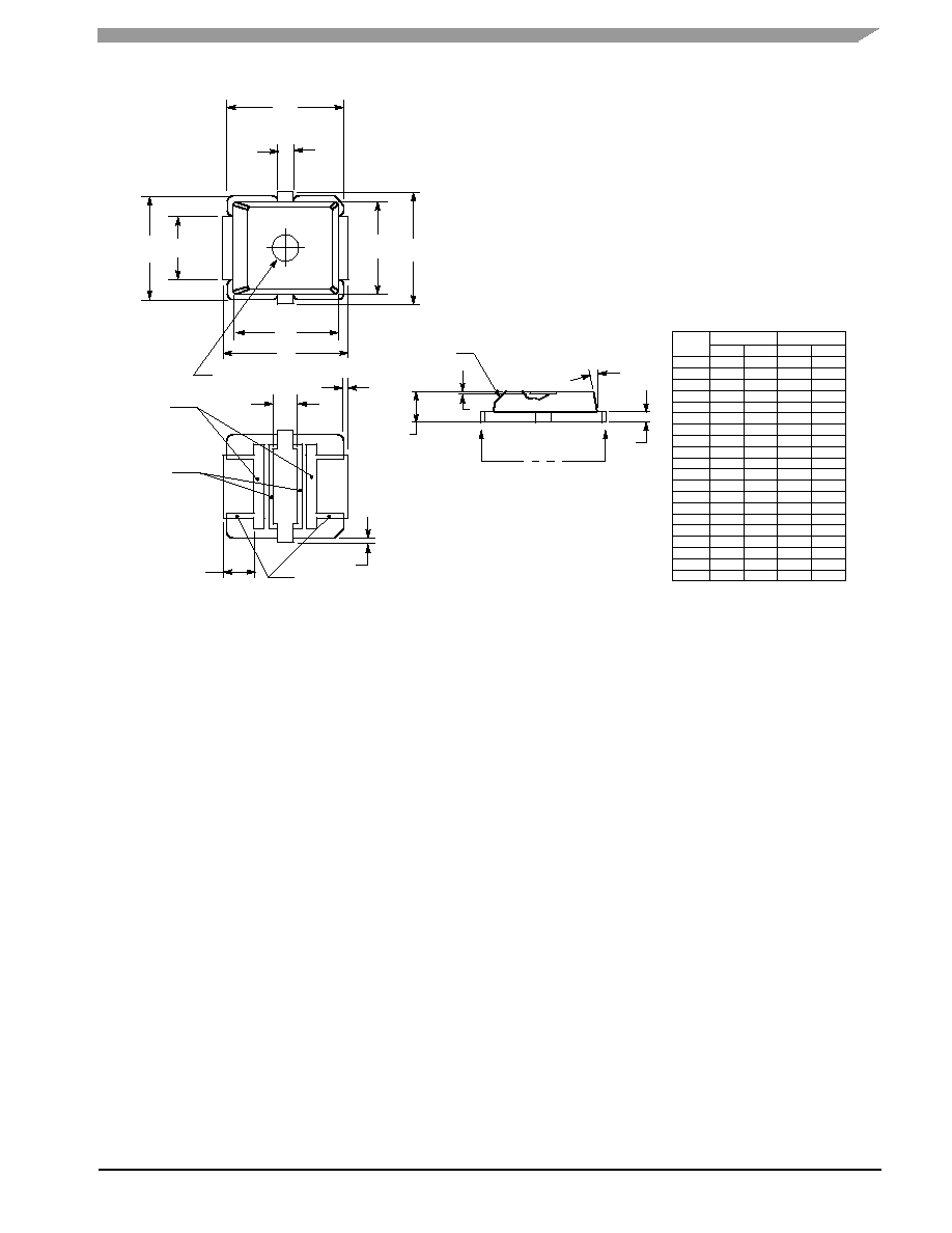
PACKAGE DIMENSIONS
CASE 466-03
ISSUE D
NOTES:
1. INTERPRET DIMENSIONS AND TOLERANCES
PER ASME Y14.5M, 1984.
2. CONTROLLING DIMENSION: INCH
3. RESIN BLEED/FLASH ALLOWABLE IN ZONE V, W,
AND X.
DIM
MIN
MAX
MIN
MAX
MILLIMETERS
INCHES
A
0.255
0.265
6.48
6.73
B
0.225
0.235
5.72
5.97
C
0.065
0.072
1.65
1.83
D
0.130
0.150
3.30
3.81
E
0.021
0.026
0.53
0.66
F
0.026
0.044
0.66
1.12
G
0.050
0.070
1.27
1.78
H
0.045
0.063
1.14
1.60
K
0.273
0.285
6.93
7.24
L
0.245
0.255
6.22
6.48
N
0.230
0.240
5.84
6.10
P
0.000
0.008
0.00
0.20
Q
0.055
0.063
1.40
1.60
R
0.200
0.210
5.08
5.33
S
0.006
0.012
0.15
0.31
U
0.006
0.012
0.15
0.31
ZONE V
0.000
0.021
0.00
0.53
ZONE W
0.000
0.010
0.00
0.25
ZONE X
0.000
0.010
0.00
0.25
STYLE 1:
PIN 1. DRAIN
2. GATE
3. SOURCE
4. SOURCE
J
0.160
0.180
4.06
4.57
………
………
………
………
………
………
………
………
………
………
……
……
……
……
……
A
B
D
F
L
R
3
4
2
1
K
N
ZONE V
ZONE W
ZONE X
G
S
H
U
_
10 DRAFT
P
C
E
0.35 (0.89) X 45 5
"
Y
Y
Q
VIEW Y-Y
_
_
4
2
1
3
PLASTIC
PLD 1.5

12
RF Device Data
Freescale Semiconductor
MW6S004NT1
Information in this document is provided solely to enable system and software
implementers to use Freescale Semiconductor products. There are no express or
implied copyright licenses granted hereunder to design or fabricate any integrated
circuits or integrated circuits based on the information in this document.
Freescale Semiconductor reserves the right to make changes without further notice to
any products herein. Freescale Semiconductor makes no warranty, representation or
guarantee regarding the suitability of its products for any particular purpose, nor does
Freescale Semiconductor assume any liability arising out of the application or use of
any product or circuit, and specifically disclaims any and all liability, including without
limitation consequential or incidental damages. "Typical" parameters that may be
provided in Freescale Semiconductor data sheets and/or specifications can and do
vary in different applications and actual performance may vary over time. All operating
parameters, including "Typicals", must be validated for each customer application by
customer's technical experts. Freescale Semiconductor does not convey any license
under its patent rights nor the rights of others. Freescale Semiconductor products are
not designed, intended, or authorized for use as components in systems intended for
surgical implant into the body, or other applications intended to support or sustain life,
or for any other application in which the failure of the Freescale Semiconductor product
could create a situation where personal injury or death may occur. Should Buyer
purchase or use Freescale Semiconductor products for any such unintended or
unauthorized application, Buyer shall indemnify and hold Freescale Semiconductor
and its officers, employees, subsidiaries, affiliates, and distributors harmless against all
claims, costs, damages, and expenses, and reasonable attorney fees arising out of,
directly or indirectly, any claim of personal injury or death associated with such
unintended or unauthorized use, even if such claim alleges that Freescale
Semiconductor was negligent regarding the design or manufacture of the part.
Freescalet and the Freescale logo are trademarks of Freescale Semiconductor, Inc.
All other product or service names are the property of their respective owners.
Freescale Semiconductor, Inc. 2006. All rights reserved.
How to Reach Us:
Home Page:
www.freescale.com
E-mail:
support@freescale.com
USA/Europe or Locations Not Listed:
Freescale Semiconductor
Technical Information Center, CH370
1300 N. Alma School Road
Chandler, Arizona 85224
+1-800-521-6274 or +1-480-768-2130
support@freescale.com
Europe, Middle East, and Africa:
Freescale Halbleiter Deutschland GmbH
Technical Information Center
Schatzbogen 7
81829 Muenchen, Germany
+44 1296 380 456 (English)
+46 8 52200080 (English)
+49 89 92103 559 (German)
+33 1 69 35 48 48 (French)
support@freescale.com
Japan:
Freescale Semiconductor Japan Ltd.
Headquarters
ARCO Tower 15F
1-8-1, Shimo-Meguro, Meguro-ku,
Tokyo 153-0064
Japan
0120 191014 or +81 3 5437 9125
support.japan@freescale.com
Asia/Pacific:
Freescale Semiconductor Hong Kong Ltd.
Technical Information Center
2 Dai King Street
Tai Po Industrial Estate
Tai Po, N.T., Hong Kong
+800 2666 8080
support.asia@freescale.com
For Literature Requests Only:
Freescale Semiconductor Literature Distribution Center
P.O. Box 5405
Denver, Colorado 80217
1-800-441-2447 or 303-675-2140
Fax: 303-675-2150
LDCForFreescaleSemiconductor@hibbertgroup.com
Document Number: MW6S004N
Rev. 1, 4/2006