
MW6S010NR1 MW6S010GNR1 MW6S010MR1 MW6S010GMR1
1
RF Device Data
Freescale Semiconductor
RF Power Field Effect Transistor
N-Channel Enhancement-Mode Lateral MOSFETs
Designed for Class A or Class AB base station applications with frequencies
up to 1500 MHz. Suitable for analog and digital modulation and multicarrier
amplifier applications.
∑ Typical Two-Tone Performance @ 960 MHz, V
DD
= 28 Volts, I
DQ
=
125 mA, P
out
= 10 Watts PEP
Power Gain -- 18 dB
Drain Efficiency -- 32%
IMD -- -37 dBc
∑ Capable of Handling 10:1 VSWR, @ 28 Vdc, 960 MHz, 10 Watts CW
Output Power
∑ Characterized with Series Equivalent Large-Signal Impedance Parameters
∑ On-Chip RF Feedback for Broadband Stability
∑ Qualified Up to a Maximum of 32 V
DD
Operation
∑ Integrated ESD Protection
∑ N Suffix Indicates Lead-Free Terminations
∑ 200∞C Capable Plastic Package
∑ In Tape and Reel. R1 Suffix = 500 Units per 24 mm, 13 inch Reel.
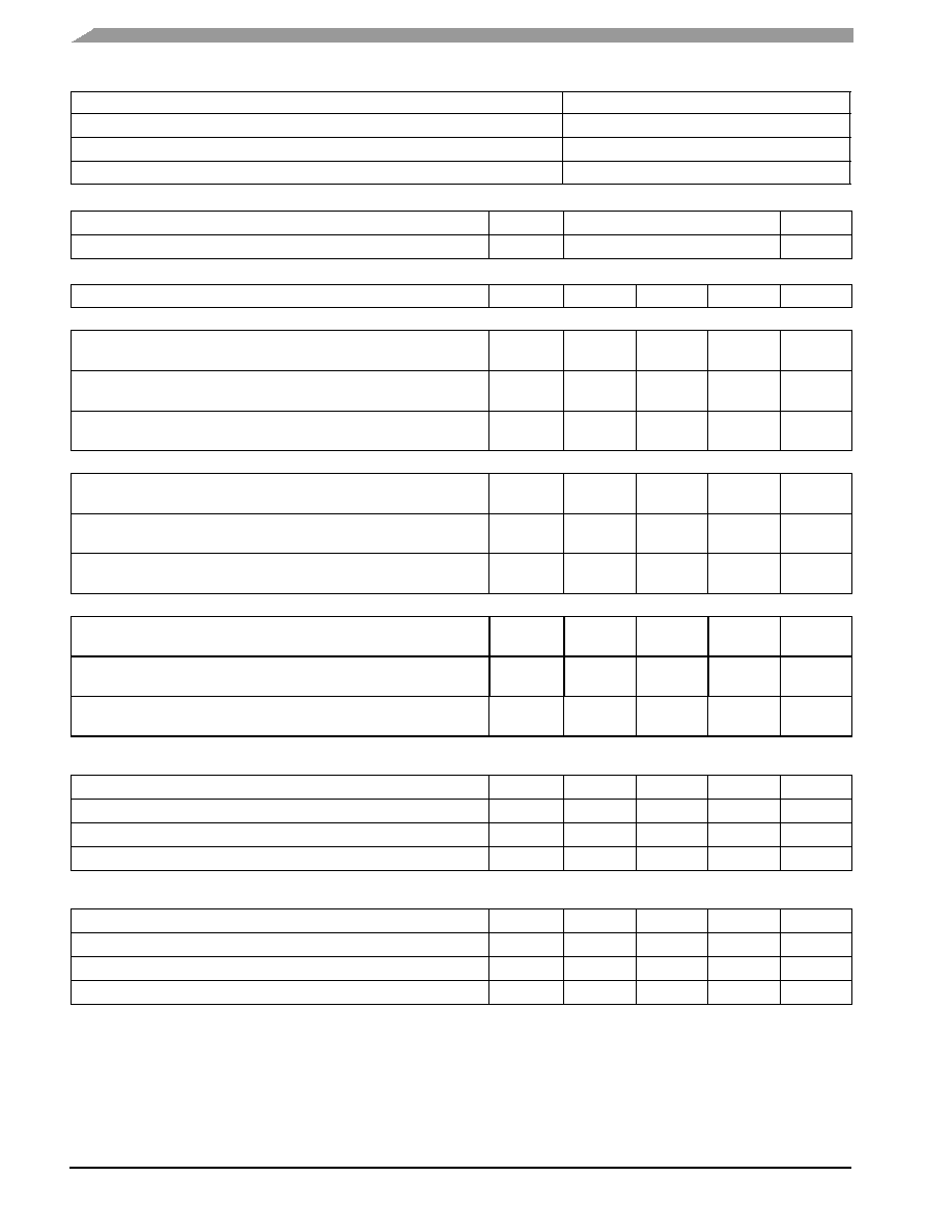
Table 1. Maximum Ratings
Rating
Symbol
Value
Unit
Drain-Source Voltage
V
DSS
-0.5, +68
Vdc
Gate-Source Voltage
V
GS
-0.5, +12
Vdc
Total Device Dissipation @ T
C
= 25∞C
Derate above 25∞C
P
D
61.4
0.35
W
W/∞C
Storage Temperature Range
T
stg
- 65 to +175
∞C
Operating Junction Temperature
T
J
200
∞C
Table 2. Thermal Characteristics
Characteristic
Symbol
Value
(1.2)
Unit
Thermal Resistance, Junction to Case
Case Temperature 80∞C, 10 W PEP
R
JC
2.85
∞C/W
1. MTTF calculator available at http://www.freescale.com/rf. Select Tools/Software/Application Software/Calculators to access
the MTTF calculators by product.
2. Refer to AN1955, Thermal Measurement Methodology of RF Power Amplifiers. Go to http://www.freescale.com/rf.
Select Documentation/Application Notes - AN1955.
NOTE - CAUTION - MOS devices are susceptible to damage from electrostatic charge. Reasonable precautions in handling and
packaging MOS devices should be observed.
Document Number: MW6S010
Rev. 1, 5/2005
Freescale Semiconductor
Technical Data
MW6S010NR1
MW6S010GNR1
MW6S010MR1
MW6S010GMR1
450-1500 MHz, 10 W, 28 V
LATERAL N-CHANNEL
BROADBAND RF POWER MOSFETs
CASE 1265-08, STYLE 1
TO-270-2
PLASTIC
MW6S010NR1(MR1)
CASE 1265A-02, STYLE 1
TO-270-2 GULL
PLASTIC
MW6S010GNR1(GMR1)
Freescale Semiconductor, Inc., 2005. All rights reserved.
2
RF Device Data
Freescale Semiconductor
MW6S010NR1 MW6S010GNR1 MW6S010MR1 MW6S010GMR1
Table 3. ESD Protection Characteristics
Test Methodology
Class
Human Body Model (per JESD22-A114)
1A
Machine Model (per EIA/JESD22-A115)
A
Charge Device Model (per JESD22-C101)
III
Table 4. Moisture Sensitivity Level
Test Methodology
Rating
Package Peak Temperature
Unit
Per JESD 22-A113, IPC/JEDEC J-STD-020
1
260
∞C
Table 5. Electrical Characteristics
(T
C
= 25∞C unless otherwise noted)
Characteristic
Symbol
Min
Typ
Max
Unit
Off Characteristics
Zero Gate Voltage Drain Leakage Current
(V
DS
= 68
Vdc, V
GS
= 0 Vdc)
I
DSS
--
--
10
µAdc
Zero Gate Voltage Drain Leakage Current
(V
DS
= 28 Vdc, V
GS
= 0 Vdc)
I
DSS
--
--
1
µAdc
Gate-Source Leakage Current
(V
GS
= 5 Vdc, V
DS
= 0 Vdc)
I
GSS
--
--
1
µAdc
On Characteristics
Gate Threshold Voltage
(V
DS
= 10 Vdc, I
D
= 100 µAdc)
V
GS(th)
1.5
2.3
3
Vdc
Gate Quiescent Voltage
(V
DS
= 28 Vdc, I
D
= 125 mAdc)
V
GS(Q)
--
3.1
--
Vdc
Drain-Source On-Voltage
(V
GS
= 10 Vdc, I
D
= 0.3 Adc)
V
DS(on)
--
0.27
0.35
Vdc
Dynamic Characteristics
Input Capacitance
(V
DS
= 28 Vdc ± 30 mV(rms)ac @ 1 MHz, V
GS
= 0 Vdc)
C
iss
--
23
--
pF
Output Capacitance
(V
DS
= 28 Vdc ± 30 mV(rms)ac @ 1 MHz, V
GS
= 0 Vdc)
C
oss
--
10
--
pF
Reverse Transfer Capacitance
(V
DS
= 28 Vdc ± 30 mV(rms)ac @ 1 MHz, V
GS
= 0 Vdc)
C
rss
--
0.32
--
pF
Functional Tests (In Freescale Test Fixture, 50 ohm system) V
DD
= 28 Vdc, I
DQ
= 125 mA, P
out
= 10 W PEP, f = 960 MHz,
Two-Tone Test, 100 kHz Tone Spacing
Power Gain
G
ps
17.5
18
20.5
dB
Drain Efficiency
D
31
32
--
%
Intermodulation Distortion
IMD
--
-37
-33
dBc
Input Return Loss
IRL
--
-18
-10
dB
Typical
Performances (In Freescale 450 MHz Demo Board, 50 hm system) V
DD
= 28 Vdc, I
DQ
= 150 mA, P
out
= 10 W PEP,
420 MHz<Frequency<470 MHz, Two-Tone Test, 100 kHz Tone Spacing
Power Gain
G
ps
--
20
--
dB
Drain Efficiency
D
--
33
--
%
Intermodulation Distortion
IMD
--
-40
--
dBc
Input Return Loss
IRL
--
-10
--
dB
MW6S010NR1 MW6S010GNR1 MW6S010MR1 MW6S010GMR1
3
RF Device Data
Freescale Semiconductor
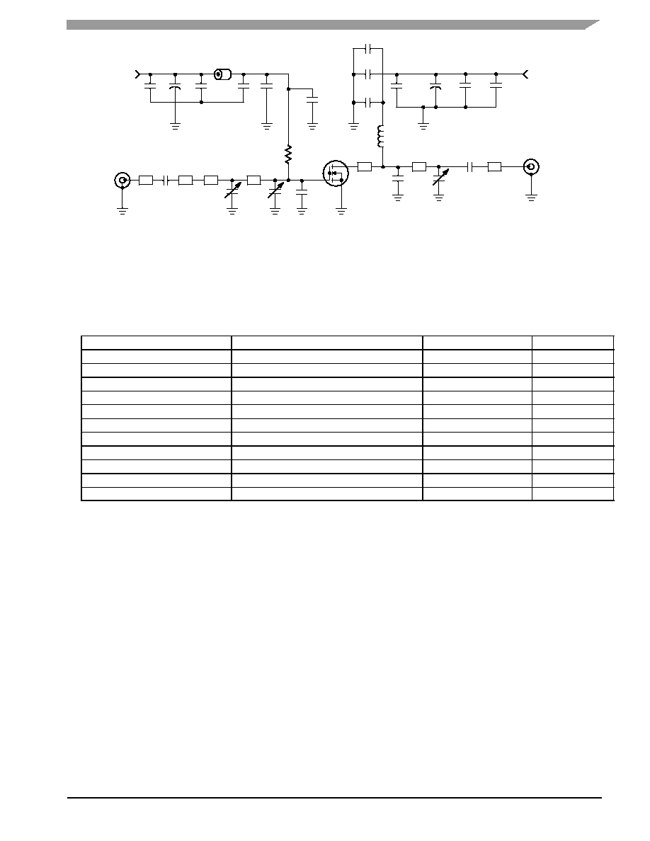
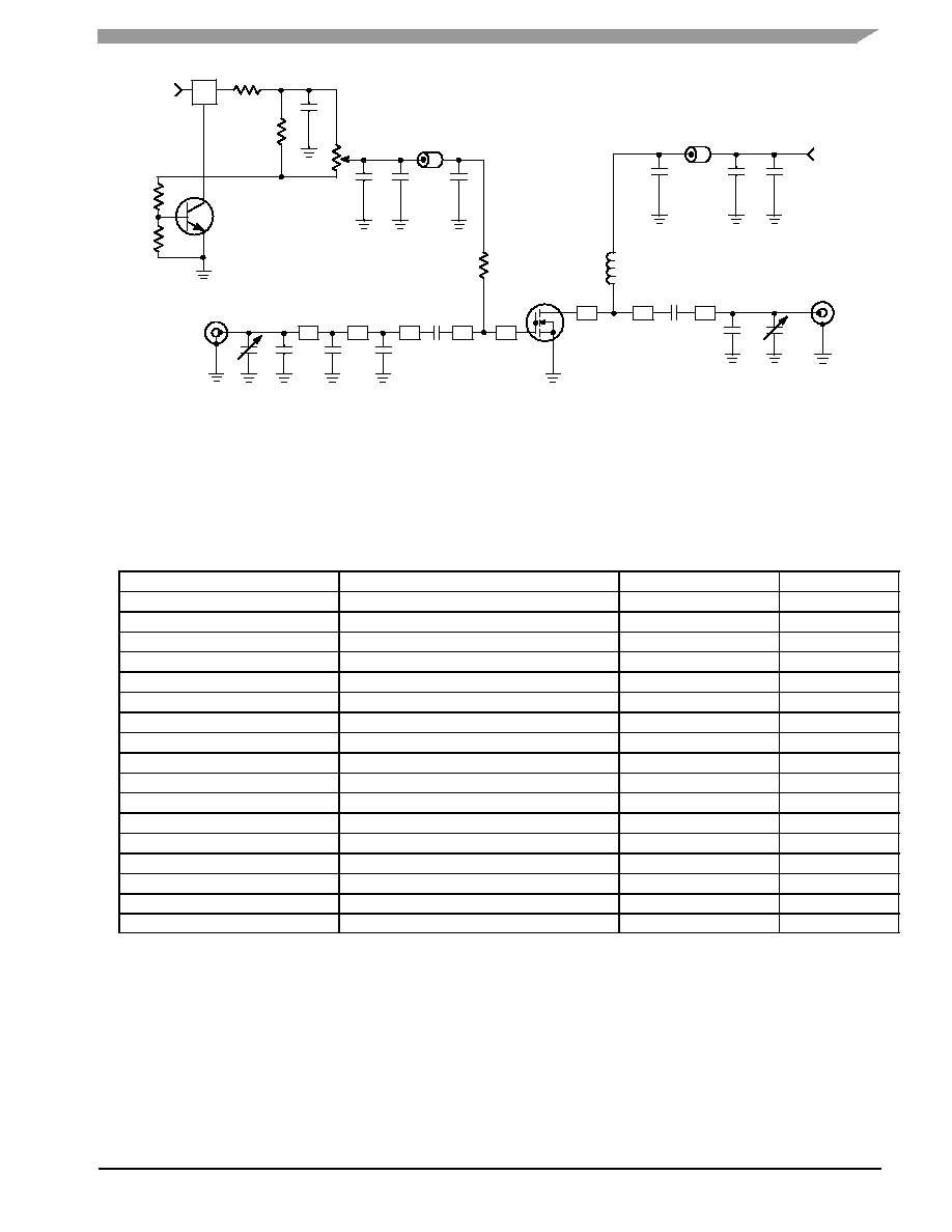
Figure 1. MW6S010NR1(GNR1/MR1/GMR1) Test Circuit Schematic -- 900 MHz
C9
C2
+
RF
OUTPUT
C5
V
BIAS
C3
+
V
SUPPLY
RF
INPUT
Z1
C1
Z2
Z3
Z4
C8
R1
DUT
C4
B1
C6
C7
C10
Z5
L1
C14
Z6
C17
C20
Z7
C11
C12
C13
C15
C16
+
C18
+
C19
+
Z5
0.313 x 0.902 Microstrip
Z6
0.073 x 1.080 Microstrip
Z7
0.073 x 0.314 Microstrip
PCB
Rogers ULTRALAM 2000, 0.031,
r
= 2.55
Z1
0.073 x 0.223 Microstrip
Z2
0.112 x 0.070 Microstrip
Z3
0.213 x 0.500 Microstrip
Z4
0.313 x 1.503 Microstrip
Table 6. MW6S010NR1(GNR1/MR1/GMR1) Test Circuit Component Designations and Values -- 900 MHz
Part
Description
Part Number
Manufacturer
B1
Ferrite Bead
2743019447
Fair-Rite
C1, C6, C11, C20
47 pF Chip Capacitors
100B470JP500X
ATC
C2, C18, C19
22 µF, 35 V Tantalum Capacitors
T491D226K035AS
Kemet
C3, C16
220 µF, 63 V Electrolytic Capacitors, Radial
13668221
Phillips
C4, C15
0.1 µF Chip Capacitors
CDR33BX104AKWS
Kemet
C5, C8, C17
0.8-8.0 pF Variable Capacitors, Gigatrim
272915L
Johanson
C7, C12
24 pF Chip Capacitors
100B240JP500X
ATC
C9, C10, C13
6.8 pF Chip Capacitors
100B6R8JP500X
ATC
C14
7.5 pF Chip Capacitor
100B7R5JP500X
ATC
L1
12.5 nH Inductor
A04T-5
Coilcraft
R1
1 k Chip Resistor
CRCW12061001F100
Vishay -Dale
4
RF Device Data
Freescale Semiconductor
MW6S010NR1 MW6S010GNR1 MW6S010MR1 MW6S010GMR1
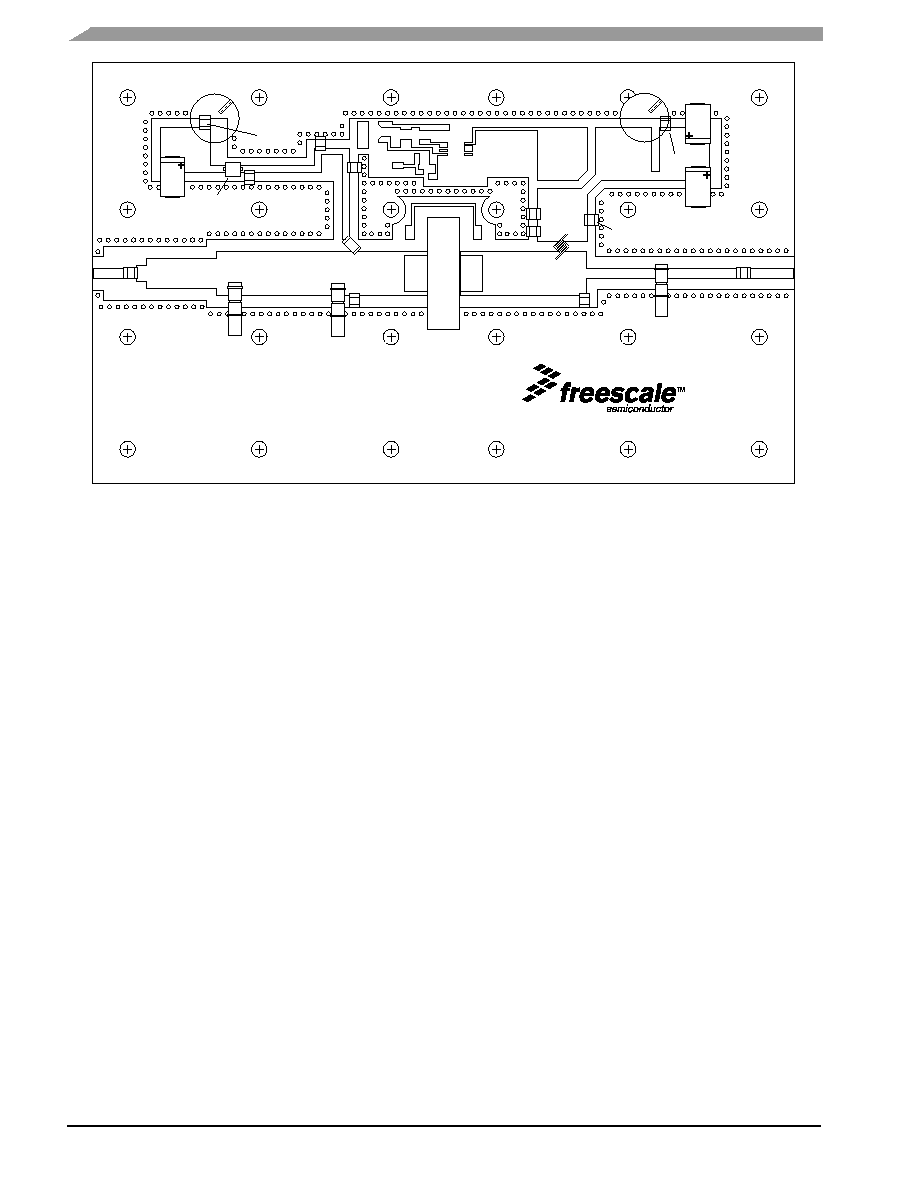
Figure 2. MW6S010NR1(GNR1/MR1/GMR1) Test Circuit Component Layout -- 900 MHz
C3
MW6S010N
C4
C7
C10
C6
B1
C2
C1
C5
C8
C9
R1
L1
C16
C18
C19
C15
C12
C11
C13
C14
C17
C20
MW6S010NR1 MW6S010GNR1 MW6S010MR1 MW6S010GMR1
5
RF Device Data
Freescale Semiconductor
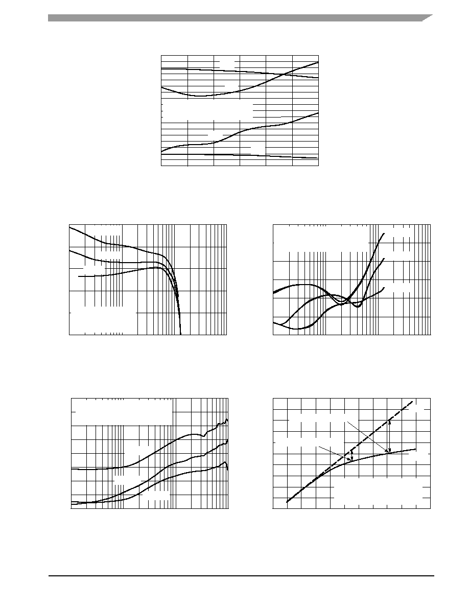
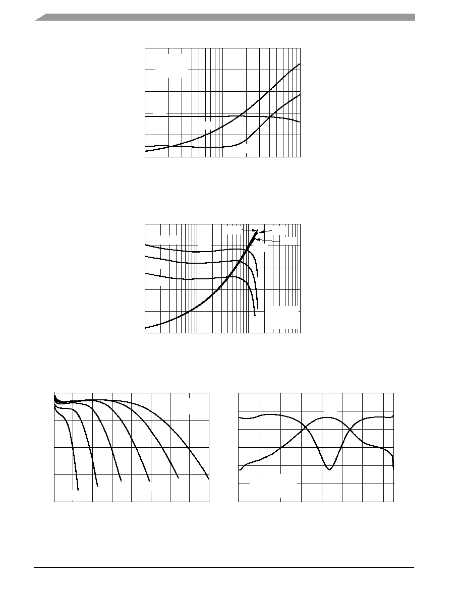
TYPICAL CHARACTERISTICS
-- 900 MHz
970
16
48
910
-26
-8
IRL
G
ps
IMD
f, FREQUENCY (MHz)
V
DD
= 28 Vdc, P
out
= 10 W (Avg.)
I
DQ
= 125 mA, 100 kHz Tone Spacing
44
-10
40
-12
36
-14
32
-16
28
-18
24
-20
20
-22
930
950
960
Figure 3. Two-Tone Wideband Performance
@ P
out
= 10 Watts
P
out
, OUTPUT POWER (WATTS) AVG.
15
20
1
I
DQ
= 190 mA
V
DD
= 28 Vdc, f = 945 MHz
Two -Tone Measurements
100 kHz Tone Spacing
19
17
16
10
100
Figure 4. Two-Tone Power Gain versus
Output Power
100
-70
-10
0.1
7th Order
V
DD
= 28 Vdc, I
DQ
= 125 mA
f = 945 MHz, Two -Tone Measurements
100 kHz Tone Spacing
5th Order
3rd Order
1
10
-20
-30
-40
-50
-60
P
out
, OUTPUT POWER (WATTS) AVG.
Figure 5. Intermodulation Distortion Products
versus Output Power
IMD,
INTERMODULA
TION
DIST
ORTION
(dBc)
G
ps
, POWER GAIN (dB)
IRL, INPUT RETURN LOSS (dB)
IMD, INTERMODULA
TION
DIST
ORTION
(dBc)
10
-55
-15
0.1
7th Order
TWO -TONE SPACING (MHz)
V
DD
= 28 Vdc, P
out
= 10 W (Avg.)
I
DQ
= 125 mA, Two -Tone Measurements
Center Frequency = 945 MHz
5th Order
3rd Order
-20
-25
-30
-35
-40
1
100
Figure 6. Intermodulation Distortion Products
versus Tone Spacing
29
48
P3dB = 43.14 dBm (20.61 W)
P
in
, INPUT POWER (dBm)
V
DD
= 28 Vdc, I
DQ
= 125 mA
Pulsed CW, 8
µsec(on), 1 msec(off)
Center Frequency = 945 MHz
46
44
42
40
38
21
23
25
Actual
Ideal
27
19
Figure 7. Pulse CW Output Power versus
Input Power
IMD,
INTERMODULA
TION
DIST
ORTION
(dBc)
P
out
, OUTPUT POWER (dBm)
920
940
18
90 mA
125 mA
P1dB = 42.23 dBm (16.71 W)
-50
-45
-24
0.1
D
, DRAIN EFFICIENCY (%), G
ps
, POWER GAIN (dB)
D
6
RF Device Data
Freescale Semiconductor
MW6S010NR1 MW6S010GNR1 MW6S010MR1 MW6S010GMR1
TYPICAL CHARACTERISTICS
-- 900 MHz
ACPR
(dBc)
0
-60
P
out
, OUTPUT POWER (WATTS) AVG.
50
-10
40
-20
30
-30
20
-40
10
-50
0.1
1
10
G
ps
ACPR
V
DD
= 28 Vdc
I
DQ
= 125 mA
f = 945 MHz
Figure 8. Single-Carrier CDMA ACPR, Power
Gain and Power Added Efficiency
versus Output Power
100
15
20
0.1
0
50
T
C
= -30
_C
25
_C
-30
_C
10
1
19
18
17
16
40
30
20
10
P
out
, OUTPUT POWER (WATTS) CW
Figure 9. Power Gain and Power Added
Efficiency versus Output Power
G
ps
, POWER GAIN (dB)
G
ps
P
out
, OUTPUT POWER (WATTS) CW
Figure 10. Power Gain versus Output Power
16 V
I
DQ
= 125 mA
f = 945 MHz
V
DD
= 12 V
14
15
19
0
12
17
16
18
4
6
8
G
ps
, POWER GAIN (dB)
0
24
500
-25
5
S21
f, FREQUENCY (MHz)
Figure 11. Broadband Frequency Response
S11
20
0
16
-5
12
-10
8
-15
4
-20
1200
1100
1000
900
800
700
600
V
DD
= 28 Vdc
P
out
= 10 W CW
I
DQ
= 125 mA
S1
1 (dB)
S21 (dB)
85
_C
25
_C
85
_C
16
10
2
20 V
V
DD
= 28 Vdc
I
DQ
= 125 mA
f = 945 MHz
24 V
28 V
32 V
D
D
, DRAIN EFFICIENCY (%), G
ps
, POWER GAIN (dB)
D
D
,
DRAIN
EFFICIENCY (%)
MW6S010NR1 MW6S010GNR1 MW6S010MR1 MW6S010GMR1
7
RF Device Data
Freescale Semiconductor
TYPICAL CHARACTERISTICS
210
10
8
90
T
J
, JUNCTION TEMPERATURE (
∞C)
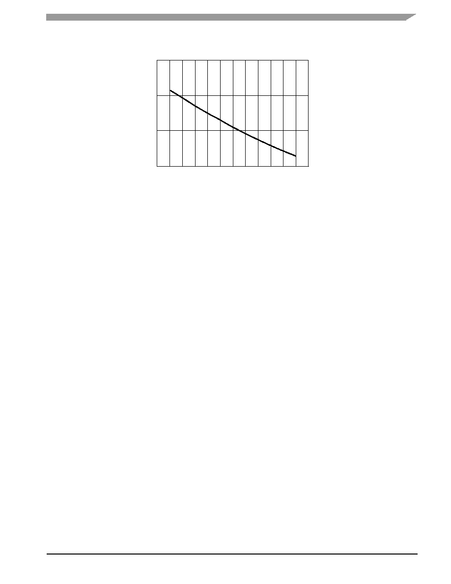
Figure 12. MTTF Factor versus Junction Temperature
This above graph displays calculated MTTF in hours x ampere
2
drain current. Life tests at elevated temperatures have correlated to
better than
±10% of the theoretical prediction for metal failure. Divide
MTTF factor by I
D
2
for MTTF in a particular application.
10
7
10
6
10
5
120
140
160
180 190
MTTF
F
ACT
OR (HOURS x AMPS
2
)
100
200
170
150
130
110
8
RF Device Data
Freescale Semiconductor
MW6S010NR1 MW6S010GNR1 MW6S010MR1 MW6S010GMR1
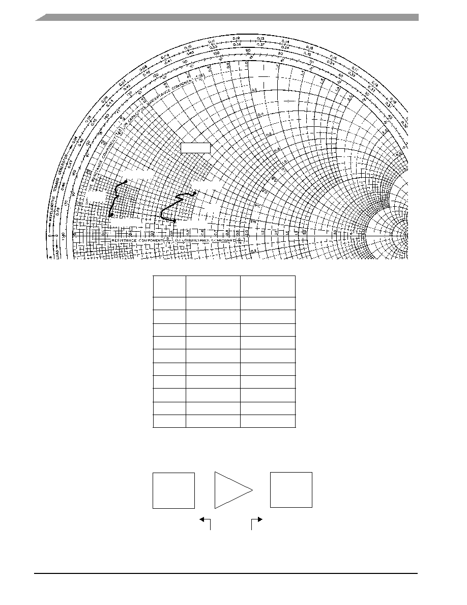
f
MHz
Z
source
Z
load
800
820
840
3.1 + j1.9
2.7 + j2.2
2.8 + j1.7
10.1 + j2.3
8.3 + j2.5
8.2 + j3.3
V
DD
= 28 Vdc, I
DQ
= 125 mA, P
out
= 10 W PEP
860
880
900
3.1 + j3.4
2.9 + j3.7
3.3 + j3.8
9.8 + j4.8
10.6 + j5.6
9.5 + j5.5
920
940
960
2.8 + j4.4
3.2 + j4.9
3.0 + j4.7
10.1 + j5.9
11.0 + j6.4
11.8 + j6.6
980
3.6 + j5.2
12.1 + j7.1
Figure 13. Series Equivalent Source and Load Impedance
-- 900 MHz
Z
source
= Test circuit impedance as measured from
gate to ground.
Z
load
= Test circuit impedance as measured
from drain to ground.
Z source
Z load
Input
Matching
Network
Device
Under
Test
Output
Matching
Network
f = 800 MHz
f = 980 MHz
Z
o
= 25
f = 800 MHz
f = 980 MHz
Z
load
Z
source
MW6S010NR1 MW6S010GNR1 MW6S010MR1 MW6S010GMR1
9
RF Device Data
Freescale Semiconductor
Figure 14. MW6S010NR1(GNR1/MR1/GMR1) Test Circuit Schematic -- 450 MHz
C5
C2
+
RF
OUTPUT
C6
V
BIAS
V
SUPPLY
RF
INPUT
Z1
C9
Z5
R6
DUT
B2
C4
Z6
L1
C12
C11
C10
Z5
0.475 x 0.330 Microstrip
Z6
0.475 x 0.325 Microstrip
Z8
1.250 x 0.080 Microstrip
PCB
Rogers ULTRALAM 2000, 0.030,
r
= 2.55
Z1
0.540 x 0.080 Microstrip
Z2
0.365 x 0.080 Microstrip
Z3
0.225 x 0.080 Microstrip
Z4, Z7
0.440 x 0.080 Microstrip
C7
Z2
C8
Z3
Z4
C3
C1
+
R2
R5
R1
T1
R3
R4
T2
Z8
Z7
B1
C13
C14
C15
+
Table 7. MW6S010NR1(GNR1/MR1/GMR1) Test Circuit Component Designations and Values -- 450 MHz
Part
Description
Part Number
Manufacturer
B1, B2
Ferrite Bead
2743019447
Fair-Rite
C1
1 µF, 35 V Tantalum Capacitor
T491C105K050AS
Kemet
C2, C15
22 µF, 35 V Tantalum Capacitors
T491X226K035AS
Kemet
C3, C14
0.1 µF Chip Capacitors
C1210C104K5RACTR
Kemet
C4, C9, C10, C13
330 pF Chip Capacitors
700A331JP150X
ATC
C5
4.3 pF Chip Capacitor
100B4R3JP500X
ATC
C6, C11
0.6-8.0 pF Variable Capacitors
27291SL
Johanson
C7, C8, C12
4.7 pF Chip Capacitors
100B4R7JP500X
ATC
L1
39 µH Chip Inductor
ISC-1210
Vishay -Dale
R1
10 Chip Resistor (0805)
CRCW080510R0F100
Vishay -Dale
R2
1 k Chip Resistor (0805)
CRCW08051001F100
Vishay -Dale
R3
1.2 k Chip Resistor (0805)
CRCW08051201F100
Vishay -Dale
R4
2.2 k Chip Resistor (0805)
CRCW08052201F100
Vishay -Dale
R5
5 k Potentiometer
1224W
Bourns
R6
1 k Chip Resistor (1206)
CRCW12061001F100
Vishay -Dale
T1
5 Volt Regulator, Micro 8
LP2951
On Semiconductor
T2
NPN Transistor
BC847ALT1
On Semiconductor
10
RF Device Data
Freescale Semiconductor
MW6S010NR1 MW6S010GNR1 MW6S010MR1 MW6S010GMR1
Figure 15. MW6S010NR1(GNR1/MR1/GMR1) Test Circuit Component Layout -- 450 MHz
MW6S010N 450 MHz
C5
C10
C6
C7
C8
C9
R6
C4
C2
C3
B1
R5
C1
R2
R1
R3
R4
T1
T2
B2
C14
C13
C15
L1
C12
C11
MW6S010NR1 MW6S010GNR1 MW6S010MR1 MW6S010GMR1
11
RF Device Data
Freescale Semiconductor
TYPICAL CHARACTERISTICS
-- 450 MHz
IRL,
INPUT RETURN LOSS (dB)
ACPR (dBc), AL
T1 (dBc)
500
400
IRL
G
ps
ACPR
f, FREQUENCY (MHz)
Figure 16. 2-Carrier W-CDMA Broadband Performance @ P
out
= 3 Watts Avg.
-21
-6
-9
-12
-15
V
DD
= 28 Vdc, P
out
= 3 W (Avg.), I
DQ
= 150 mA
2-Carrier W-CDMA, 10 MHz Carrier Spacing,
3.84 MHz Channel Bandwidth, PAR = 8.5 dB
@ 0.01% Probability (CCDF)
18.4
20.4
-65
37
34
31
28
-40
-45
-50
-55
D
, DRAIN
EFFICIENCY (%)
D
G
ps
, POWER GAIN (dB)
25
-60
-18
20.2
20
19.8
19.6
19.4
19.2
19
18.8
18.6
410
420
430
440
450
460
470
480
490
ALT1
IRL
f, FREQUENCY (MHz)
Figure 17. 2-Carrier W-CDMA Broadband Performance @ P
out
= 7.5 Watts Avg.
D
-50
IRL,
INPUT RETURN LOSS (dB)
ACPR (dBc), AL
T1 (dBc)
500
400
-14
-4
-6
-8
-10
16.5
19
-55
55
50
45
40
-30
-35
-40
-45
D
, DRAIN
EFFICIENCY (%)
G
ps
, POWER GAIN (dB)
35
-12
18.8
18.5
18.3
18
17.8
17.5
17.3
17
16.8
410
420
430
440
450
460
470
480
490
S11
f, FREQUENCY (MHz)
Figure 18. Broadband Frequency Response
V
DD
= 28 Vdc
P
out
= 10 W
I
DQ
= 150 mA
650
50
5
30
-25
0
-5
-15
-20
S1
1
S21
-10
25
20
15
10
100 150 200 250 300 350 400 450 500
S21
550 600
V
DD
= 28 Vdc, P
out
= 7.5 W (Avg.), I
DQ
= 150 mA
2-Carrier W-CDMA, 10 MHz Carrier Spacing,
3.84 MHz Channel Bandwidth, PAR = 8.5 dB
@ 0.01% Probability (CCDF)
ALT1
ACPR
G
ps
Figure 19. Single-Carrier N-CDMA ACPR, ALT1
and ALT2 versus Output Power
-80
P
out
, OUTPUT POWER (WATTS) AVG.
-10
-20
-30
-40
-70
0.1
1
10
-50
ACPR
V
DD
= 28 Vdc, I
DQ
= 150 mA,
f = 450 MHz, N-CDMA IS-95 Pilot,
Sync, Paging, Traffic Codes 8
Through 13
AL
T1 & AL
T2
,
CHANNEL POWER
(
dBc
)
ACPR, ADJACENT CHANNEL POWER RA
TIO
(dBc)
-60
ALT2
ALT1
12
RF Device Data
Freescale Semiconductor
MW6S010NR1 MW6S010GNR1 MW6S010MR1 MW6S010GMR1
f
MHz
Z
source
Z
load
400
420
440
9.0 + j3.8
9.6 + j6.6
8.8 + j5.4
15.0 + j1.4
14.3 + j3.3
15.0 + j4.7
V
DD
= 28 Vdc, I
DQ
= 150 mA, P
out
= 10 W PEP
460
480
500
10.6 + j9.5
11.5 + j13.9
10.7 + j12.6
16.3 + j7.3
16.4 + j11.1
16.9 + j12.7
Figure 20. Series Equivalent Source and Load Impedance
-- 450 MHz
Z
source
= Test circuit impedance as measured from
gate to ground.
Z
load
= Test circuit impedance as measured
from drain to ground.
Z source
Z load
Input
Matching
Network
Device
Under
Test
Output
Matching
Network
f = 400 MHz
Z
o
= 25
Z
load
Z
source
f = 500 MHz
f = 400 MHz
f = 500 MHz

MW6S010NR1 MW6S010GNR1 MW6S010MR1 MW6S010GMR1
13
RF Device Data
Freescale Semiconductor
NOTES
14
RF Device Data
Freescale Semiconductor
MW6S010NR1 MW6S010GNR1 MW6S010MR1 MW6S010GMR1
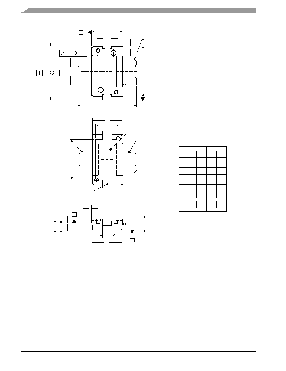
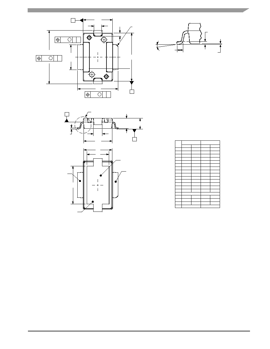
PACKAGE DIMENSIONS
TO-270-2
PLASTIC
CASE 1265-08
ISSUE G
DATUM
PLANE
BOTTOM VIEW
A1
2X
E
D1
E4
E1
D2
E3
A2
EXPOSED
HEATSINK AREA
A
B
D
H
PIN ONE ID
««««
««««
««««
««««
««««
««««
««««
««««
««««
D
A
M
aaa
D
A
M
aaa
D
2X
b1
2X
D3
NOTES:
1. CONTROLLING DIMENSION: INCH.
2. INTERPRET DIMENSIONS AND TOLERANCES
PER ASME Y14.5M-1994.
3. DATUM PLANE -H- IS LOCATED AT TOP OF LEAD
AND IS COINCIDENT WITH THE LEAD WHERE
THE LEAD EXITS THE PLASTIC BODY AT THE
TOP OF THE PARTING LINE.
4. DIMENSIONS
"D1" AND "E1" DO NOT INCLUDE
MOLD PROTRUSION. ALLOWABLE PROTRUSION
IS .006 PER SIDE. DIMENSIONS
"D1" AND "E1" DO
INCLUDE MOLD MISMATCH AND ARE DETER-
MINED AT DATUM PLANE -H-.
5. DIMENSION b1 DOES NOT INCLUDE DAMBAR
PROTRUSION. ALLOWABLE DAMBAR
PROTRUSION SHALL BE .005 TOTAL IN EXCESS
OF THE b1 DIMENSION AT MAXIMUM MATERIAL
CONDITION.
6. DATUMS -A- AND -B- TO BE DETERMINED AT
DATUM PLANE -H-.
7. DIMENSION A2 APPLIES WITHIN ZONE
"J" ONLY.
8. DIMENSIONS
"D" AND "E2" DO NOT INCLUDE
MOLD PROTRUSION. ALLOWABLE PROTRUSION
IS .003 PER SIDE. DIMENSIONS
"D" AND "E2" DO
INCLUDE MOLD MISMATCH AND ARE DETER-
MINED AT DATUM PLANE -D-.
NOTE 7
c1
F
ZONE J
E2
2X
A
DIM
A
MIN
MAX
MIN
MAX
MILLIMETERS
.078
.082
1.98
2.08
INCHES
A1
.039
.043
0.99
1.09
A2
.040
.042
1.02
1.07
D
.416
.424
10.57
10.77
D1
.378
.382
9.60
9.70
D2
.290
.320
7.37
8.13
D3
.016
.024
0.41
0.61
E
.436
.444
11.07
11.28
E1
.238
.242
6.04
6.15
E2
.066
.074
1.68
1.88
E3
.150
.180
3.81
4.57
E4
.058
.066
1.47
1.68
F
b1
.193
.199
4.90
5.06
c1
.007
.011
0.18
0.28
aaa
.025 BSC
.004
0.64 BSC
0.10
PIN 1
PIN 2
PIN 3
STYLE 1:
PIN 1. DRAIN
2. GATE
3. SOURCE
E5
E5
E5
.231
.235
5.87
5.97
MW6S010NR1(MR1)
MW6S010NR1 MW6S010GNR1 MW6S010MR1 MW6S010GMR1
15
RF Device Data
Freescale Semiconductor
TO-270-2 GULL
PLASTIC
CASE 1265A-02
ISSUE A
BOTTOM VIEW
2X
E
D1
E4
E1
D2
E3
A2
EXPOSED
HEATSINK AREA
A
B
D
H
PIN ONE ID
«««««
«««««
«««««
«««««
«««««
«««««
«««««
«««««
«««««
D
A
M
aaa
C
A
M
aaa
C
2X
b1
2X
D3
NOTES:
1. CONTROLLING DIMENSION: INCH.
2. INTERPRET DIMENSIONS AND TOLERANCES
PER ASME Y14.5M-1994.
3. DATUM PLANE -H- IS LOCATED AT TOP OF LEAD
AND IS COINCIDENT WITH THE LEAD WHERE
THE LEAD EXITS THE PLASTIC BODY AT THE
TOP OF THE PARTING LINE.
4. DIMENSIONS
"D1" AND "E1" DO NOT INCLUDE
MOLD PROTRUSION. ALLOWABLE PROTRUSION
IS .006 PER SIDE. DIMENSIONS
"D1" AND "E1" DO
INCLUDE MOLD MISMATCH AND ARE DETER-
MINED AT DATUM PLANE -H-.
5. DIMENSION b1 DOES NOT INCLUDE DAMBAR
PROTRUSION. ALLOWABLE DAMBAR
PROTRUSION SHALL BE .005 TOTAL IN EXCESS
OF THE b1 DIMENSION AT MAXIMUM MATERIAL
CONDITION.
6. DATUMS -A- AND -B- TO BE DETERMINED AT
DATUM PLANE -H-.
7. DIMENSIONS
"D" AND "E2" DO NOT INCLUDE
MOLD PROTRUSION. ALLOWABLE PROTRUSION
IS .003 PER SIDE. DIMENSIONS
"D" AND "E2" DO
INCLUDE MOLD MISMATCH AND ARE DETER-
MINED AT DATUM PLANE -D-.
c1
E2
2X
A
DIM
A
MIN
MAX
MIN
MAX
MILLIMETERS
.078
.082
1.98
2.08
INCHES
A1
.001
.004
0.02
0.10
A2
.077
.088
1.96
2.24
D
.416
.424
10.57
10.77
D1
.378
.382
9.60
9.70
D2
.290
.320
7.37
8.13
D3
.016
.024
0.41
0.61
E
.316
.324
8.03
8.23
E1
.238
.242
6.04
6.15
E2
.066
.074
1.68
1.88
E3
.150
.180
3.81
4.57
E4
.058
.066
1.47
1.68
L1
b1
.193
.199
4.90
5.06
c1
.007
.011
0.18
0.28
aaa
.01 BSC
.004
0.25 BSC
0.10
PIN 1
PIN 2
PIN 3
STYLE 1:
PIN 1. DRAIN
2. GATE
3. SOURCE
e
2
8
2
8
L
.018
.024
4.90
5.06
∞
∞
∞
∞
DETAIL Y
SEATING
PLANE
B
M
bbb
C
L1
L
A1
GAGE
PLANE
e
DETAIL Y
E5
E5
E5
.231
.235
5.87
5.97
MW6S010GNR1(GMR1)

16
RF Device Data
Freescale Semiconductor
MW6S010NR1 MW6S010GNR1 MW6S010MR1 MW6S010GMR1
Information in this document is provided solely to enable system and software
implementers to use Freescale Semiconductor products. There are no express or
implied copyright licenses granted hereunder to design or fabricate any integrated
circuits or integrated circuits based on the information in this document.
Freescale Semiconductor reserves the right to make changes without further notice to
any products herein. Freescale Semiconductor makes no warranty, representation or
guarantee regarding the suitability of its products for any particular purpose, nor does
Freescale Semiconductor assume any liability arising out of the application or use of
any product or circuit, and specifically disclaims any and all liability, including without
limitation consequential or incidental damages. "Typical" parameters that may be
provided in Freescale Semiconductor data sheets and/or specifications can and do
vary in different applications and actual performance may vary over time. All operating
parameters, including "Typicals", must be validated for each customer application by
customer's technical experts. Freescale Semiconductor does not convey any license
under its patent rights nor the rights of others. Freescale Semiconductor products are
not designed, intended, or authorized for use as components in systems intended for
surgical implant into the body, or other applications intended to support or sustain life,
or for any other application in which the failure of the Freescale Semiconductor product
could create a situation where personal injury or death may occur. Should Buyer
purchase or use Freescale Semiconductor products for any such unintended or
unauthorized application, Buyer shall indemnify and hold Freescale Semiconductor
and its officers, employees, subsidiaries, affiliates, and distributors harmless against all
claims, costs, damages, and expenses, and reasonable attorney fees arising out of,
directly or indirectly, any claim of personal injury or death associated with such
unintended or unauthorized use, even if such claim alleges that Freescale
Semiconductor was negligent regarding the design or manufacture of the part.
Freescalet and the Freescale logo are trademarks of Freescale Semiconductor, Inc.
All other product or service names are the property of their respective owners.
Freescale Semiconductor, Inc. 2005. All rights reserved.
How to Reach Us:
Home Page:
www.freescale.com
E-mail:
support@freescale.com
USA/Europe or Locations Not Listed:
Freescale Semiconductor
Technical Information Center, CH370
1300 N. Alma School Road
Chandler, Arizona 85224
+1-800-521-6274 or +1-480-768-2130
support@freescale.com
Europe, Middle East, and Africa:
Freescale Halbleiter Deutschland GmbH
Technical Information Center
Schatzbogen 7
81829 Muenchen, Germany
+44 1296 380 456 (English)
+46 8 52200080 (English)
+49 89 92103 559 (German)
+33 1 69 35 48 48 (French)
support@freescale.com
Japan:
Freescale Semiconductor Japan Ltd.
Headquarters
ARCO Tower 15F
1-8-1, Shimo-Meguro, Meguro-ku,
Tokyo 153-0064
Japan
0120 191014 or +81 3 5437 9125
support.japan@freescale.com
Asia/Pacific:
Freescale Semiconductor Hong Kong Ltd.
Technical Information Center
2 Dai King Street
Tai Po Industrial Estate
Tai Po, N.T., Hong Kong
+800 2666 8080
support.asia@freescale.com
For Literature Requests Only:
Freescale Semiconductor Literature Distribution Center
P.O. Box 5405
Denver, Colorado 80217
1-800-441-2447 or 303-675-2140
Fax: 303-675-2150
LDCForFreescaleSemiconductor@hibbertgroup.com
Document Number: MW6S010
Rev. 1, 5/2005