
This document describes part-number-specific changes to recommended operating conditions
and revised electrical specifications, as applicable, from those described in the general
MPC7455 RISC Microprocessor Hardware Specifications (Order No. MPC7455EC). The
MPC7455 is a PowerPCTM microprocessor.
Specifications provided in this document supersede those in the MPC7455 RISC
Microprocessor Hardware Specifications, Rev. 0 or later, for the part numbers listed in
Table A only. Specifications not addressed herein are unchanged. Because this document is
frequently updated, refer to http://www.motorola.com/semiconductors or to your Motorola
sales office for the latest version.
Note that headings and table numbers in this document are not consecutively numbered. They
are intended to correspond to the heading or table affected in the general hardware
specification.
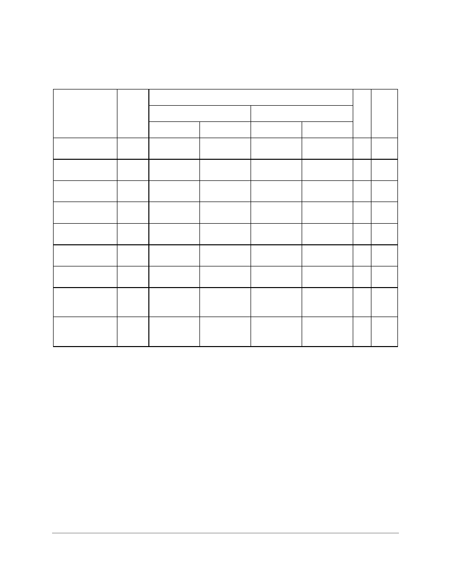
Part numbers addressed in this document are listed in Table A.
Table A. Part Numbers Addressed by this Data Sheet
Motorola
Part Number
Operating Conditions
Significant Differences from
Hardware Specification
CPU
Frequency
(MHz)
V
DD
T
j
(∞C)
XPC7455RX600NC
600
1.3 V ± 50 mV 0 to 105 Modified core and VCO frequency,
and power consumption specifications
XPC7455RX733NC
733
XPC7455RX800NC
800
XPC7445RX600NC
600
XPC7445RX733NC
733
XPC7445RX800NC
800
Note: The X prefix in a Motorola part number designates a "Pilot Production Prototype" as defined by
Motorola SOP 3-13. These are from a limited production volume of prototypes manufactured, tested,
and Q.A. inspected on a qualified technology to simulate normal production. These parts have only
preliminary reliability and characterization data. Before pilot production prototypes may be shipped,
written authorization from the customer must be on file in the applicable sales office acknowledging the
qualification status and the fact that product changes may still occur while shipping pilot production
prototypes.
Advance Information
MPC7455RXNXPNS
Rev. 1.1, 1/2004
MPC7455 Part Number
Specification for the
XPC74x5RXnnnNx Series
Motorola Part
Numbers Affected:
XPC7455RX600NC
XPC7455RX733NC
XPC7455RX800NC
XPC7445RX600NC
XPC7445RX733NC
XPC7445RX800NC
F
r
e
e
s
c
a
l
e
S
e
m
i
c
o
n
d
u
c
t
o
r
,
I
Freescale Semiconductor, Inc.
For More Information On This Product,
Go to: www.freescale.com
n
c
.
.
.
2
MPC7455 Part Number Specification for the XPC74x5RXnnnNx Series
MOTOROLA
Features
Features
1.1
Features
This section summarizes changes to the features of the MPC7455 described in the MPC7455 RISC
Microprocessor Hardware Specifications.
∑
Power management
-- 1.3-V processor core
1.3 General Parameters
∑
Core power supply: 1.3 V ± 50 mV DC nominal
1.5.1 DC Electrical Characteristics
Table 4 provides the recommended operating conditions for the MPC7455 part numbers described herein.
Table 4. Recommended Operating Conditions
Characteristic
Symbol
Recommended
Value
Unit
Core supply voltage
V
DD
1.3 V ± 50 mV
V
PLL supply voltage
AV
DD
1.3 V ± 50 mV
V
Note: These are the recommended and tested operating conditions. Proper device operation outside of these
conditions is not guaranteed.
F
r
e
e
s
c
a
l
e
S
e
m
i
c
o
n
d
u
c
t
o
r
,
I
Freescale Semiconductor, Inc.
For More Information On This Product,
Go to: www.freescale.com
n
c
.
.
.
MOTOROLA
MPC7455 Part Number Specification for the XPC74x5RXnnnNx Series
3
General Parameters
Table 7 provides the power consumption for the MPC7455 part numbers described herein.
Table 7. Power Consumption for MPC7455
Processor (CPU) Frequency
Unit
Notes
600 MHz
733 MHz
800 MHz
Full-Power Mode
Typical 8.4
10.3
11.2
W
1,
3
Maximum 11.9
14.5
15.9
W
1,
2
Doze Mode
Typical --
--
--
W
1,
2,
4
Nap Mode
Typical
1.4
1.7
1.8
W
1, 2
Sleep Mode
Typical
700
800
900
mW
1, 2
Deep Sleep Mode (PLL Disabled)
Typical
470
490
500
mW
1, 3
Notes:
1. These values apply for all valid processor bus and L3 bus ratios. The values do not include I/O supply power (OV
DD
and GV
DD
) or PLL supply power (AV
DD
). OV
DD
and GV
DD
power is system dependent, but is typically < 5% of V
DD
power. Worst case power consumption for AV
DD
< 3 mW.
2. Maximum power is measured at nominal V
DD
while running an entirely cache-resident, contrived sequence of
instructions which keep the execution units, with or without AltiVec, maximally busy.
3. Typical power is an average value measured at nominal V
DD
in a system while running a typical code sequence.
4. Doze mode is not a user-definable state; it is an intermediate state between full-power and either nap or sleep mode.
As a result, power consumption for this mode is not tested.
F
r
e
e
s
c
a
l
e
S
e
m
i
c
o
n
d
u
c
t
o
r
,
I
Freescale Semiconductor, Inc.
For More Information On This Product,
Go to: www.freescale.com
n
c
.
.
.
4
MPC7455 Part Number Specification for the XPC74x5RXnnnNx Series
MOTOROLA
General Parameters
General Parameters
Table 8 provides the clock AC timing specifications for the MPC7455 part numbers described herein.
Table 12 provides the L3 bus interface AC timing specifications for MSUG2 for the MPC7455 part numbers
described herein.
Table 8. Clock AC Timing Specifications
At recommended operating conditions. See Table 4.
Characteristic
Symbol
Maximum Processor Core Frequency
Unit
Notes
600 MHz
733 MHz
800 MHz
Min
Max
Min
Max
Min
Max
Processor frequency
f
core
500
600
500
733
500
800
MHz
1
VCO frequency
f
VCO
1000
1200
1000
1466
1000
1600
MHz
1
Notes:
1. Caution: The SYSCLK frequency, PLL_CFG[0:4] settings must be chosen such that the resulting SYSCLK (bus)
frequency, CPU (core) frequency, and PLL (VCO) frequency do not exceed their respective maximum or minimum
operating frequencies (see Table 4 in the MPC7455 RISC Microprocessor Hardware Specifications). Refer to the
PLL_CFG[0:4] signal description in Section 1.9.1, "PLL Configuration," for valid PLL_CFG[0:4] settings.
Table 12. L3 Bus Interface AC Timing Specifications for MSUG2
At recommended operating conditions. See Table 4.
Parameter
Symbol
All Speed Grades
Unit
Notes
L2CR[12] = 0 and L3CR[12] = 0
8
L2CR[12] = 1 and L3CR[12] = 1
8
Min
Max
Min
Max
L3_CLK rise and
fall time
t
L3CR
,
t
L3CF
--
1.0
--
1.0
ns
1
Setup times:
Data and parity
t
L3DVEH
,
t
L3DVEL
≠0.1
--
≠0.1
--
ns
2, 3, 4
Input hold times:
Data and parity
t
L3DXEH
,
t
L3DXEL
t
L3_ECHO_CLK
/4
+ 0.6
--
t
L3_ECHO_CLK
/4
+0.6
--
ns
2, 4
Valid times:
Data and parity
t
L3CHDV
,
t
L3CLDV
--
(≠ t
L3_CLK
/4)
+ 0.4
--
(≠ t
L3_CLK
/4)
+ 0.8
ns
5, 6, 7
Valid times:
All other outputs
t
L3CHOV
--
t
L3_CLK
/4 + 1.0
--
t
L3_CLK
/4 + 1.2
ns
5, 7
Output hold times:
Data and parity
t
L3CHDX
,
t
L3CLDX,
t
L3_CLK
/4 ≠ 0.4
--
t
L3_CLK
/4 ≠ 0.2
--
ns
5, 6, 7
Output hold times:
All other outputs
t
L3CHOX
t
L3_CLK
/4 ≠ 0.5
--
t
L3_CLK
/4 ≠ 0.3
--
ns
5, 7
L3_CLK to high
impedance:
Data and parity
t
L3CLDZ
--
t
L3_CLK
/2
--
t
L3_CLK
/2
ns
F
r
e
e
s
c
a
l
e
S
e
m
i
c
o
n
d
u
c
t
o
r
,
I
Freescale Semiconductor, Inc.
For More Information On This Product,
Go to: www.freescale.com
n
c
.
.
.
MOTOROLA
MPC7455 Part Number Specification for the XPC74x5RXnnnNx Series
5
General Parameters
L3_CLK to high
impedance:
All other outputs
t
L3CHOZ
--
t
L3_CLK
/4 + 2.0
--
t
L3_CLK
/4 + 2.0
ns
Notes:
1. Rise and fall times for the L3_CLK output are measured from 20% to 80% of GV
DD
.
2. For DDR, all input specifications are measured from the midpoint of the signal in question to the midpoint voltage
of the rising or falling edge of the input L3_ECHO_CLKn (see Figure 10 in the MPC7455 RISC Microprocessor
Hardware Specifications). Input timings are measured at the pins.
3. For DDR, the input data will typically follow the edge of L3_ECHO_CLKn as shown in Figure 10 in the MPC7455
RISC Microprocessor Hardware Specifications. For consistency with other input setup time specifications, this will
be treated as negative input setup time.
4. t
L3_ECHO_CLK
/4 is one-fourth the period of L3_ECHO_CLKn. This parameter indicates that the MPC7455 can latch
an input signal that is valid for only a short time before and a short time after the midpoint between the rising and
falling (or falling and rising) edges of L3_ECHO_CLKn at any frequency.
5. All output specifications are measured from the midpoint voltage of the rising (or for DDR write data, also the falling)
edge of L3_CLK to the midpoint of the signal in question. The output timings are measured at the pins. All output
timings assume a purely resistive 50-
load (see Figure 8 in the MPC7455 RISC Microprocessor Hardware
Specifications).
6. For DDR, the output data will typically lead the edge of L3_CLKn as shown in Figure 10 in the MPC7455 RISC
Microprocessor Hardware Specifications. For consistency with other output valid time specifications, this will be
treated as negative output valid time.
7. t
L3_CLK
/4 is one-fourth the period of L3_CLKn. This parameter indicates that the specified output signal is actually
launched by an internal clock delayed in phase by 90∞. Therefore, there is a frequency component to the output valid
and output hold times such that the specified output signal will be valid for approximately one L3_CLK period
starting three-fourths of a clock prior to the edge on which the SRAM will sample it and ending one-fourth of a clock
period after the edge it will be sampled.
8. These configuration bits allow the AC timing of the L3 interface to be altered via software. They must be both set or
both cleared; other configurations will increase t
L3CSKW1
, which may cause unreliable L3 operation.
Table 12. L3 Bus Interface AC Timing Specifications for MSUG2 (continued)
At recommended operating conditions. See Table 4.
Parameter
Symbol
All Speed Grades
Unit
Notes
L2CR[12] = 0 and L3CR[12] = 0
8
L2CR[12] = 1 and L3CR[12] = 1
8
Min
Max
Min
Max
F
r
e
e
s
c
a
l
e
S
e
m
i
c
o
n
d
u
c
t
o
r
,
I
Freescale Semiconductor, Inc.
For More Information On This Product,
Go to: www.freescale.com
n
c
.
.
.
6
MPC7455 Part Number Specification for the XPC74x5RXnnnNx Series
MOTOROLA
General Parameters
General Parameters
Table 13 provides the L3 bus AC timing specifications for PB2 and Late Write SRAMs for the MPC7455
part numbers described herein.
Table 13. L3 Bus Interface AC Timing Specifications for PB2 and Late Write SRAMs
At recommended operating conditions. See Table 4.
Parameter
Symbol
All Speed Grades
Unit
Notes
L2CR[12]=0 and L3CR[12]=0
6
L2CR[12]=1 and L3CR[12]=1
6
Min
Max
Min
Max
L3_CLK rise and fall
time
t
L3CR
,
t
L3CF
--
1.0
--
1.0
ns
1, 5
Setup times:
Data and parity
t
L3DVEH
1.5
--
1.5
--
ns
2, 5
Input hold times:
Data and parity
t
L3DXEH
--
0.5
--
0.5
ns
2, 5
Valid times:
Data and parity
t
L3CHDV
--
t
L3_CLK
/4 + 1.0
--
t
L3_CLK
/4 + 1.2
ns
3, 4, 5
Valid times:
All other outputs
t
L3CHOV
--
t
L3_CLK
/4 + 1.0
--
t
L3_CLK
/4 + 1.2
ns
4
Output hold times:
Data and parity
t
L3CHDX
t
L3_CLK
/4 ≠ 0.4
--
t
L3_CLK
/4 ≠ 0.2
--
ns
3, 4, 5
Output hold times:
All other outputs
t
L3CHOX
t
L3_CLK
/4 ≠ 0.4
--
t
L3_CLK
/4 ≠ 0.2
--
ns
4, 5
L3_CLK to high
impedance:
Data and parity
t
L3CHDZ
--
2.0
--
2.0
ns
5
L3_CLK to high
impedance:
All other outputs
t
L3CHOZ
--
2.0
--
2.0
ns
5
Notes:
1. Rise and fall times for the L3_CLK output are measured from 20% to 80% of GV
DD
.
2. All input specifications are measured from the midpoint of the signal in question to the midpoint voltage of the rising
edge of the input L3_ECHO_CLKn (see Figure 10 in the MPC7455 RISC Microprocessor Hardware Specifications).
Input timings are measured at the pins.
3. All output specifications are measured from the midpoint voltage of the rising edge of L3_CLKn to the midpoint of
the signal in question. The output timings are measured at the pins. All output timings assume a purely resistive
50-
load (see Figure 10 in the MPC7455 RISC Microprocessor Hardware Specifications).
4. t
L3_CLK
/4 is one-fourth the period of L3_CLKn. This parameter indicates that the specified output signal is actually
launched by an internal clock delayed in phase by 90∞. Therefore, there is a frequency component to the output valid
and output hold times such that the specified output signal will be valid for approximately one L3_CLK period
starting three-fourths of a clock prior to the edge on which the SRAM will sample it and ending one-fourth of a clock
period after the edge it will be sampled.
5. Timing behavior and characterization are currently being evaluated.
6. These configuration bits allow the AC timing of the L3 interface to be altered via software. They must be both set or
both cleared; other configurations will increase t
L3CSKW1
and t
L3CSKW2
, which may cause unreliable L3 operation.
F
r
e
e
s
c
a
l
e
S
e
m
i
c
o
n
d
u
c
t
o
r
,
I
Freescale Semiconductor, Inc.
For More Information On This Product,
Go to: www.freescale.com
n
c
.
.
.
MOTOROLA
MPC7455 Part Number Specification for the XPC74x5RXnnnNx Series
7
General Parameters
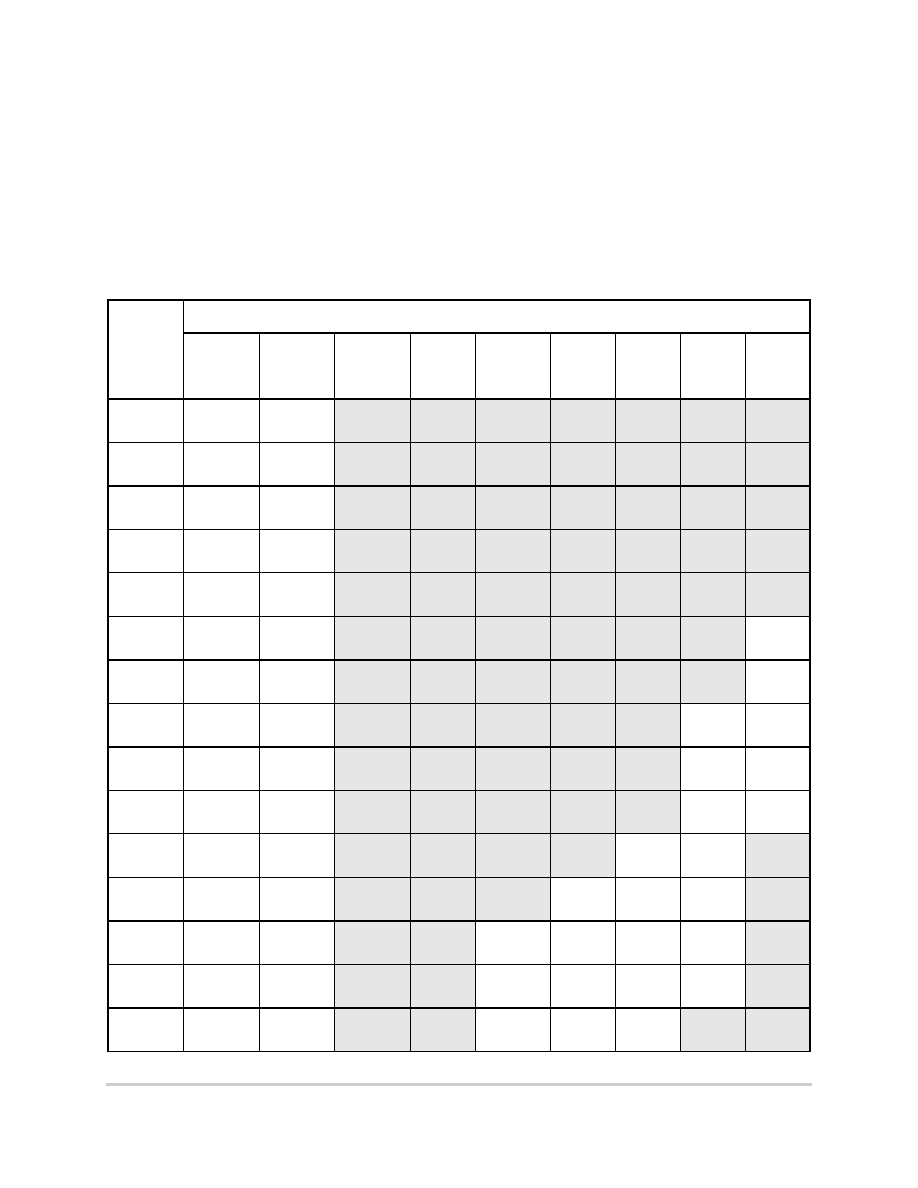
1.9.1 PLL Configuration
The MPC7455 PLL is configured by the PLL_CFG[0:4] signals; note that PLL_CFG[4] was formerly called
PLL_EXT in earlier documentation. For a given SYSCLK (bus) frequency, the PLL configuration signals
set the internal CPU and VCO frequency of operation. PLL_CFG[4] will normally be pulled low but can be
asserted for extended modes of operation. The PLL configuration for the MPC7455 is shown in Table 17
for a set of example frequencies. In this example, shaded cells represent settings that, for a given SYSCLK
frequency, result in core and/or VCO frequencies that do not comply with the 1-GHz column in Table 8.
Note that the settings for Rev. C devices are different than those for subsequent devices.
Table 17. MPC7455 Microprocessor PLL Configuration Example for 800-MHz Parts
PLL_CFG
[0:4]
Example Bus-to-Core Frequency in MHz (VCO Frequency in MHz)
Bus-to-
Core
Multiplier
Core-to-
VCO
Multiplier
Bus
33.3 MHz
Bus
50 MHz
Bus
66.6 MHz
Bus
75 MHz
Bus
83 MHz
Bus
100 MHz
Bus
133 MHz
00000
0.5x
2x
01000
2x
2x
01100
2.5x
2x
10000
3x
2x
11100
3.5x
2x
10100
4x
2x
533
(1066)
01110
4.5x
2x
600
(1200)
10110
5x
2x
500
(1000)
667
(1333)
10010
5.5x
2x
550
(1100)
733
(1466)
11010
6x
2x
600
(1200)
800
(1600)
01010
6.5x
2x
540
(1080)
650
(1300)
00100
7x
2x
525
(1050)
580
(1160)
700
(1400)
00010
7.5x
2x
500
(1000)
563
(1125)
623
(1245)
750
(1500)
11000
8x
2x
533
(1066)
600
(1200)
664
(1328)
800
(1600)
01111
9x
2x
600
(1200)
675
(1350)
747
(1494)
F
r
e
e
s
c
a
l
e
S
e
m
i
c
o
n
d
u
c
t
o
r
,
I
Freescale Semiconductor, Inc.
For More Information On This Product,
Go to: www.freescale.com
n
c
.
.
.
8
MPC7455 Part Number Specification for the XPC74x5RXnnnNx Series
MOTOROLA
General Parameters
General Parameters
10101
10x
2x
500
(1000)
667
(1333)
750
(1500)
10011
11x
2x
550
(1100)
733
(1466)
10111
12x
2x
600
(1200)
800
(1600)
01011
13x
2x
650
(1300)
11001
14x
2x
700
(1400)
00011
15x
2x
500
(1000)
750
(1500)
11011
16x
2x
533
(1066)
800
(1600)
00110
PLL off/bypass
PLL off, SYSCLK clocks core circuitry directly
11110
PLL off
PLL off, no core clocking occurs
Table 17. MPC7455 Microprocessor PLL Configuration Example for 800-MHz Parts (continued)
PLL_CFG
[0:4]
Example Bus-to-Core Frequency in MHz (VCO Frequency in MHz)
Bus-to-
Core
Multiplier
Core-to-
VCO
Multiplier
Bus
33.3 MHz
Bus
50 MHz
Bus
66.6 MHz
Bus
75 MHz
Bus
83 MHz
Bus
100 MHz
Bus
133 MHz
F
r
e
e
s
c
a
l
e
S
e
m
i
c
o
n
d
u
c
t
o
r
,
I
Freescale Semiconductor, Inc.
For More Information On This Product,
Go to: www.freescale.com
n
c
.
.
.
MOTOROLA
MPC7455 Part Number Specification for the XPC74x5RXnnnNx Series
9
Ordering Information
1.11 Ordering Information
1.11.1 Part Numbers Addressed by this Specification
Table 21 provides the ordering information for the MPC7455 parts described in this document.
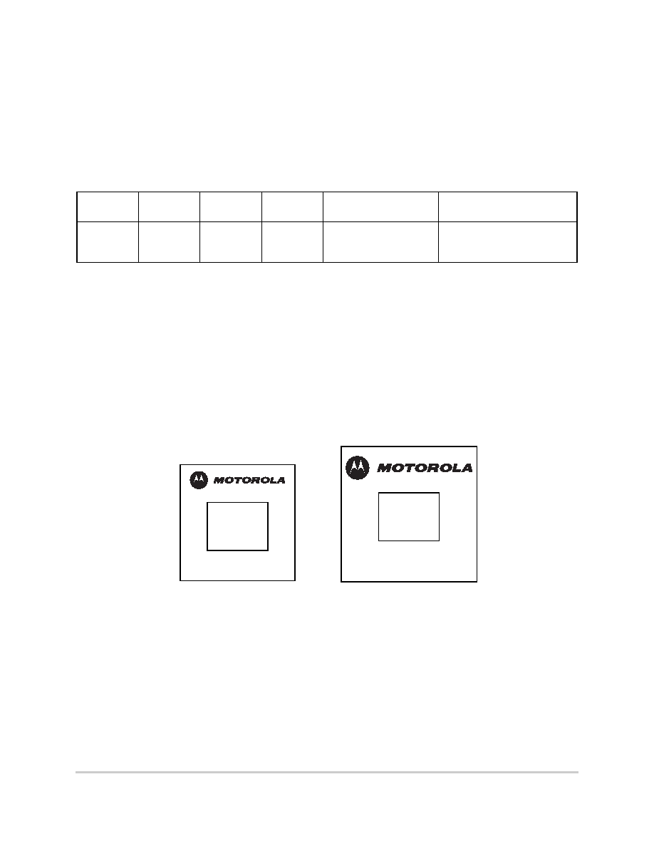
1.11.3 Part Marking
Parts are marked as the example shown in Figure 29.
Figure 29. Motorola Part Marking for BGA Devices
Table 21. Part Marking Nomenclature
XPC
74x5
RX
nnn
x
x
Product
Code
Part
Identifier
Package
Processor
Frequency
1
1
Processor core frequencies supported by parts addressed by this specification only. Parts addressed by other
specifications may support other maximum core frequencies.
Application Modifier
Revision Level
XPC
2
2
The X prefix in a Motorola part number designates a "Pilot Production Prototype" as defined by Motorola SOP 3-13.
These are from a limited production volume of prototypes manufactured, tested, and Q.A. inspected on a qualified
technology to simulate normal production. These parts have only preliminary reliability and characterization data.
Before pilot production prototypes may be shipped, written authorization from the customer must be on file in the
applicable sales office acknowledging the qualification status and the fact that product changes may still occur while
shipping pilot production prototypes.
7455
7445
RX = CBGA
600
733
800
N: 1.3 V ± 50 mV
0 to 105
∞
C
C: 2.1; PVR = 8001 0201
Notes:
BGA
Notes
:
CCCCC is the country of assembly. This space is left blank if parts are assembled in the United States.
MMMMMM is the 6-digit mask number.
ATWLYYWWA is the traceability code.
XPC7455
RX800NC
MMMMMM
ATWLYYWWA
7450
BGA
XPC7445
RX8000NC
MMMMMM
ATWLYYWWA
7440
F
r
e
e
s
c
a
l
e
S
e
m
i
c
o
n
d
u
c
t
o
r
,
I
Freescale Semiconductor, Inc.
For More Information On This Product,
Go to: www.freescale.com
n
c
.
.
.
10
MPC7455 Part Number Specification for the XPC74x5RXnnnNx Series
MOTOROLA
Document Revision History
Document Revision History
Document Revision History
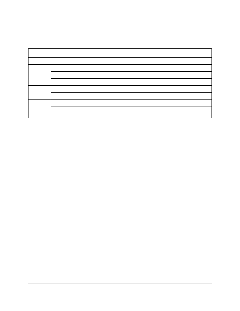
Table B provides a revision history for this part number specification.
Table B. Document Revision History
Rev. No.
Substantive Change(s)
0
Initial release.
0.1
Updated wording in Table A, `Significant Differences from Hardware Specification,' column.
Corrected part number in heading of Table 7 (changed from MPC7450 to MPC7455).
Added Document Revision History section and Table B.
1
Updated Table 7, note 1.
Added Tables 2, 12, 13, and 17.
1.1
Tabled 9: corrected typo in units for Sleep Mode power, changed "W" to "mW".
Table 17: corrected PLL_CFG values; previous revisions of this specification had swapped PLL_CFG[0]
with PLL_CFG[4].
F
r
e
e
s
c
a
l
e
S
e
m
i
c
o
n
d
u
c
t
o
r
,
I
Freescale Semiconductor, Inc.
For More Information On This Product,
Go to: www.freescale.com
n
c
.
.
.

MOTOROLA
MPC7455 Part Number Specification for the XPC74x5RXnnnNx Series
11
Document Revision History
THIS PAGE INTENTIONALLY LEFT BLANK
F
r
e
e
s
c
a
l
e
S
e
m
i
c
o
n
d
u
c
t
o
r
,
I
Freescale Semiconductor, Inc.
For More Information On This Product,
Go to: www.freescale.com
n
c
.
.
.

MPC7455RXNXPNS
HOW TO REACH US:
USA/EUROPE/LOCATIONS NOT LISTED:
Motorola Literature Distribution
P.O. Box 5405, Denver, Colorado 80217
1-480-768-2130
(800) 521-6274
JAPAN:
Motorola Japan Ltd.
SPS, Technical Information Center
3-20-1, Minami-Azabu Minato-ku
Tokyo 106-8573 Japan
81-3-3440-3569
ASIA/PACIFIC:
Motorola Semiconductors H.K. Ltd.
Silicon Harbour Centre, 2 Dai King Street
Tai Po Industrial Estate, Tai Po, N.T., Hong Kong
852-26668334
TECHNICAL INFORMATION CENTER:
(800) 521-6274
HOME PAGE:
www.motorola.com/semiconductors
Information in this document is provided solely to enable system and software implementers to use
Motorola products. There are no express or implied copyright licenses granted hereunder to design
or fabricate any integrated circuits or integrated circuits based on the information in this document.
Motorola reserves the right to make changes without further notice to any products herein.
Motorola makes no warranty, representation or guarantee regarding the suitability of its products
for any particular purpose, nor does Motorola assume any liability arising out of the application or
use of any product or circuit, and specifically disclaims any and all liability, including without
limitation consequential or incidental damages. "Typical" parameters which may be provided in
Motorola data sheets and/or specifications can and do vary in different applications and actual
performance may vary over time. All operating parameters, including "Typicals" must be validated
for each customer application by customer's technical experts. Motorola does not convey any
license under its patent rights nor the rights of others. Motorola products are not designed,
intended, or authorized for use as components in systems intended for surgical implant into the
body, or other applications intended to support or sustain life, or for any other application in which
the failure of the Motorola product could create a situation where personal injury or death may
occur. Should Buyer purchase or use Motorola products for any such unintended or unauthorized
application, Buyer shall indemnify and hold Motorola and its officers, employees, subsidiaries,
affiliates, and distributors harmless against all claims, costs, damages, and expenses, and
reasonable attorney fees arising out of, directly or indirectly, any claim of personal injury or death
associated with such unintended or unauthorized use, even if such claim alleges that Motorola was
negligent regarding the design or manufacture of the part.
Motorola and the Stylized M Logo are registered in the U.S. Patent and Trademark Office.
digital dna is a trademark of Motorola, Inc. The described product is a PowerPC microprocessor.
The PowerPC name is a trademark of IBM Corp. and used under license. All other product or
service names are the property of their respective owners. Motorola, Inc. is an Equal
Opportunity/Affirmative Action Employer.
© Motorola, Inc. 2004
F
r
e
e
s
c
a
l
e
S
e
m
i
c
o
n
d
u
c
t
o
r
,
I
Freescale Semiconductor, Inc.
For More Information On This Product,
Go to: www.freescale.com
n
c
.
.
.