 | –≠–ª–µ–∫—Ç—Ä–æ–Ω–Ω—ã–π –∫–æ–º–ø–æ–Ω–µ–Ω—Ç: 828BR | –°–∫–∞—á–∞—Ç—å:  PDF PDF  ZIP ZIP |
25 Locust St, Haverhill, Massachusetts 01830 ∑ Tel: 800/252-7074, 978/374-0761 ∑ FAX: 978/521-1839
e-mail: sales@freqdev.com ∑ Web Address: http://www.freqdev.com
Applications
∑ Power line interference rejection
∑ Transducer output filtering
∑ Production test instrumentation
∑ Medical electronics equipment and research
∑ Comb filtering and equalization
∑ Noise and harmonic analysis
∑ RMS measurements
∑ Frequency spectrum analysis
Features/Benefits:
∑ Compact 2.0"L x 2.0"W footprint minimizes board
space requirements.
∑ Plug-in ready-to-use, reducing engineering design
and manufacturing cycle time.
∑ Factory tuned, no external clocks or adjustments
needed.
∑ Broad range of center frequencies to meet a wide
range of applications.
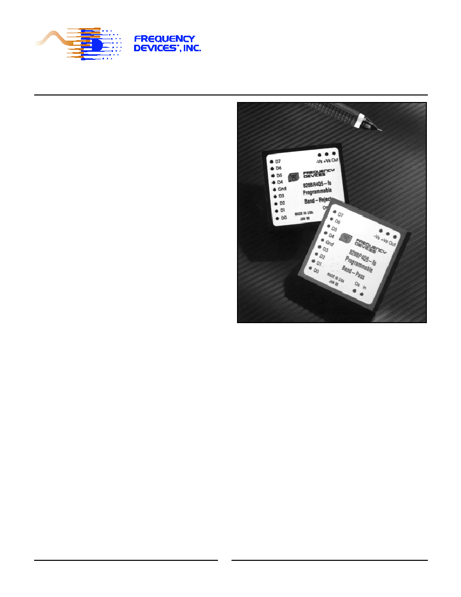
Description:
The 828BP and 828BR Series are 4-pole-pair
digitally programmable band-pass and band-reject
(notch) active filters. These new filters take
advantage of the company's proprietary designs
using surface-mount technology to provide a low
profile, compact package in minimal board space.
828BP and 828BR filters are factory tuned to one of
three factory set tuning ranges or 8-bit custom
ranges from 1 Hz to 25.6 kHz. Each filter type
features a near theoretical amplitude/phase
response along with low output voltage noise
enabling these filters to achieve a 10,000:1 or better
dynamic signal range
Pretuned to within ±2% of the center frequency,
band-pass 828BP filters pass all frequencies lying
between the upper and lower -3 dB points of the
amplitude response curve, while 828BR band-reject
(notch) filters sharply attenuate those frequencies
that are bound and defined by the bottom of the
notch. Available Q's for 828BP models are 1, 2, 5, or
10 and 828BR filters are 3 or 10.
Band Pass and Band Reject
828BP & 828BR Series
8 Bit Programmable
4-Pole Pair Filters
1
Programmable Specifications:
. . . . . . . . . . . .
Page
Digital Tuning & Control . . . . . . . . . . . . . . . . . . . . .2
Available Band-Pass Models:
828BP4
4 pole pair . . . . . . . . . . . . . . . . . . .3
Available Band-Reject Models:
828BR4
4-pole pair . . . . . . . . . . . . . . . . . . .3
General Specifications:
Ordering Information . . . . . . . . . . . . . . . . . . . . . . .4
Pin-Out/package data . . . . . . . . . . . . . . . . . . . . . .4
828BP & 828BR Series
Digital Tuning &
Control Characteristics
25 Locust St, Haverhill, Massachusetts 01830 ∑ Tel: 800/252-7074, 978/374-0761 ∑ FAX: 978/521-1839
e-mail: sales@freqdev.com ∑ Web Address: http://www.freqdev.com
8-Bit Programmable Filters
2
Digital Tuning Characteristics
The digital tuning interface circuits are a parallel set of eight
(8) 4053 CMOS switches which accept CMOS compatible
inputs for the eight tuning bits (D
0
- D
7
).
Filter tuning follows the tuning equation given below:
f
c
= ( f
max
/256 ) [ 1 + D
7
x 2
7
+ D
6
x 2
6
+ D
5
x 2
5
+ D
4
x 2
4
+
D
3
x 2
3
+ D
2
x 2
2
+ D
1
x 2
1
+ D
0
x 2
0
]
where D
1
- D
7
= "0" or "1", and
f
max
= Maximum tuning frequency;
f
c
= corner frequency;
Minimum tunable frequency = f
max
/256 (D
0
thru D
7
= 0);
Minimum frequency step (Resolution) = f
max
/256
Data Input Specifications
Input Data Levels
(CMOS Logic)
Input Voltage (Vs = 15 Vdc)
Low Level In
0 Vdc min.
4 Vdc max.
High Level In
11 Vdc min.
15 Vdc max.
Input Current
High Level In
- 10
-5
µA typ.
-1
µA max.
.
Low Level In
+10
-5
µA typ
.
+1
µA max.
Input Capacitance
5 pF typ
7.5 pF max.
Input Data Format
Frequency Select Bits
Positive Logic
Logic "1" = +Vs
Logic "0" = Gnd
Bit Weighting
(Binary-Coded)
D
0
LSB (least significant bit)
D
7
MSB (most significant bit)
Frequency Range
256 : 1, Binary Weighted
Pin-Out Key
IN
Analog Input Signal
D
7
Tuning Bit 7 (MSB)
OUT Analog Output Signal
D
6
Tuning Bit 6
GND Power and Signal Return
D
5
Tuning Bit 5
+Vs
Supply Voltage, Positive
D
4
Tuning Bit 4
-Vs
Supply Voltage, Negative
D
3
Tuning Bit 3
Os
Offset Adjustment
D
2
Tuning Bit 2
D
1
Tuning Bit 1
D
0
Tuning Bit 0 (LSB)
MSB
---
---
---
---
---
---
LSB
Bit
Weight
2
7
2
6
2
5
2
4
2
3
2
2
2
1
2
0
fc
Corner
Frequency
D
7
D
6
D
5
D
4
D
3
D
2
D
1
D
0
0
0
0
0
0
0
0
0
f
max
/256
0
0
0
0
0
0
0
1
f
max
/128
0
0
0
0
0
0
1
1
f
max
/64
0
0
0
0
0
1
1
1
f
max
/32
0
0
0
0
1
1
1
1
f
max
/16
0
0
0
1
1
1
1
1
f
max
/8
0
0
1
1
1
1
1
1
f
max
/4
0
1
1
1
1
1
1
1
f
max
/2
1
1
1
1
1
1
1
1
fmax
+Vs
OUT
-Vs
D
D
D
D
GND
D
D
D
D
IN
2.00
Bottom View
Os
4
5
3
2
1
0
6
7
4
Band-Pass & Band-Reject
828BP & 828BR Series
8-Bit Programmable
4-Pole Pair Filters
25 Locust St, Haverhill, Massachusetts 01830 ∑ Tel: 800/252-7074, 978/374-0761 ∑ FAX: 978/521-1839
e-mail: sales@freqdev.com ∑ Web Address: http://www.freqdev.com
Model
828BP4
Model
828BR4
Product Specifications
Band-Pass
Product Specifications
Band-Reject
Size
2.0" x 2.0" x 0.5"
Size
2.0" x 2.0" x 0.5"
Range fo
1 Hz to 25.6 kHz
Range fo
1 Hz to 25.6 kHz
Available "Q's"
1
1, 2, 5, 10
Available "Q's"
1
3, 10
Q Accuracy
±10%
Q Accuracy
±10%
Theoretical Transfer
Appendix A
Theoretical Transfer
Appendix A
Characteristics
Pages 41 & 42
Characteristics
Pages 43
Notch Attenuation
45 db typ.
Pass-Band Gain
0± 0.25 dB typ.
Pass-Band Gain
0± 0.25 dB typ.
(non-inverting)
0± 0.50 dB max.
(non-inverting)
0± 0.50 dB max.
Attenuation Rate
24 dB/octave
Attenuation Rate
24 dB/octave
Center Frequency
fo
±2% max.
Center Frequency
fo
±2% max.
Stability
±0.01%/∞C
Stability
±0.01%/∞C
Filter Mounting
FMA-02A
Filter Mounting
FMA-02A
Assembly
Assembly
1. Q ≠ Quality Factor for band-pass and band-reject filters. Q = f
O
/(f
H
-f
L
)
f
O
=
f
H
f
L
3
828BP & 828BR Series
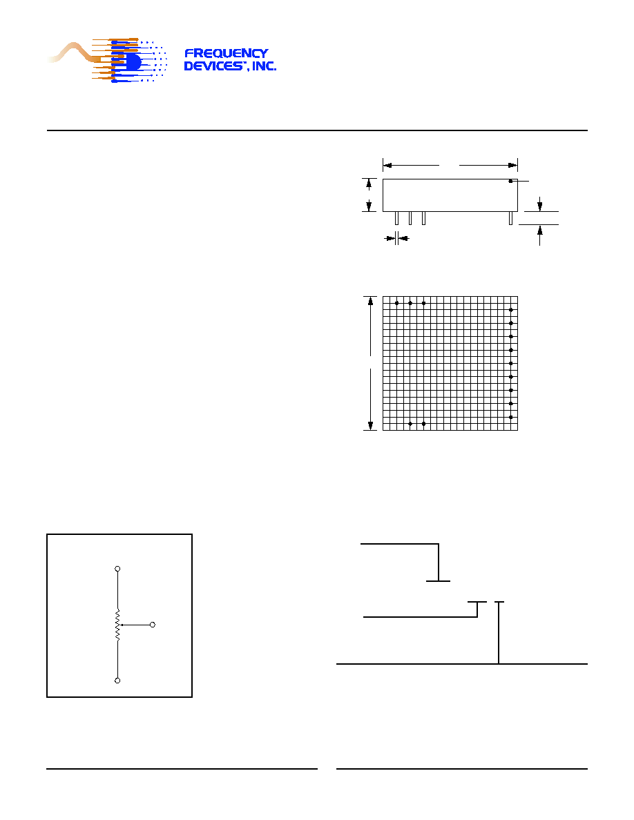
Pin-Out and Package Data
Ordering Information
We hope the information given here will be helpful. The information is based on data and our best knowledge, and we consider the information to be true and accurate. Please read all statements,
recommendations or suggestions herein in conjunction with our conditions of sale which apply to all goods supplied by us. We assume no responsibility for the use of these statements,
recommendations or suggestions, nor do we intend them as a recommendation for any use which would infringe any patent or copyright.
PR-828BP/BR-03
25 Locust St, Haverhill, Massachusetts 01830 ∑ Tel: 800/252-7074, 978/374-0761 ∑ FAX: 978/521-1839
e-mail: sales@freqdev.com ∑ Web Address: http://www.freqdev.com
4
Specification
(25∞C and Vs ±15Vdc)
DC Offset Adjustment
± Vs
- Vs
20 k
(Cermet)
Do not connect
if trim is not
required.
OS
Analog Input Characteristics
1
Impedance
10 k
min.
Voltage Range
±
10 Vpeak
Max. Safe Voltage
±
Vs
Analog Output Characteristics
Impedance (Closed Loop)
1
1
typ.
10
max.
Linear Operating Range
±
10V
Maximum Current
2
±
2 mA
Offset Voltage
3
2
2 mV typ.
20 mV max.
Offset Temp. Coeff.
50
µV/∞C
Power Supply (
±
V)
Rated Voltage
±
15 Vdc
Operating Range
±
12 to
±
18 Vdc
Maximum Safe Voltage
±
18 Vdc
Quiescent Current
±
25 mA typ.
±
40 mA max.
Temperature
Operating
-2
0 to +70∞C
Storage
-25 to +85∞C
Notes:
1. Input and output signal voltage referenced to supply common.
2. Output is short circuit protected to common.
DO NOT CONNECT TO ±Vs.
3. Adjustable to zero.
4. Units operate with or without offset pin connected.
828BP4/10-4
Model
Tuning
Minimum
Number
Range (Hz)
Step(Hz)
Case
2
1.0 to 256
1.0
G-3
3
10 to 2560
10
G-3
4
100 to 25.6k
100
G-3
Model
Filter Type
BP - Band Pass
BR - Band Reject
Ordering Information
Side View
+Vs
OUT
-Vs
D
D
D
D
GND
D
D
D
D
IN
2.00
Bottom View
0.15 min.
0.025 Dia.
Os
4
5
3
2
1
0
6
7
4
G-3
0.5
2.00
All dimensions are in inches
All Case Dimensions ± 0.02"
Grid Dimensions 0.1" x 0.1"
Filter Mounting Assembly-See FMA-02A
Pin-Out & Package Data
"Q"
BP - 1, 2, 5, 10
BR - 3, 10

25 Locust St, Haverhill, Massachusetts 01830 ∑ Tel: 800/252-7074, 978/374-0761 ∑ FAX: 978/521-1839
e-mail: sales@freqdev.com ∑ Web Address: http://www.freqdev.com
November 2000
Programmable Filters Modules
818, 824, 828, 828BP, 828BR, 854, 858, R854, R858
I. Scope
The following precautions are necessary when handling and installing Frequency Devices
programmable filter modules.
II. Digital Circuit Description
The digital input pins connect directly to 4000 series CMOS logic, such as the 4053 analog switch. The
power supply (Vss) for the digital logic on the module comes directly from the +15 Volt pin on the
module. This sets the threshold voltage at 11.0 V minimum to 15.0 V maximum for a "1" (High) level
and 0.0 V minimum to 4.0 V maximum for a "0" (Low) level. Applying a voltage between 4.0 and 11.0
V will produce unpredictable operation. Connecting 5 Volt or 3.3 V logic devices directly to the filter
module without using a voltage translator will result in erratic operation of the filter.
III. (VERY IMPORTANT) Power-Up and Power-Down Sequence
Do not plug-in or un-plug module while power is applied.
It is imperative that power is
supplied to the + 15 V pin on the filter module before or at the same instance that any digital pin is
pulled High (> 0.0 V). Failure to do this will result in excessive current flowing through the digital input
pin and through a protection diode internal to the 4000 logic, which will result in damage to the module.
The proper power-up and power-down sequence is:
1. Connect filter module ground.
2. Connect filter module +15 V.
3. Connect filter module -15 V.
4. Connect the input signal.
All four of the above steps can also occur simultaneously. Power-down should occur in the reverse
order.
IV. ESD Issues
Like most modern electronic equipment, the modules can be damaged by electrostatic discharge (ESD).
The modules are shipped from the factory in sealed, anti-static packaging and should be kept in the
sealed package prior to mounting on a circuit board. The following additional rules should also be
observed when handling the modules after they are removed from the factory packaging:
1. Only a person wearing a properly grounded wrist strap should handle the modules.
2. Any work surface that the modules are placed on must be properly ESD grounded.
3. Any insulating materials capable of generating static charge (such as paper) should be kept
away from the modules.
Static generating clothing should be covered with an ESD-protective smock.
1
Product Handling
Procedure
Programmable Filter Modules Power Sequence & ESD