FREQUENCY MANAGEMENT | INTERNATIONAL
15302 Bolsa Chica Street
Huntington Beach, CA 92649
ph (714) 373-8100 | fx (714) 373-8700
1-800-800-XTAL
[9825]
www.fmi-inc.com
NOTE: Waveforms & Test Circuits on pages 48, 49
Standard Specifications for product indicated in
color
38
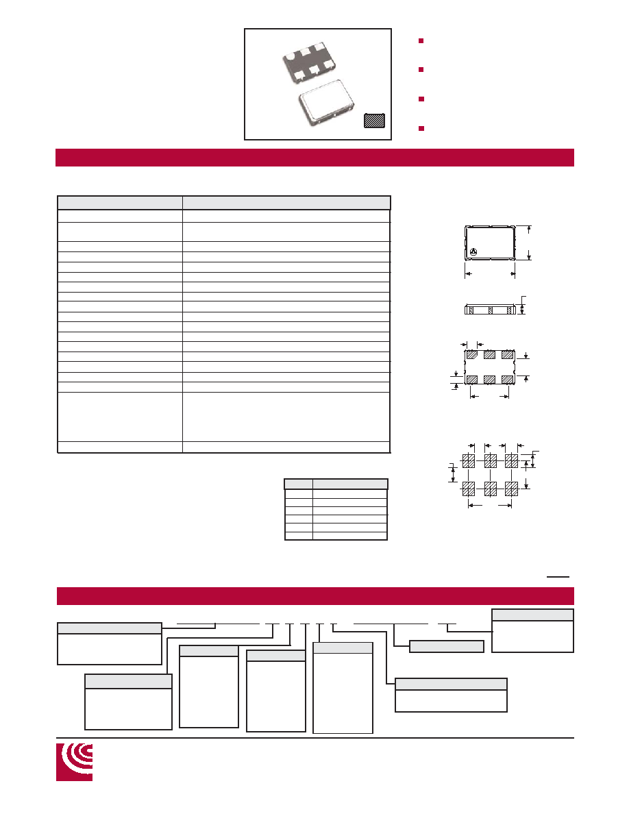
MARKING: See Page 52, Format A
Dimensions: Inches
(mm)
SPECIFICATIONS
Side View
0.75
(1.90)
MAX
Soldering Position
5.08
3.90
1.50
2.40
1.60
0.94
0.197 ±0.008
(5.0 ±0.2)
0.276 ±0.008
(7.0 ±0.2)
1
3
2
4
5
6
4
5
6
3
2
1
0.055
(1.40)
TYP
0.102
(2.60) TYP
0.047
(1.10)
TYP
0.200
(5.08)
TYP
Bottom View
CERAMIC SMD
Miniature, Low Profile
3.3 Vdc Supply Voltage
LVDS
Low Current Consumption
FMVCLVDSC3S
3.3 Vdc LVDS VCXO
CERAMIC SMD 5x7
MARKING: See Page 57, Format M
PART NUMBERING SYSTEM
SERIES
1
Control V
2
Tri-State Control
3
Ground (Case)
4
Output
5
Diff. Output
6
Supply Voltage (Vdd)
Parameter
Specification
All specifications subject to change without notice.
Pin Function
PIN FUNCTION TABLE
Frequency Range
10.000 to 650.000 MHz
Overall Frequency Tolerance
±20 ppm to ±100 ppm
(Inclusive of Operating Temp., Supply Voltage, & Load)
Operating Temperature Range
0 to +70∞C Std., -40 to +85∞C Avail.
Storage Temperature
-55 to +125∞C
Supply Voltage (Vdd)
+3.3 Vdc ± 5%
Supply Current (Icc)
80 mA Typical
Phase Jitter (TpJ)
0.044 x 10
-3
Typical
Phase Jitter (Tp-p)
3 pS RMS max. | Condition: 12 kHz to 20 MHz
Accumulated Jitter (Tacc)
3 pS RMS max. | Condition: 12 kHz to 20 MHz
Symmetry (Duty Cycle)
45/55%
Rise and Fall Time
500 ps Typ. / 800 ps max.
Start Time
10 ms max. < 5 ms typical
Output LVDS
Output Load
100 ohms max. (Vcc - 2.0V)
Differential Output Voltage
0.247V to 0.454V
(Vod) (Out 1 - Out 2)
(0.33V Typical)
Offset Voltage
1.25 Vos
Pin 1 Options
No Connect (Std.)
(See Spec. Option T below)
Tri-State (option T)
VIH: 1.6 V max. or Open Enables Output
VIL: 0.9 V min. Disables Output
Output Disable/Enable Time: 100 nS max.
Aging @ 25∞C
±5ppm max first year
05|issue1|082505
FMVCLVDSC3S 50 C G A L - XX.XXXXXXM - CM
25 - ± 25 ppm
50 - ± 50 ppm
00 - ± 100 ppm
nn - ± Custom Value
Overall Frequency Tol.
Frequency (MHz)
HCMOS/TTL Compatible
3.3 Vdc LVDS VCXO
Ceramic SMD
Product Family
PD - Parameter Data
CM - Custom Mark
BLANK - None Req'd.
Options
A - +1-50 ppm
B - ± 75 ppm
C - ± 100 ppm
D - ± 125 ppm
E - ± 150 ppm
X - Custom
Z - No Spec.
Min. Pullability
C - ± 100 ppm
D - ± 125 ppm
E - ± 150 ppm
F - ± 175 ppm
G - ± 200 ppm
X - Custom
Z - No Spec.
Max. Pullability
L - Linearity ±10% Max.
BLANK- None Required (Std.)
Spec. Options
A 0 to 70 ∞C
B -20 to 70 ∞C
C -40 to 85 ∞C
D -10 to 50 ∞C
E -10 to 60 ∞C
F -30 to 60 ∞C
J
0 to 50 ∞C
X - Custom
Temp. Range
Actual Size