 | –≠–ª–µ–∫—Ç—Ä–æ–Ω–Ω—ã–π –∫–æ–º–ø–æ–Ω–µ–Ω—Ç: FT245BM | –°–∫–∞—á–∞—Ç—å:  PDF PDF  ZIP ZIP |

DS245B Version 1.0 © Future Technology Devices Intl. Ltd. 2002
Page 1 of 22
FT245BM USB FIFO ( USB - Parallel ) I.C.
The FT245BM is the 2
nd
generation of FTDI's popular USB FIFO i.c. This device not only adds extra functionality
to it's FT8U245AM predecessor and reduces external component count, but also maintains a high degree of pin
compatibility with the original, making it easy to upgrade or cost reduce existing designs as well as increasing the
potential for using the device in new application areas.
1.0 Features
HARDWARE FEATURES
∑
Single Chip USB Û Parallel FIFO bi-directional
Data Transfer
∑
Transfer Data rate to 1M Byte / Sec - D2XX Drivers
∑
Transfer Data rate to 3,000 Baud - VCP Drivers
∑
Simple to interface to MCU/ PLD / FPGA logic with
a 4 wire handshake interface
∑
Entire USB protocol handled on-chip ... no USB-
specifi c fi rmware programming required
∑
FTDI's royalty-free VCP and D2XX drivers
eliminate the requirement for USB driver
development in most cases.
∑
384 Byte FIFO Tx buffer / 128 Byte FIFO Rx Buffer
for high data throughput.
∑
New Send Immediate support via SENDI Pin for
optimised data throughput.
∑
Support for USB Suspend / Resume through
PWREN# and WAKEUP pins.
∑
Support for high power USB Bus powered devices
through PWREN# pin
∑
Adjustable RX buffer timeout
∑
In-built support for event characters
∑
Integrated level converter on FIFO and control
signals for interfacing to 5v and 3.3v logic
∑
Integrated 3.3v regulator for USB IO
∑
Integrated Power-On-Reset circuit
∑
Integrated 6MHz ≠ 48Mhz clock multiplier PLL
∑
USB Bulk or Isocronous data transfer modes
∑
New Bit-Bang Mode allows the data bus to be used
as an 8 bit general purpose IO Port without the
need for MCU or other support logic.
∑
4.4v to 5.25v single supply operation
∑
UHCI / OHCI / EHCI host controller compatible
∑
USB 1.1 and USB 2.0 compatible
∑
USB VID, PID , Serial Number and Product
Description strings in external EEPROM
∑
EEPROM programmable on-board via USB
∑
Compact 32LD PQFP package
VIRTUAL COM PORT ( VCP ) DRIVERS for
-
Windows 98 and Windows 98 SE
-
Windows 2000 / ME / XP
-
Windows CE **
-
MAC OS-8 and OS-9
-
MAC OS-X **
-
Linux 2.40 and greater
D2XX ( USB Direct Drivers + DLL S/W Interface )
-
Windows 98 and Windows 98 SE
-
Windows 2000 / ME / XP
APPLICATION AREAS
-
Easy MCU / PLD / FPGA interface to USB
-
Upgrading Legacy Peripheral Designs to USB
-
USB Instrumentation
-
USB Industrial Control
-
USB Audio and Low Bandwidth Video data transfer
-
PDA Û USB data transfer
-
USB MP3 Player Interface
-
USB FLASH Card Reader / Writers
-
Set Top Box ( S.T.B. ) PC - USB interface
-
USB Digital Camera Interface
-
USB Hardware Modems
-
USB Wireless Modems
-
[ ** = In planning or under development ]

DS245B Version 1.0 © Future Technology Devices Intl. Ltd. 2002
Page 2 of 22
FT245BM USB FIFO ( USB - Parallel ) I.C.
2.0 Enhancements
This section summarises the enhancements of the 2
nd
generation device compared to it's FT8U245AM predecessor.
For further details, consult the device pin-out description and functional descriptions.
∑
Integrated Power-On-Reset ( POR ) Circuit
The device now incorporates an internal POR
function. The existing RESET# pin is maintained
in order to allow external logic to reset the device
where required, however for many applications
this pin can now be either left N/C or hard wired to
VCC. In addition, a new reset output pin ( RSTO#
) is provided in order to allow the new POR circuit
to provide a stable reset to external MCU and other
devices. RSTO# was the TEST pin on the previous
generation of devices.
∑
Integrated RCCLK Circuit
In the previous devices, an external RC circuit
was required to ensure that the oscillator and
clock multiplier PLL frequency was stable prior
to enabling the clock internal to the device. This
circuit is now embedded on-chip ≠ the pin assigned
to this function is now designated as the TEST pin
and should be tied to GND for normal operation.
∑
Integrated Level Converter on FIFO interface
and control signals
The previous devices would drive the FIFO and
control signals at 5v CMOS logic levels. The
new device has a separate VCC-IO pin allowing
the device to directly interface to 3.3v and other
logic families without the need for external level
converter i.c.'s
∑
Power Management control for USB Bus
Powered, high current devices
A new PWREN# signal is provided which can be
used to directly drive a transistor or P-Channel
MOSFET in applications where power switching
of external circuitry is required. A new EEPROM
based option makes the device pull gently down
it's FIFO interface lines when the power is shut off
( PWREN# is High ). In this mode, any residual
voltage on external circuitry is bled to GND when
power is removed thus ensuring that external
1.1 General Description
The FT245BM provides an easy cost-effective method of transferring data to / from a peripheral and a
host P.C. at up to 8 Million bits ( 1 Megabyte ) per second. Its simple, FIFO-like design makes it easy to interface to
any microcontroller or microprocessor via IO ports.
To send data from the peripheral to the host computer, simply write the byte-wide data into the module when TXE# is
low. If the (384-byte) transmit buffer fi lls up or is busy storing the previously written byte, the device takes TXE# high in
order to stop further data from being written until some of the FIFO data has been transferred over USB to the host.
When the host sends data to the peripheral over USB, the device will take RXF# low to let the peripheral know that
at least one byte of data is available. The peripheral then reads the data until RXF# goes high indicating that no more
data is available to read.
By using FTDI's virtual COM port drivers, the peripheral looks like a standard COM port to the application software.
Commands to set the baud rate are ignored--the device always transfers data at its fastest rate regardless of the
application's baud-rate setting. Alternatively, FTDI's D2XX drivers allow application software to access the device
"directly" through a published DLL based API. Details of the current VCP and D2XX driver can be found on FTDI's web
site (
http://www.ftdichip.com
)

DS245B Version 1.0 © Future Technology Devices Intl. Ltd. 2002
Page 3 of 22
FT245BM USB FIFO ( USB - Parallel ) I.C.
circuitry controlled by PWREN# resets reliably
when power is restored. PWREN# can also be
used by external circuitry to determine when USB
is in suspend mode ( PWREN# goes high ).
∑
Send Immediate / WakeUp ( SI / WU ) signal
The new Send Immediate / WakeUp signal
combines two functions on a single pin. If USB is
in suspend mode ( and remote wakeup is enabled
in the EEPROM ), strobing this pin low will cause
the device to request a resume from suspend
( WakeUp ) on the USB Bus. Normally, this can
be used to wake up the Host PC. During normal
operation, if this pin is strobed low any data in the
device RX buffer will be sent out over USB on the
next Bulk-IN request from the drivers regardless of
the packet size. This can be used to optimise USB
transfer speed for some applications.
∑
Lower Suspend Current
Integration of RCCLK within the device and internal
design improvements reduce the suspend current
of the FT245BM to under 100uA typical ( excluding
the 1.5k pull-up on USB DP ) in USB suspend
mode. This allows greater margin for peripherals to
meet the USB Suspend current limit of 500uA.
∑
Support for USB Isocronous Transfers
Whilst USB Bulk transfer is usually the best
choice for data transfer, the scheduling time of the
data is not guaranteed. For applications where
scheduling latency takes priority over data integrity
such as transferring audio and low bandwidth
video data, the new device now offers an option
of USB Isocronous transfer via an option bit in the
EEPROM.
∑
Programmable FIFO TX Buffer Timeout
In the previous device, the TX buffer timeout
used to fl ush remaining data from the TX buffer
was fi xed at 16ms timeout. This timeout is now
programmable over USB in 1ms increments
from 1ms to 255ms, thus allowing the device to
be better optimised for protocols requiring faster
response times from short data packets.
∑
Relaxed VCC Decoupling
The 2
nd
generation devices now incorporate a level
of on-chip VCC decoupling. Though this does
not eliminate the need for external decoupling
capacitors, it signifi cantly improves the ease of pcb
design requirements to meet FCC,CE and other
EMI related specifi cations.
∑
Bit Bang Mode
The 2
nd
generation device has a new option
referred to as "Bit Bang" mode. In Bit Bang mode,
the eight FIFO data lines can be switched between
FIFO interface mode and an 8-bit Parallel IO
port. Data packets can be sent to the device and
they will be sequentially sent to the interface at a
rate controlled by an internal timer ( equivalent to
the prescaler of the FT232BM device ). As well
as allowing the device to be used stand-alone
as a general purpose IO controller for example
controlling lights, relays and switches, some other
interesting possibilities exist. For instance, it may
be possible to connect the device to an SRAM
confi gurable FPGA as supplied by vendors such as
Altera and Xilinx. The FPGA device would normally
be un-confi gured ( i.e. have no defi ned function )
at power-up. Application software on the PC could
use Bit Bang Mode to download confi guration
data to the FPGA which would defi ne it's hardware
function, then after the FPGA device is confi gured
the FT245BM can switch back into FIFO interface
mode to allow the programmed FPGA device
to communicate with the PC over USB. This
approach allows a customer to create a "generic"
USB peripheral who's hardware function can be
defi ned under control of the application software.
The FPGA based hardware can be easily upgraded
or totally changed simply by changing the FPGA
confi guration data fi le. Application notes, software
and development modules for this application area
will be available from FTDI and other 3
rd
party
developers.
DS245B Version 1.0 © Future Technology Devices Intl. Ltd. 2002
Page 4 of 22
FT245BM USB FIFO ( USB - Parallel ) I.C.
∑
Less External Support Components
As well as eliminating the RCCLK RC network, and
for most applications the need for an external reset
circuit, we have also eliminated the requirement for
a 100k pull-up on EECS to select 6MHz operation.
When the FT245BM is being used without the
confi guration EEPROM, EECS, EESK and
EEDATA can now be left n/c. For circuits requiring
a long reset time ( where the device is reset
externally using a reset generator i.c., or reset is
controlled by the IO port of a MCU, FPGA or ASIC
device ) an external transistor circuit is no longer
required as the 1k5 pull-up resistor on USB DP can
be wired to the RESETO# pin instead of to 3.3v.
Note : RESETO# drives out at 3.3v level, not at 5v
VCC level. This is the preferred confi guration for
new designs. In some other confi gurations, RSTO#
can be used to reset external logic / MCU circuitry.
∑
Extended EEROM Support
The previous generation of devices only supported
EEPROM of type 93C46 ( 128 x 16 bit ). The new
devices will also work with EEPROM type 93C56
( 256 x 16 bit ) and 93C66 ( 512 x 16 bit ). The
extra space is not used by the device, however it
is available for use by other external MCU / logic
whilst the FT245BM is being held in reset.
∑
USB 2.0 ( full speed option )
A new EEPROM based option allows the FT245BM
to return a USB 2.0 device descriptor as opposed
to USB 1.1. Note : The device would be a USB 2.0
Full Speed device ( 12Mb/s ) as opposed to a USB
2.0 High Speed device ( 480Mb/s ).
∑
Multiple Device Support without EEPROM
When no EEPROM ( or a blank or invalid
EEPROM ) is attached to the device, the FT245BM
no longer gives a serial number as part of it's
USB descriptor. This allows multiple devices to
be simultaneously connected to the same PC.
However, we still highly recommend that EEPROM
is used, as without serial numbers a device can
only be identifi ed by which hub port in the USB tree
it is connected to which can change if the end user
re-plugs the device into a different port.
∑
EEREQ# / EEGNT#
These ( FT8U245AM ) pins are not supported on
the FT245BM device. They have been replaced
with the new SI / WU and PWREN# signals
respectively.
DS245B Version 1.0 © Future Technology Devices Intl. Ltd. 2002
Page 5 of 22
FT245BM USB FIFO ( USB - Parallel ) I.C.
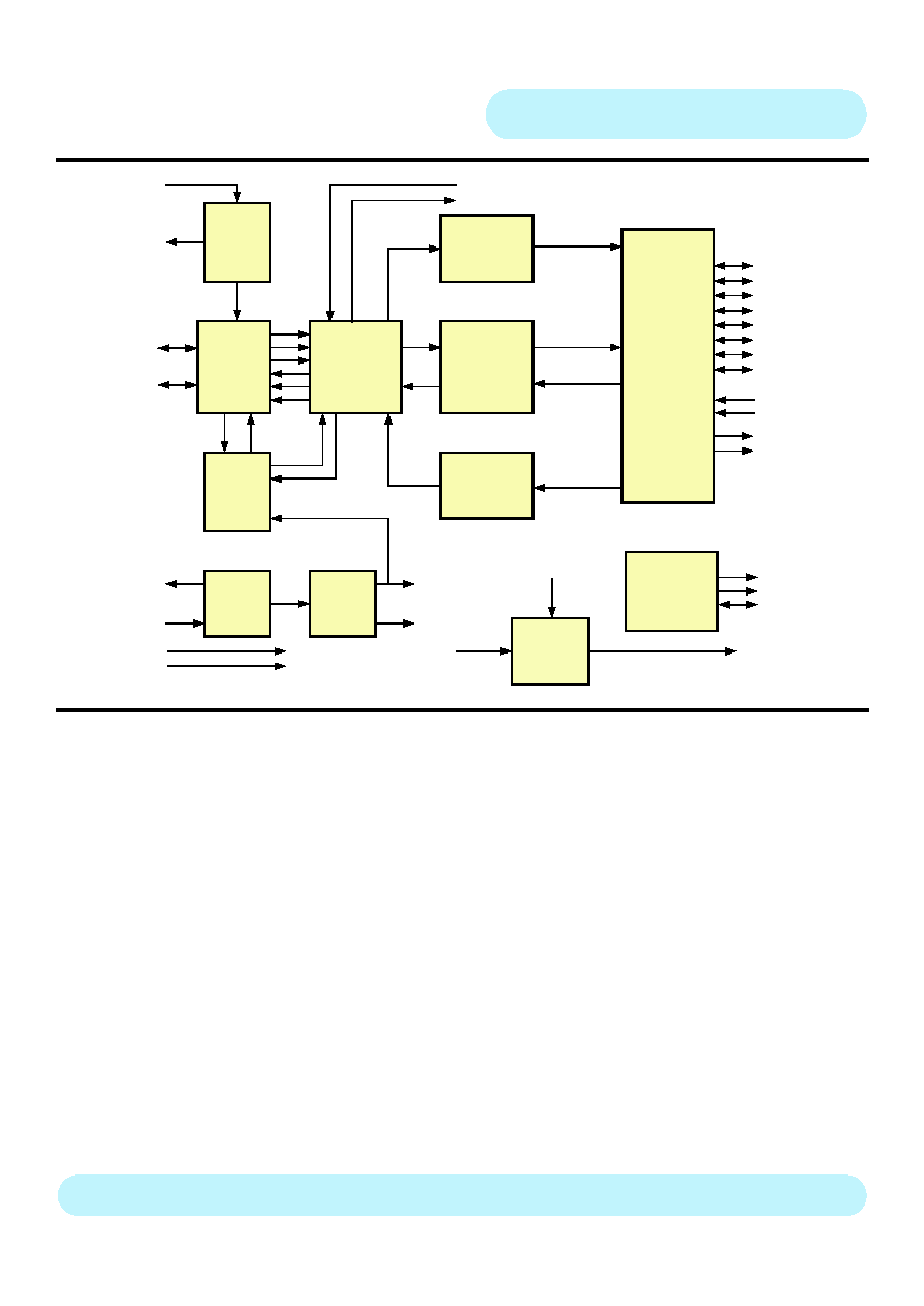
3.0 Block Diagram ( simplifi ed )
x8 Clock
Multiplier
Serial Interface
Engine
( SIE )
USB
Protocol Engine
FIFO Transmit
Buffer
384 Bytes
FIFO Receive
Buffer
128 Bytes
3.3 Volt
LDO
Regulator
USB
Transceiver
USB DPLL
6MHZ
Oscillator
48MHz
12MHz
XTIN
XTOUT
USBDP
USBDM
3V3OUT
VCC
RESET#
TEST
GND
FIFO
Controller
D0
D1
D2
D3
D4
D5
D6
D7
EEPROM
Interface
RD#
WR
EECS
EESK
EEDATA
RXF#
TXE#
PWREN#
RESET
GENERATOR
RSTOUT#
3V3OUT
Send Immediate / WakeUP
3.1 Functional Block Descriptions
∑
3.3V LDO Regulator
The 3.3V LDO Regulator generates the 3.3 volt
reference voltage for driving the USB transceiver
cell output buffers. It requires an external
decoupling capacitor to be attached to the 3V3OUT
regulator output pin. It also provides 3.3v power to
the RSTOUT# pin. The main function of this block
is to power the USB Transceiver and the Reset
Generator Cells rather than to power external logic.
However, external circuitry requiring 3.3v nominal
at a current of not greater than 5mA could also
draw it's power from the 3V3OUT pin if required.
∑
USB Transceiver
The USB Transceiver Cell provides the USB 1.1 /
USB 2.0 full-speed physical interface to the USB
cable. The output drivers provide 3.3 volt level slew
rate control signalling, whilst a differential receiver
and two single ended receivers provide USB data
in, SEO and USB Reset condition detection.
∑
USB DPLL
The USB DPLL cell locks on to the incoming NRZI
USB data and provides separate recovered clock
and data signals to the SIE block.
∑
6MHz Oscillator
The 6MHz Oscillator cell generates a 6MHz
reference clock input to the X8 Clock multiplier
from an external 6MHz crystal or ceramic
resonator.
∑
x8 Clock Multiplier
The x8 Clock Multiplier takes the 6MHz input
from the Oscillator cell and generates a 12MHz
reference clock for the SIE, USB Protocol Engine
and FIFO FIFO controller blocks. It also generates
a 48MHz reference clock for the USB DPLL.
∑
Serial Interface Engine ( SIE )
The Serial Interface Engine ( SIE ) block performs
the Parallel to Serial and Serial to Parallel
conversion of the USB data. In accordance to the