IGBT MODULE ( N series )
n
n
Features
∑ Square RBSOA
∑ Low Saturation Voltage
∑ Less Total Power Dissipation
∑ Improved FWD Characteristic
∑ Minimized Internal Stray Inductance
∑ Overcurrent Limiting Function (~3 Times Rated Current)
n
n
Applications
∑ High Power Switching
∑ A.C. Motor Controls
∑ D.C. Motor Controls
∑ Uninterruptible Power Supply
n
n
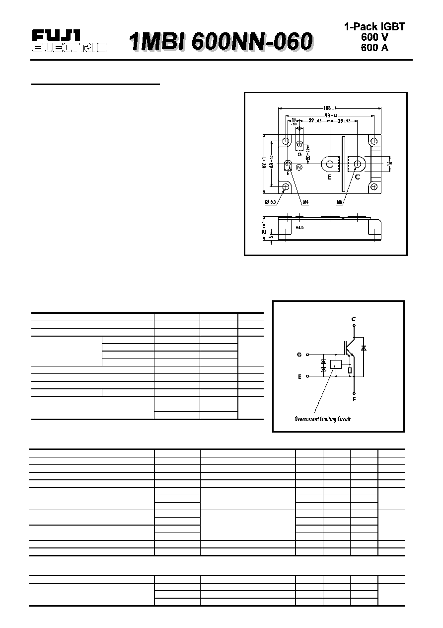
Outline Drawing
n
n
Maximum Ratings and Characteristics
∑
Absolute Maximum Ratings
( T
c
=25∞C
)
Items
Symbols
Ratings
Units
Collector-Emitter Voltage
V
CES
600
V
Gate -Emitter Voltage
V
GES
±
20
V
Continuous
I
C
600
Collector
1ms
I
C PULSE
1200
Current
Continuous
-I
C
600
1ms
-I
C PULSE
1200
Max. Power Dissipation
P
C
2000
W
Operating Temperature
T
j
+150
∞C
Storage Temperature
T
stg
-40
+125
∞C
Isolation Voltage
A.C. 1min.
V
is
2500
V
Mounting *1
3.5
Screw Torque
Terminals *2
4.5
Nm
Terminals *3
1.7
Note: *1:Recommendable Value; 2.5
3.5 Nm (M5) or (M6)
*2:Recommendable Value; 3.5
4.5 Nm (M6)
*3:Recommendable Value; 1.3
1.7 Nm (M4)
∑
Electrical Characteristics
( at T
j
=25∞C )
Items
Symbols
Test Conditions
Min.
Typ.
Max.
Units
Zero Gate Voltage Collector Current
I
CES
V
GE
=0V V
CE
=600V
4.0
mA
Gate-Emitter Leackage Current
I
GES
V
CE
=0V V
GE
=
±
20V
60
µ
A
Gate-Emitter Threshold Voltage
V
GE(th)
V
GE
=20V I
C
=600mA
4.5
7.5
V
Collector-Emitter Saturation Voltage
V
CE(sat)
V
GE
=15V I
C
=600A
2.8
V
Input capacitance
C
ies
V
GE
=0V
39600
Output capacitance
C
oes
V
CE
=10V
8800
pF
Reverse Transfer capacitance
C
res
f=1MHz
4000
t
ON
V
CC
=300V
0.6
1.2
t
r
I
C
=600A
0.2
0.6
t
OFF
V
GE
=
±
15V
0.6
1.0
t
f
R
G
=2.7
0.2
0.35
Diode Forward On-Voltage
V
F
I
F
=600A V
GE
=0V
3.0
V
Reverse Recovery Time
t
rr
I
F
=600A
300
ns
∑
Thermal Characteristics
Items
Symbols
Test Conditions
Min.
Typ.
Max.
Units
R
th(j-c)
IGBT
0.063
Thermal Resistance
R
th(j-c)
Diode
0.11
∞C/W
R
th(c-f)
With Thermal Compound
0.0125
n
Equivalent Circuit
Turn-on Time
Turn-off Time
µ
s
A
0
200
400
600
800
1000
10
100
1000
t
f
t
r
t
off
t
on
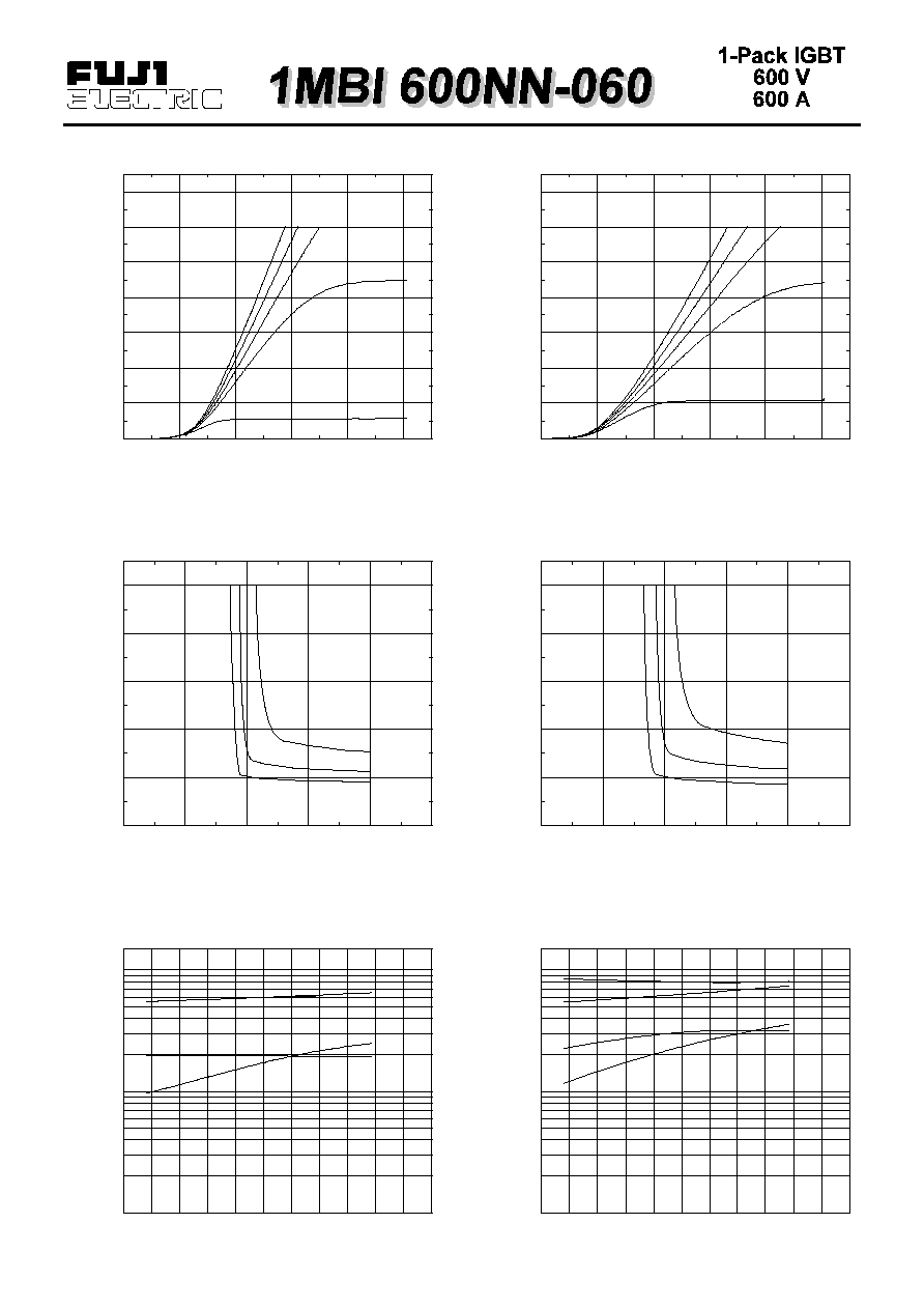
Switching time vs. Collector current
V
CC
=300V, R
G
=2.7
, V
GE
±15V, T
j
=25∞C
Switching time : t
on
, t
r
, t
off
, t
f
[nsec]
Collector current : I
C
[A]
0
1
2
3
4
5
0
200
400
600
800
1000
1200
1400
10V
V
GE
=20V,15V,12V,
Collector-Emitter voltage : V
CE
[V]
Collector current : I
C
[A]
8V
Collector current vs. Collector-Emitter voltage
T
j
=125∞C
0
1
2
3
4
5
0
200
400
600
800
1000
1200
1400
Collector current vs. Collector-Emitter voltage
T
j
=25∞C
Collector current : I
C
[A]
Collector-Emitter voltage : V
CE
[V]
8V
10V
V
GE
=20V,15V,12V
0
5
10
15
20
25
0
2
4
6
8
10
Collector-Emitter vs. Gate-Emitter voltage
T
j
=25∞C
300A
600A
1200A
I
C
=
Collector-Emitter voltage :V
CE
[V]
Gate-Emitter voltage : V
GE
[V]
0
5
10
15
20
25
0
2
4
6
8
10
Collector-Emitter vs. Gate-Emitter voltage
T
j
=125∞C
300A
600A
1200A
I
C
=
Collector-Emitter voltage V
CE
[V]
Gate-Emitter voltage : V
GE
[V]
0
200
400
600
800
1000
10
100
1000
Switching time vs. Collector current
V
CC
=300V, R
G
=2.7
, V
GE
=±15V, T
j
=125∞C
t
f
t
r
t
on
t
off
Switching time : t
on
, t
r
, t
off
, t
f
[nsec]
Collector current : I
C
[A]
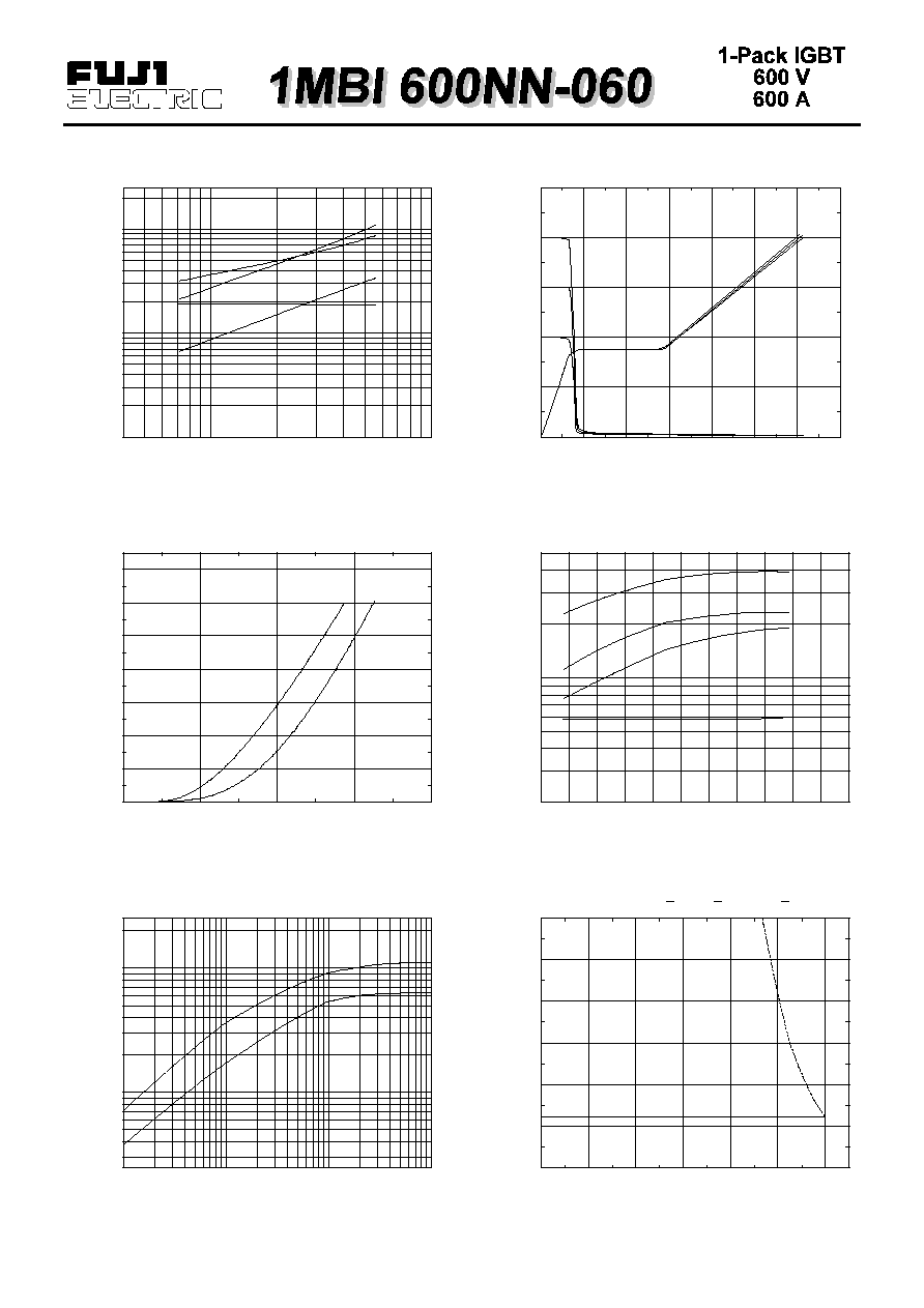
0 , 0 0 1
0,01
0,1
1
0,01
0,1
I G B T
D i o d e
T r a n s i e n t t h e r m a l r e s i s t a n c e
Thermal resistance : R
th(j-c)
[∞C/W]
P u l s e w i d t h : P W [ s e c ]
0
5 0 0
1 0 0 0
1 5 0 0
2 0 0 0
2 5 0 0
3 0 0 0
3 5 0 0
0
1 0 0
2 0 0
3 0 0
4 0 0
5 0 0
4 0 0 V
3 0 0 V
V
C C
= 2 0 0 V
0
5
1 0
1 5
2 0
2 5
D y n a m i c i n p u t c h a r a c t e r i s t i c s
T
j
= 2 5 ∞ C
Collector-Emitter voltage : V
CE
[V]
G a t e c h a r g e : Q
G
[ n C ]
1
1 0
1 0
1 0 0
1 0 0 0
tf
tr
toff
ton
S w i t c h i n g t i m e v s . R
G
V
C C
= 3 0 0 V , I
C
= 6 0 0 A , V
G E
= ± 1 5 V , T
j
= 2 5 ∞ C
Switching time : t
on
, t
r
, t
off
, t
f
[nsec]
G a t e r e s i s t a n c e : R
G
[
]
0
1
2
3
4
0
2 0 0
4 0 0
6 0 0
8 0 0
1 0 0 0
1 2 0 0
1 4 0 0
T
j
= 1 2 5 ∞ C 2 5 ∞ C
F o r w a r d c u r r e n t v s . F o r w a r d v o l t a g e
V
G E
= O V
Forward current : I
F
[A]
F o r w a r d v o l t a g e : V
F
[V]
0
2 0 0
4 0 0
6 0 0
8 0 0
1 0 0 0
1 0 0
I
rr
2 5 ∞ C
t
rr
2 5 ∞ C
t
rr
1 2 5 ∞ C
I
rr
1 2 5 ∞ C
R e v e r s e r e c o v e r y c h a r a c t e r i s t i c s
t
rr
, I
rr
v s . I
F
Reverse recovery current : I
rr
[A]
Reverse recovery time : t
rr
[nsec]
F o r w a r d c u r r e n t : I
F
[A]
0
1 0 0
2 0 0
3 0 0
4 0 0
5 0 0
6 0 0
0
1 0 0 0
2 0 0 0
3 0 0 0
4 0 0 0
5 0 0 0
6 0 0 0
R B S O A ( R e p e t i t i v e p u l s e )
S C S O A
(non-repetitive pulse)
R e v e r s e d b i a s e d s a f e o p e r a t i n g a r e a
+ V
G E
= 1 5 V , - V
G E
< 1 5 V , T
j
< 1 2 5 ∞ C , R
G
> 2.7
Collector current : I
C
[A]
Collector-Emitter voltage : V
C E
[V]
Gate-Emitter Voltage : V
GE
[V]
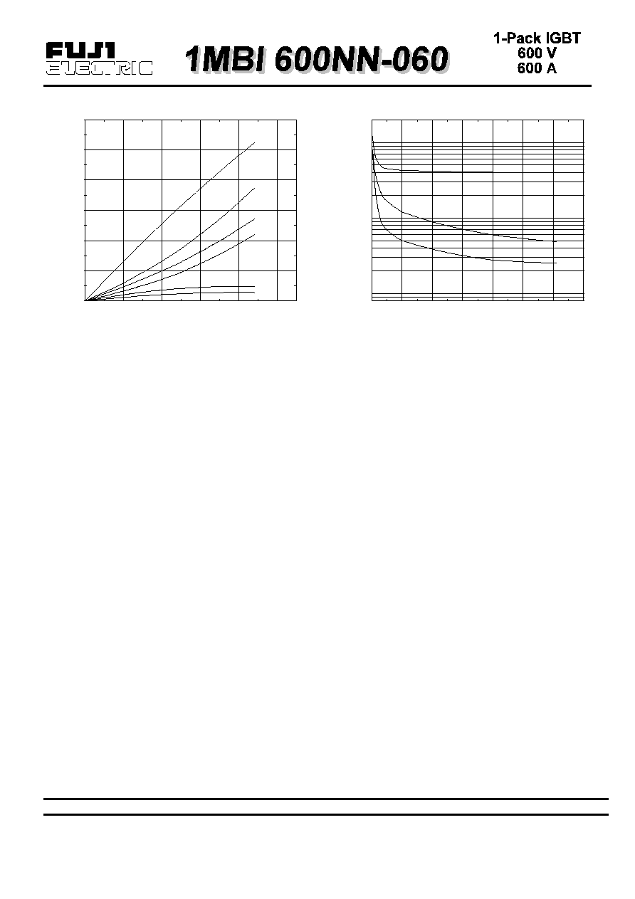
0 5 1 0 1 5 2 0 2 5 3 0 3 5
1
1 0
1 0 0
C
res
C
oes
C
ies
Capacitance vs. Collector-Emitter voltage
T
j
=25∞C
Capacitance : C
ies
, C
oes
, C
res
[nF]
Collector-Emitter Voltage : V
CE
[V]
0 2 0 0 4 0 0 6 0 0 8 0 0 1 0 0 0
0
1 0
2 0
3 0
4 0
5 0
6 0
E
rr
25∞C
E
rr
125∞C
Switching loss vs. Collector current
V
CC
=300V, R
G
=2.7
, V
GE
=±15V
Switching loss : E
on
, E
off
, E
rr
[mJ/cycle]
Collector Current : I
C
[A]
E
on
25∞C
E
on
125∞C
E
off
25∞C
E
off
125∞C
Fuji Electric GmbH Fuji Electric (UK) Ltd.
Lyoner Straþe 26 Commonwealth House
2 Chalkhill Road Hammersmith
D-60528 Frankfurt/M London W6 8DW, UK
Tel.: 069 - 66 90 29 - 0 Tel.: 0181 - 233 11 30
Fax.: 069 - 66 90 29 - 56 Fax.: 0181 - 233 11 60
P.O. Box 702708-Dallas, TX 75370 Phone (972) 233-1589 Fax (972) 233-0481 www.collmer.com