
2MBI200NB-120-01
IGBT Module
1200V / 200A 2 in one-package
Features
∑ VCE(sat) classified for easy parallel connection
∑ High speed switching
∑ Voltage drive
∑ Low inductance module structure
Applications
∑ Inverter for Motor drive
∑ AC and DC Servo drive amplifier
∑ Uninterruptible power supply
∑ Industrial machines, such as Welding machines
Maximum ratings and characteristics
Absolute maximum ratings
(at Tc=25∞C unless otherwise specified)
Item Symbol
Collector-Emitter voltage V
CES
Gate-Emitter voltage V
GES
Collector Continuous I
C
current 1ms I
C
pulse
-I
C
1ms -I
C
pulse
Max. power dissipation P
C
Operating temperature T
j
Storage temperature T
stg
Isolation voltage V
is
Screw torque Mounting *
1
Terminals *
2
Rating
1200
±20
200
400
200
400
1500
+150
-40 to +125
AC 2500 (1min.)
3.5
4.5
Unit
V
V
A
A
A
A
W
∞C
∞C
V
N∑m
N∑m
Item Symbol Characteristics Conditions Unit
Min. Typ. Max.
Zero gate voltage collector current
Gate-Emitter leakage current
Gate-Emitter threshold voltage
Collector-Emitter saturation voltage
Input capacitance
Output capacitance
Reverse transfer capacitance
Turn-on time
Turn-off time
Diode forward on voltage
Reverse recovery time
I
CES
I
GES
V
GE(th)
V
CE(sat)
C
ies
C
oes
C
res
t
on
t
r
t
off
t
f
V
F
t
rr
≠ ≠ 2.0
≠ ≠ 30
4.5 ≠ 7.5
≠ ≠ 3.3
≠ 32000 ≠
≠ 11600 ≠
≠ 10320 ≠
≠ 0.65 1.2
≠ 0.25 0.6
≠ 0.85 1.5
≠ 0.35 0.5
≠ ≠ 3.0
≠ ≠ 0.35
V
GE
=0V, V
CE
=1200V
V
CE
=0V, V
GE
=±20V
V
CE
=20V, I
C
=200mA
V
GE
=15V, I
C
=200A
V
GE
=0V
V
CE
=10V
f=1MHz
V
CC
=600V
I
C
=200A
V
GE
=±15V
R
G
=4.7ohm
I
F
=200A, V
GE
=0V
I
F
=200A
mA
µA
V
V
pF
µs
V
µs
Electrical characteristics (at Tj=25∞C unless otherwise specified)
Thermal resistance characteristics
Item Symbol Characteristics Conditions Unit
Min. Typ. Max.
Rth(j-c)
Thermal resistance Rth(j-c)
Rth(c-f)*
≠ ≠ 0.085
≠ ≠ 0.18
≠ 0.025 ≠
IGBT
Diode
the base to cooling fin
∞C/W
∞C/W
∞C/W
* :
This is the value which is defined mounting on the additional cooling fin with thermal compound
Equivalent Circuit Schematic
§ Current control circuit
G1 E1 G2 E2
C1
E2
C2E1
§
§
*
1 :
Recommendable value : 2.5 to 3.5 N∑m (M5) or (M6)
*
2 :
Recommendable value : 3.5 to 4.5 N∑m (M6)
V
CE(sat)
classification
Rank Lenge Conditions
F 2.25 to 2.50V
A 2.40 to 2.65V Ic = 200A
B 2.55 to 2.80V V
GE
= 15V
C 2.70 to 2.95V Tj = 25∞C
D 2.85 to 3.10V
E 3.00 to 3.30V

2MBI200NB-120-01
IGBT Module
Characteristics (Representative)
Collector current vs. Collector-Emitter voltage
Tj=25∞C
Collector current vs. Collector-Emitter voltage
Tj=125∞C
Collector-Emitter vs. Gate-Emitter voltage
Tj=25∞C
Collector-Emitter vs. Gate-Emitter voltage
Tj=125∞C
Switching time vs. Collector current
Vcc=600V, RG=4.7 ohm, VGE=±15V, Tj=25∞C
Switching time vs. Collector current
Vcc=600V, RG=4.7 ohm, VGE=±15V, Tj=125∞C
Collector-Emitter voltage : VCE [V]
Collector-Emitter voltage : VCE [V]
Collector current : Ic [A]
Collector current : Ic [A]
500
400
300
200
100
0
500
400
300
200
100
0
0 1 2 3 4 5
0 1 2 3 4 5
Collector-Emitter v
oltage :
VCE [V]
Collector-Emitter v
oltage :
VCE [V]
10
8
6
4
2
0
0 5 10 15 20 25
0 5 10 15 20 25
10
8
6
4
2
0
Gate-Emitter voltage : VGE [V]
Gate-Emitter voltage : VGE [V]
Switching time :
ton, tr
, toff
, tf [n sec.]
1000
100
10
0 100 200 300 400
Collector current : Ic [A]
0 100 200 300 400
Collector current : Ic [A]
Switching time :
ton, tr
, toff
, tf [n sec.]
1000
100
10

2MBI200NB-120-01
IGBT Module
Switching time vs. RG
Vcc=600V, Ic=200A, VGE=±15V, Tj=25∞C
Dynamic input characteristics
Tj=25∞C
Gate resistance : RG [ohm]
10
Gate charge : Qg [nC]
0 500 1000 1500 2000 2500
100
1000
1000
800
600
400
200
0
Switching time :
ton, tr
, toff
, tf [n sec.]
Collector-Emitter v
o
ltage :
VCE [V]
F
orward current :
IF [A]
500
400
300
200
100
0
0 1 2 3 4 5
Gate-Emitter v
oltage :
V
GE [V]
0
5
10
15
20
25
Forward voltage : VF [V]
Re
v
erse reco
v
e
r
y
current :
Irr [A]
Re
v
erse reco
v
e
r
y
time :
trr [n sec.]
Forward current vs. Forward voltage
VGE=0V
Reverse recovery characteristics
trr, Irr, vs. IF
Forward current : IF [A]
100
Ther
mal resistance :
Rth (j-c) [∞C/W]
Transient thermal resistance
0.01
0.1
0.001 0.01 0.1 1
Pulse width : PW [sec.]
Reversed biased safe operating area
+VGE=15V, -VGE = 15V, Tj = 125∞C, RG = 4.7ohm
0 100 200 300 400
<
<
>
2000
1600
1200
400
0
0 200 400 600 800 1000 1200
Collector-Emitter voltage : VCE [V]
Collector current : Ic [A]
0.001
800
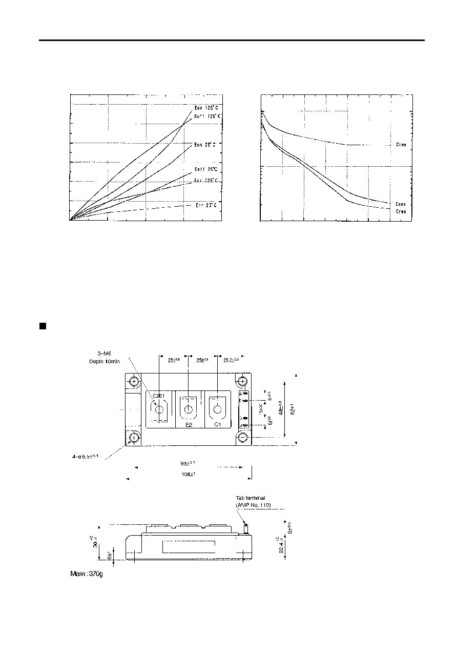
2MBI200NB-120-01
IGBT Module
Outline Drawings, mm
Switching loss vs. Collector current
Vcc=600V, RG=4.7 ohm, VGE=±15V
Switching loss :
Eon, Eoff
, Err [mJ/cycle]
Collector current : Ic [A]
0
10
20
60
0 100 200 300 400
Collector-Emitter voltage : VCE [V]
0 5 10 15 20 25 30 35
1
10
100
Capacitance :
Cies, Coes
, Cres [nF]
Capacitance vs. Collector-Emitter voltage
Tj=25∞C
50
40
30