
2SK1277
N-channel MOS-FET
F-V Series
250V
0,12
30A 150W
> Features > Outline Drawing
-
Include Fast Recovery Diode
-
High Voltage
-
Low Driving Power
> Applications
-
Motor Control
-
Inverters
-
Choppers
> Maximum Ratings and Characteristics > Equivalent Circuit
-
Absolute Maximum Ratings (T
C
=25∞C),
unless otherwise specified
Item Symbol Rating Unit
Drain-Source-Voltage V
DS
250 V
Continous Drain Current I
D
30 A
Pulsed Drain Current I
D(puls)
120 A
Continous Reverse Drain Current I
DR
30 A
Gate-Source-Voltage V
GS
±20 V
Max. Power Dissipation P
D
150 W
Operating and Storage Temperature Range T
ch
150 ∞C
T
stg
-55 ~ +150 ∞C
-
Electrical Characteristics (T
C
=25∞C),
unless otherwise specified
Item Symbol Test conditions Min. Typ. Max. Unit
Drain-Source Breakdown-Voltage V
(BR)DSS
I
D
=1mA V
GS
=0V 250 V
Gate Threshhold Voltage V
GS(th)
I
D
=10mA V
DS=
V
GS
2,1 3,0 4,0 V
Zero Gate Voltage Drain Current I
DSS
V
DS
=250V T
ch
=25∞C 10 500 µA
V
GS
=0V
Gate Source Leakage Current I
GSS
V
GS
=±20V V
DS
=0V 10 100 nA
Drain Source On-State Resistance R
DS(on)
I
D
=15A V
GS
=10V 0,09 0,12
Forward Transconductance g
fs
I
D
=15A V
DS
=25V 10 20 S
Input Capacitance C
iss
V
DS
=25V 2400 3600 pF
Output Capacitance C
oss
V
GS
=0V 500 750 pF
Reverse Transfer Capacitance C
rss
f=1MHz 280 420 pF
Turn-On-Time t
on
(t
on
=t
d(on)
+t
r
) t
d(on)
V
CC
=150V 35 50 ns
t
r
I
D
=30A 140 210 ns
Turn-Off-Time t
off
(t
on
=t
d(off)
+t
f
) t
d(off)
V
GS
=10V 420 630 ns
t
f
R
GS
=25
180 270 ns
Diode Forward On-Voltage V
SD
I
F
=I
DR
V
GS
=0V T
ch
=25∞C 0,9 1,8 V
Reverse Recovery Time t
rr
I
F
=I
DR
V
GS
=0V 100 150 ns
-dI
F
/dt=100A/µs T
ch
=25∞C
- Thermal Characteristics
Item Symbol Test conditions Min. Typ. Max. Unit
Thermal Resistance R
th(ch-a)
channel to air 35 ∞C/W
R
th(ch-c)
channel to case 0,83 ∞C/W
Collmer Semiconductor, Inc. - P.O. Box 702708 - Dallas, TX -75370 - 972-233-1589 - FAX 972-233-0481 - http://www.collmer.com
N-channel MOS-FET
2SK1277
250V
0,12
30A
150W
F-V Series
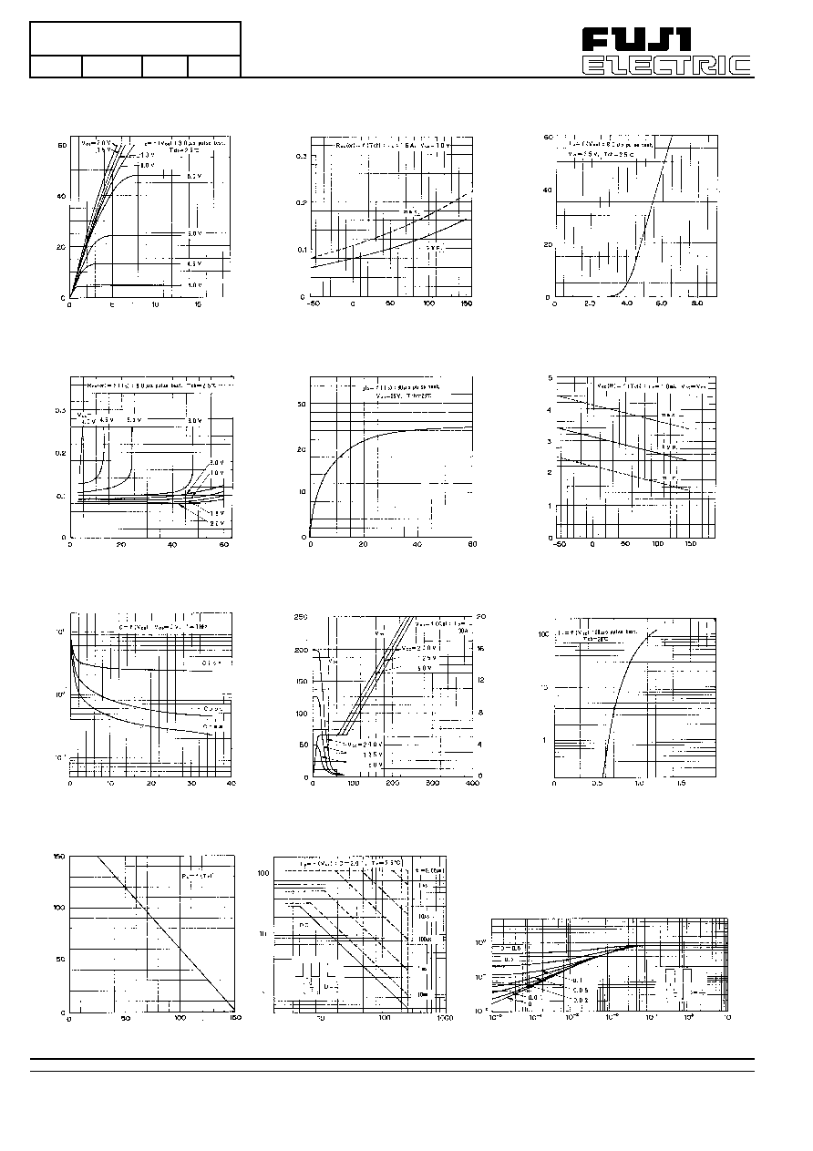
> Characteristics
Typical Output Characteristics
Drain-Source-On-State Resistance vs. T
ch
Typical Transfer Characteristics
1
2
3
I
D
[A]
R
DS(ON)
[
]
I
D
[A]
V
DS
[V]
T
ch
[∞C]
V
GS
[V]
Typical Drain-Source-On-State-Resistance vs. I
D
Typical Forward Transconductance vs. I
D
Gate Threshold Voltage vs. T
ch
4
4
5
6
R
DS(ON)
[
]
g
fs
[S]
V
GS(th)
[V]
I
D
[A]
I
D
[A]
T
ch
[∞C]
Typical Capacitance vs. V
DS
Typical Input Charge
Forward Characteristics of Reverse Diode
7
8
9
C [nF]
V
DS
[V]
V
GS
[V]
I
F
[A]
V
DS
[V]
Q
g
[nC]
V
SD
[V]
Allowable Power Dissipation vs. T
C
Safe operation area
Z
th(ch-c)
[K/W]
Transient Thermal impedance
10
12
11
P
D
[W]
I
D
[A]
T
c
[∞C]
V
DS
[V]
t [s]
This specification is subject to change without notice!