
1
Item
Symbol
Rating
Unit
Drain-source voltage
V
DS
250
Continuous drain current
I
D
18
Pulsed drain current
I
D(puls]
72
Continuous reverse drain current
I
DR
18
Gate-source peak voltage
V
GS
�30
Max. power dissipation
P
D
80
Operating and storage
T
ch
+150
temperature range
T
stg
2SK2254-01L,S
FUJI POWER MOSFET
N-CHANNEL SILICON POWER MOSFET
Equivalent circuit schematic
Maximum ratings and characteristics
Absolute maximum ratings (Tc=25�C unless otherwise specified)
V
A
A
A
V
W
�C
�C
-55 to +150
FAP-IIA SERIES
Electrical characteristics (T
c
=25�C unless otherwise specified)
Thermal characteristics
Item
Symbol
Test Conditions
Zero gate voltage drain current I
DSS
Min. Typ. Max. Units
V
V
�A
mA
nA
S
pF
ns
A
V
ns
�
C
Min. Typ. Max. Units
Thermal resistance
R
th(ch-a)
channel to ambient
R
th(ch-c)
channel to case
125
1.56
�C/W
�C/W
Symbol
V
(BR)DSS
V
GS(th)
I
GSS
R
DS(on)
g
fs
C
iss
C
oss
C
rss
t
d(on)
t
r
t
d(off)
t
f
I
AV
V
SD
t
rr
Q
rr
Item
Drain-source breakdown voltage
Gate threshold voltage
Gate-source leakage current
Drain-source on-state resistance
Forward transconductance
Input capacitance
Output capacitance
Reverse transfer capacitance
Turn-on time t
on
(t
on
=t
d(on)
+t
r
)
Turn-off time t
off
(t
off
=t
d(off)
+t
f
)
Avalanche capability
Diode forward on-voltage
Reverse recovery time
Reverse recovery charge
Test Conditions
I
D
=1mA V
GS
=0V
I
D
=1mA V
DS
=V
GS
V
DS
=250V V
GS
=0V T
ch
=25�C
T
ch
=125�C
V
GS
=�30V V
DS
=0V
I
D
=9A V
GS
=10V
I
D
=9A V
DS
=25V
V
DS
=25V
V
GS
=0V
f=1MHz
V
CC
=150V R
G
=10
I
D
=18A
V
GS
=10V
L=100�H T
ch
=25�C
I
F
=2xI
DR
V
GS
=0V T
ch
=25�C
I
F
=I
DR
V
GS
=0V
-di/dt=100A/
�
s T
ch
=25�C
250
2.5
3.0
3.5
10
500
0.2
1.0
10
100
0.13
0.18
7.0
14.0
1750
2650
290
440
65
100
30
45
50
75
80
120
70
110
18
1.0
1.5
150
1.0
Gate(G)
Source(S)
Drain(D)
Outline Drawings
Features
High speed switching
Low on-resistance
No secondary breakdown
Low driving power
High voltage
V
GS
=
�
30V Guarantee
Avalanche-proof
Applications
Switching regulators
UPS
DC-DC converters
General purpose power amplifier
1. Gate
2, 4. Drain
3. Source
L-type
S-type
EIAJ
�
0.5
�
0.3
�
0.3
�
0.2
�
0.2
+0.2
--0.1
4.5
1.32
2.7
5.08
1.2
10
0.4
0.8
0.9
9.3
1.5
3.0
1. Gate
2, 4. Drain
3. Source
+0.5
+0.2
Max
2
Characteristics
2SK2254-01L,S
FUJI POWER MOSFET
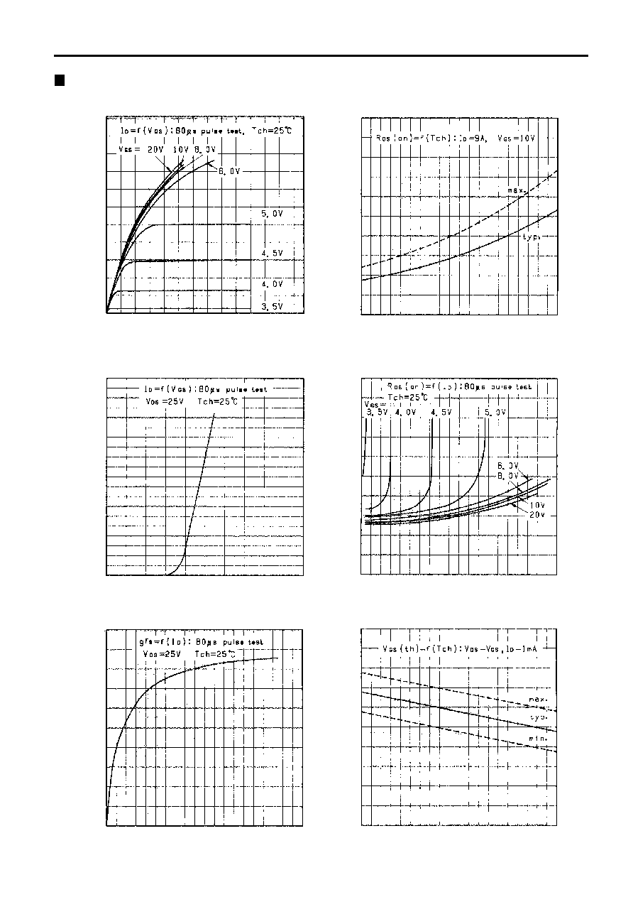
Typical output characteristics
V
DS
[ V ]
I
D
[ A ]
On state resistance vs. T
ch
R
DS(on)
[
]
T
ch
[ �C ]
Typical transfer characteristics
V
GS
[ V ]
I
D
[ A ]
Typical Drain-Source on state resistance vs. I
D
I
D
[ A ]
R
DS(on)
[
]
Typical forward transconductance vs. I
D
I
D
[ A ]
gfs
[ S ]
Gate threshold voltage vs. T
ch
T
ch
[ �C ]
V
GS(th)
[ V ]
-50 0 50 100 150
0 10 20 30 40
50
40
30
20
10
0
0 10 20
0.5
0.4
0.3
0.2
0.1
0
0 2 4 6 8 10
-50 0 50 100 150
0 10 20 30 40
20
16
12
8
4
0
40
30
20
10
0
5
4
3
2
1
0
0.5
0.4
0.3
0.2
0.1
0

3
FUJI POWER MOSFET
Typical capacitance vs. V
DS
V
DS
[ V ]
C
[nF]
Forward characteristics of reverse diode
V
SD
[ V ]
I
F
[ A ]
Allowable power dissipation vs. T
c
T
c
[ �C ]
P
D
[ W ]
Transient thermal impedance
t
[ sec. ]
R
th
[�C/W]
Safe operating area
I
D
[ A ]
V
DS
[ V ]
Typical input charge
V
DS
[ V ]
Qg
[ nC ]
V
GS
[ V ]
0 0.5 1.0 1.5
0 20 40 60 80 100
2SK2254-01L,S
0 10 20 30 40
200
100
0
20
10
0
100
80
60
40
20
0
10
0
10
-1
10
-2
10
-5
10
-4
10
-3
10
-2
10
-1
10
0
10
1
10
1
10
0
10
-1
10
-2
10
2
10
1
10
0
10
-1
10
-2
0 50 100 150
10
0
10
1
10
2
10
3
10
2
10
1
10
0
10
-1
10
-2