1
T-pack (L)
T-pack (S)
Item
Symbol
Ratings
Unit
Drain-source voltage
V
DS
800
Continuous drain current
I
D
±4
Pulsed drain current
I
D(puls]
±16
Gate-source voltage
V
GS
±35
Repetitive or non-repetitive
I
AR *2
4
Maximum Avalanche Energy
E
AS *1
254
Max. power dissipation
P
D
80
Operating and storage
T
ch
+150
temperature range
T
stg
Electrical characteristics (T
c
=25∞C unless otherwise specified)
Thermalcharacteristics
2SK2762-01L,S
FUJI POWER MOSFET
N-CHANNEL SILICON POWER MOSFET
FAP-2S Series
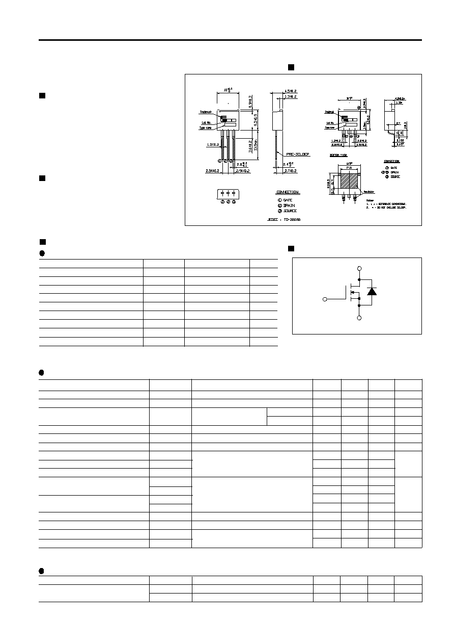
Equivalent circuit schematic
Maximum ratings and characteristic
Absolute maximum ratings
(Tc=25∞C unless otherwise specified)
Item
Symbol Test Conditions
Zero gate voltage drain current I
DSS
V
DS
=800V
V
GS
=±35V
I
D
=2.0A V
GS
=10V
I
D
=2.0A V
DS
=25V
V
CC
=600V I
D
=4A
V
GS
=10V
R
GS
=10
Min. Typ. Max. Units
V
V
µA
mA
nA
S
pF
A
V
ns
µC
ns
Min. Typ. Max. Units
Thermal resistance
R
th(ch-c)
channel to case
R
th(ch-a)
channel to ambient
1.56
75.0
∞C/W
∞C/W
Symbol
V
(BR)DSS
V
GS(th)
I
GSS
R
DS(on)
g
fs
C
iss
C
oss
C
rss
td
(on)
t
r
td
(off)
t
f
I
AV
V
SD
t
rr
Q
rr
Item
Drain-source breakdown voltaget
Gate threshold voltage
Gate-source leakage current
Drain-source on-state resistance
Forward transcondutance
Input capacitance
Output capacitance
Reverse transfer capacitance
Turn-on time t
on
Turn-off time t
off
Avalanche capability
Diode forward on-voltage
Reverse recovery time
Reverse recovery charge
Test Conditions
I
D
=1mA V
GS
=0V
I
D
=1mA V
DS
=V
GS
T
ch
=25∞C
V
GS
=0V T
ch
=125∞C
V
DS
=0V
V
DS
=25V
V
GS
=0V
f=1MHz
L=100 µH T
ch
=25∞C
I
F
=2xI
DR
V
GS
=0V T
ch
=25∞C
I
F
=I
DR
V
GS
=0V
-di/dt=100A/µs T
ch
=25∞C
V
A
A
V
A
mJ
W
∞C
∞C
*1 L=29.1mH, Vcc=80V *2 Tch=150∞C
800
3.5
4.0
4.5
10
500
0.2
1.0
10
100
3.19
4.0
1.0
2.0
450
680
75
120
40
60
20
30
45
70
50
80
30
50
4
1.0
1.5
700
5.0
-55 to +150
<
Gate(G)
Source(S)
Drain(D)
Outline Drawings
Features
High speed switching
Low on-resistance
No secondary breadown
Low driving power
Avalanche-proof
Applications
Switching regulators
UPS (Uninterruptible Power Supply)
DC-DC converters
2
Characteristics
2SK2762-01L,S
FUJI POWER MOSFET
0
50
100
150
0
10
20
30
40
50
60
70
80
90
100
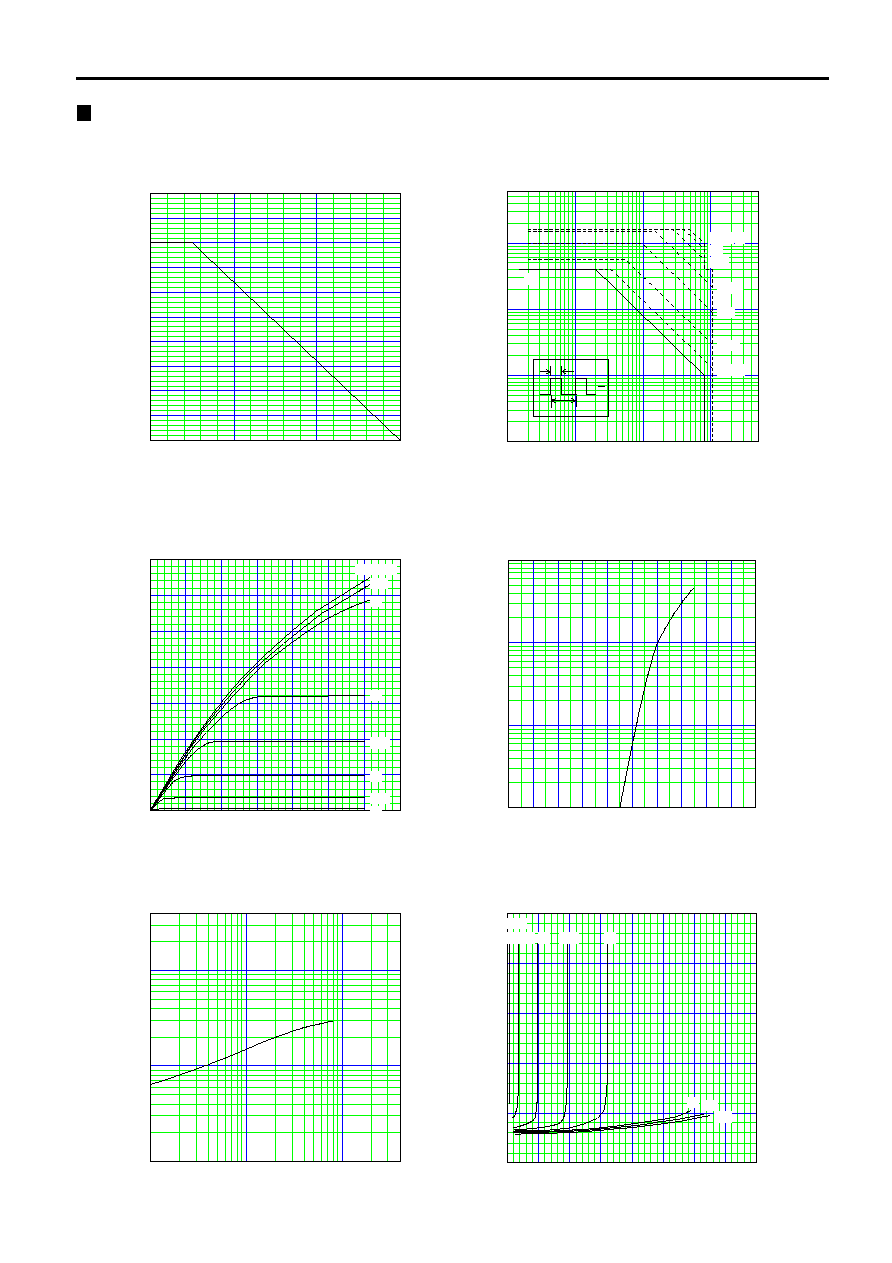
Power Dissipation
PD=f(Tc)
PD [W]
Tc [
o
C]
10
0
10
1
10
2
10
3
10
-2
10
-1
10
0
10
1
t=0.01
µ
s
Safe operating area
DC
100ms
10ms
1ms
100
µ
s
VDS [V]
ID [A]
1
µ
s
10
µ
s
t
T
D=
t
T
0
5
10
15
20
25
30
35
0
1
2
3
4
5
6
7
5V
5.5V
7V
6.5V
6V
8V
10V
VGS=20V
VDS [V]
ID [A]
Typical output characteristics
0
1
2
3
4
5
6
7
8
9
10
10
-2
10
-1
10
0
10
1
Typical transfer characteristic
ID [A]
VGS [V]
10
-1
10
0
10
1
10
-1
10
0
10
1
Typical forward transconductance
gfs [s]
ID [A]
0
1
2
3
4
5
6
7
8
0
5
10
15
20
25
8V
20V
10V
ID [A]
RDS(on) [
]
Typical drain-source on-state resistance
VGS=
7V
6.5V
5.5V 6V
5V
ID=f(VDS):D=0.01,Tc=25∞C
ID=f(VDS):80µs Pulse test,Tch=25∞C
ID=f(VGS):80µs Pulse test,VDS=25V,Tch=25∞C
gfs=f(ID):80µs Pulse test,VDS=25V,Tch=25∞C
RDS(on)=f(ID):80µs Pulse test, Tch=25∞C
3
2SK2762-01L,S
FUJI POWER MOSFET
-50
0
50
100
150
0
2
4
6
8
10
12
max.
typ.
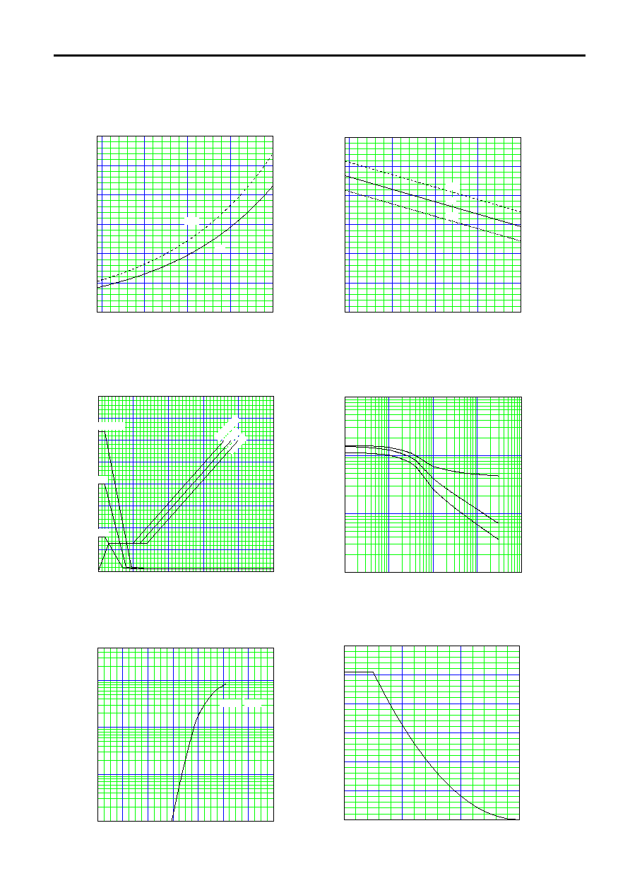
Drain-source on-state resistance
RDS(on)=f(Tch):ID=2A,VGS=10V
RDS(on) [
]
Tch [
o
C]
-50
0
50
100
150
0.0
1.0
2.0
3.0
4.0
5.0
6.0
min.
typ.
max.
Gate threshold voltage
VGS(th)=f(Tch):ID=1mA,VDS=VGS
VGS(th) [V]
Tch [
o
C]
0
20
40
60
80
100
0
100
200
300
400
500
600
700
800
Vcc=160V
400V
640V
160V
400V
Vcc=640V
VGS [V]
VDS [V]
Typical gate charge characteristic
Qg [nC]
0
5
10
15
20
25
30
35
40
10
-2
10
-1
10
0
10
1
10
2
10p
100p
1n
10n
Crss
Coss
Ciss
Typical capacitances
C=f(VDS):VGS=0V,f=1MHz
C [F]
VDS [V]
0.0
0.2
0.4
0.6
0.8
1.0
1.2
1.4
10
-2
10
-1
10
0
10
1
Tch=25
o
C typ.
Forward characteristic of reverse of diode
IF [A]
VSD [V]
0
50
100
150
0
50
100
150
200
250
300
Avalanche energy derating
Eas [mJ]
Starting Tch [
o
C]
IF=f(VSD):80µs Pulse test,VGS=0V
Eas=f(starting Tch):Vcc=80V,I
AV
=4A
VGS=f(Qg):ID=4A,Tch=25∞C
4
2SK2762-01L,S
FUJI POWER MOSFET
10
-5
10
-4
10
-3
10
-2
10
-1
10
0
10
1
10
-2
10
-1
10
0
10
1
D=0.5
0.2
0.02
0.05
0.1
0.01
0
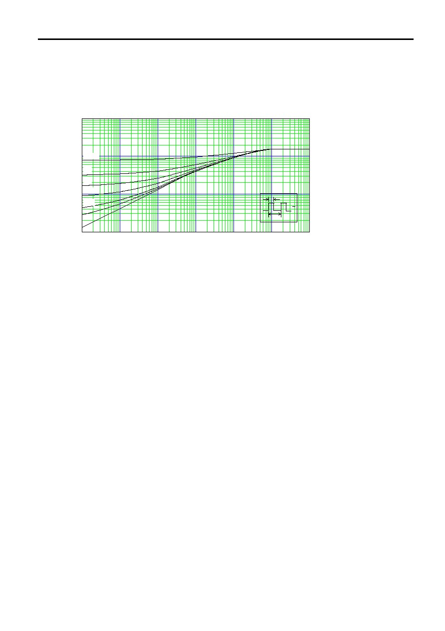
Transient thermal impedance
Zthch=f(t) parameter:D=t/T
Zthch-c [K/W]
t [s]
t
T
D=
t
T