 | –≠–ª–µ–∫—Ç—Ä–æ–Ω–Ω—ã–π –∫–æ–º–ø–æ–Ω–µ–Ω—Ç: 2SK2903 | –°–∫–∞—á–∞—Ç—å:  PDF PDF  ZIP ZIP |

1
Item
Symbol
Rating
Unit
Drain-source voltage
V
DS
60
Continuous drain current
I
D
±50
Pulsed drain current
I
D(puls]
±200
Gate-source voltage
V
GS
±30
Maximum Avalanche Energy
E
AV *1
720.8
Max. power dissipation
P
D
50
Operating and storage
T
ch
+150
temperature range
T
stg
Electrical characteristics (T
c
=25∞C unless otherwise specified)
Thermalcharacteristics
2SK2903-01MR
FUJI POWER MOS-FET
N-CHANNEL SILICON POWER MOS-FET
Features
High speed switching
Low on-resistance
No secondary breadown
Low driving power
Avalanche-proof
Applications
Switching regulators
UPS (Uninterruptible Power Supply)
DC-DC converters
Equivalent circuit schematic
Maximum ratings and characteristic
Absolute maximum ratings
(Tc=25∞C unless otherwise specified)
Gate(G)
Source(S)
Drain(D)
Item
Symbol Test Conditions
Zero gate voltage drain current I
DSS
V
DS
=60V
V
GS
=±30V
I
D
=40A V
GS
=10V
I
D
=40A V
DS
=25V
V
CC
=30V I
D
=80A
V
GS
=10V
R
GS
=10
Min. Typ. Max. Units
V
V
µA
mA
nA
m
S
pF
A
V
ns
µC
ns
Min. Typ. Max. Units
Thermal resistance
R
th(ch-c)
channel to case
R
th(ch-a)
channel to ambient
2.5
62.5
∞C/W
∞C/W
Symbol
BV
DSS
V
GS(th)
I
GSS
R
DS(on)
g
fs
C
iss
C
oss
C
rss
td
(on)
t
r
td
(off)
t
f
I
AV
V
SD
t
rr
Q
rr
Item
Drain-source breakdown voltaget
Gate threshold voltage
Gate-source leakage current
Drain-source on-state resistance
Forward transcondutance
Input capacitance
Output capacitance
Reverse transfer capacitance
Turn-on time t
on
Turn-off time t
off
Avalanche capability
Diode forward on-voltage
Reverse recovery time
Reverse recovery charge
Test Conditions
I
D
=1mA V
GS
=0V
I
D
=10mA V
DS
=V
GS
T
ch
=25∞C
V
GS
=0V T
ch
=125∞C
V
DS
=0V
V
DS
=25V
V
GS
=0V
f=1MHz
L=100 µH T
ch
=25∞C
I
F
=50A V
GS
=0V T
ch
=25∞C
I
F
=50A V
GS
=0V
-di/dt=100A/µs T
ch
=25∞C
V
A
A
V
mJ
W
∞C
∞C
*1 L=0.384mH, Vcc=24V
60
2.5
3.0
3.5
10
500
0.2
1.0
10
100
9.5
12
20
40
3100
4650
1300
1950
350
530
20
30
85
120
88
130
65
120
50
1.0
1.5
70
0.13
-55 to +150
TO-220F15
3. Source
2.54
2
Characteristics
2SK2903-01MR
FUJI POWER MOSFET
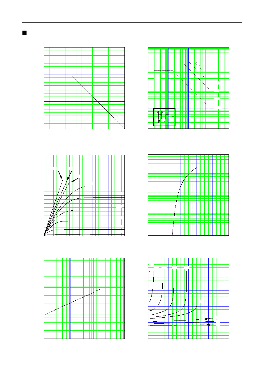
0
50
100
150
0
10
20
30
40
50
60
Power Dissipation
PD=f(Tc)
PD [W]
Tc [∞C]
10
-1
10
0
10
1
10
2
10
3
10
-1
10
0
10
1
10
2
10
3
ID [A]
VDS [V]
Safe operating area
ID=f(VDS):D=0.01,Tc=25∞C
t=
1µs
10µs
1ms
10ms
100ms
100µs
D.C.
t
T
D=
t
T
0
1
2
3
4
5
0
50
100
150
200
6.0V
5.5V
4.0V
3.5V
4.5V
10V
8V
5.0V
VGS=20V
Typical output characteristics
ID=f(VDS):80µs pulse test,Tc=25∞C
ID [A]
VDS [V]
0
2
4
6
8
10
0.1
1
10
100
Typical transfer characteristics
ID=f(VGS):80µs pulse test,VDS=25V,Tch=25∞C
ID [A]
VGS [V]
10
0
10
1
10
2
10
3
10
0
10
1
10
2
10
3
Typical forward transconductance
gfs=f(ID):80µs pulse test,VDS=25V,Tch=25∞C
gfs [s]
ID [A]
0
50
100
150
200
0
10
20
30
40
50
6V
RDS(on) [m
]
ID [A]
Typical Drain-Source on-State Resistance
RDS(on)=f(ID):80µs pulse test,Tch=25∞C
8V
10V
20V
4.5V
5.0V
4.0V
VGS=
3.5V
5.5V

3
0
20
40
60
80
100
120
140
0
5
10
15
20
25
12V
30V
Vcc=48V
Typical Gate Charge Characteristics
VGS=f(Qg):ID=80A,Tch=25∞C
0
10
20
30
40
50
VDS [V]
VGS [V]
Qg [nC]
VGS
VDS
10
-1
10
0
10
1
10
2
10
1
10
2
10
3
10
4
t [ns]
ID [A]
td(off)
tf
tr
td(on)
Typical Switching Characteristics vs. ID
t=f(ID):Vcc=30V,VGS=10V,RG=10
2SK2903-01MR
FUJI POWER MOSFET
-50
0
50
100
150
0
5
10
15
20
25
30
max.
typ.
Drain-source on-state resistance
RDS(on)=f(Tch):ID=40A,VGS=10V
RDS(on)[m
]
Tch [∞C]
-50
-25
0
25
50
75
100
125
150
0.0
0.5
1.0
1.5
2.0
2.5
3.0
3.5
4.0
4.5
5.0
VGS(th) [V]
Tch [∞C]
Gate Threshold Voltage vs. Tch
VGS(th)=f(Tch):VDS=VGS,ID=10mA
min.
typ.
max.
10
-2
10
-1
10
0
10
1
10
2
100p
1n
10n
100n
Typical capacitances
C=f(VDS):VGS=0V,f=1MHz
C [F]
VDS [V]
Ciss
Coss
Crss
0.0
0.2
0.4
0.6
0.8
1.0
1.2
1.4
1.6
20
40
60
80
100
120
140
160
180
200
Typical Forward Characteristics of Reverse Diode
IF=f(VSD):80µs pulse test,Tch=25∞C
10V
5V
VGS=0V
IF [A]
VSD [V]
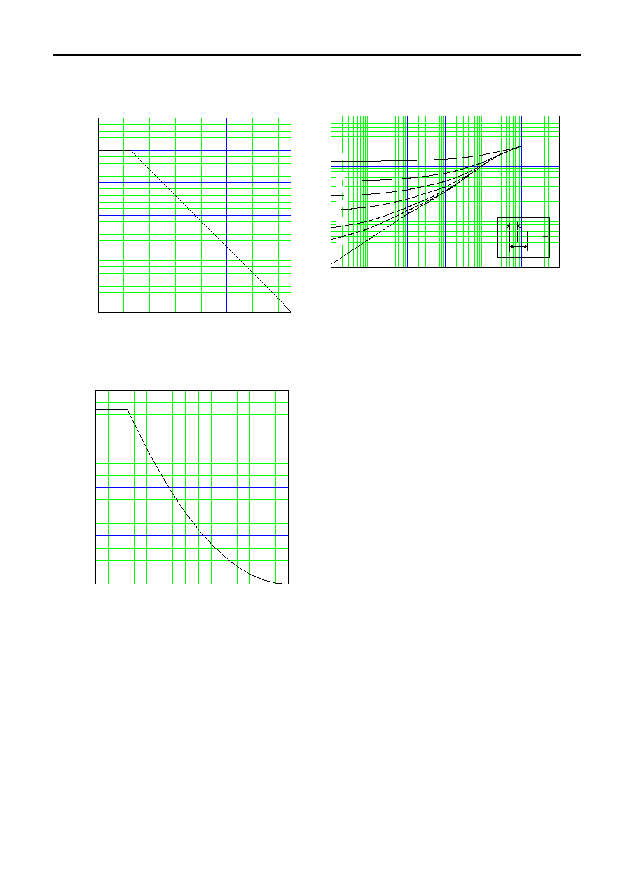
4
2SK2903-01MR
FUJI POWER MOSFET
0
50
100
150
0
10
20
30
40
50
60
Maximum Avalanche Current vs. starting Tch
I(AV)=f(starting Tch)
I(AV) [A]
Starting Tch [∞C]
0
50
100
150
0
200
400
600
800
Maximum Avalanche energy vs. starting Tch
Eas=f(starting Tch):Vcc=24V, I(AV)<=50A
Eas [mJ]
Starting Tch [∞C]
10
-5
10
-4
10
-3
10
-2
10
-1
10
0
10
1
10
-2
10
-1
10
0
10
1
0.5
0.2
0.02
0.05
0.1
0.01
0
Transient thermal impedande
Zthch=f(t) parameter:D=t/T
Zthch-c [K/W]
t [s]
t
T
D=
t
T