DATE
NAME
DRAWN
CHECKED
APPROVED
DWG.NO.
Fuji Electric Co.,Ltd.
This material and the information herein is the property of
Fuji Electric Co.,Ltd. They shall be neither reproduced, copied,
lent, or disclosed in any way whatsoever for the use of any
third party nor used for the manufacturing purposes without
the express written consent of Fuji Electric Co.,Ltd.
SPECIFICATION
Device Name : .
Type Name : .
Spec. No. : .
Fuji Electric Co.,Ltd.
Matsumoto Factory
H04-004-07
Power MOSFET
2SK3362-01
1/13
Feb.-4-'99
DWG.NO.
This material and the information herein is the property of
Fuji Electric Co.,Ltd. They shall be neither reproduced, copied,
lent, or disclosed in any way whatsoever for the use of any
third party nor used for the manufacturing purposes without
the express written consent of Fuji Electric Co.,Ltd.
H04-004-06
Fuji Electric Co.,Ltd.
2/13
1.Scope
This specifies Fuji Power MOSFET 2SK3362-01
2.Construction
N-Channel enhancement mode power MOSFET
3.Applications
for Switching
4.Outview
TO-220
Outview See to 5/13 page
5.Absolute Maximum Ratings at Tc=25
(unless otherwise specified)
Description
Symbol
Characteristics
Unit
Remarks
Drain-Source Voltage
V
DS
60
V
Continuous Drain Current
I
D
�50
A
Pulsed Drain Current
I
DP
�200
A
Gate-Source Voltage
V
GS
�
20
V
Maximum Avalanche Energy
E
AV
867
mJ
*1
Maximum Power Dissipation
P
D
80
W
Operating and Storage
T
ch
150
Temperature range
T
stg
-55 to +150
*1 L=0.463mH,Vcc=24V
6.Electrical Characteristics at Tc=25
(unless otherwise specified)
Static Ratings
Description
Symbol
Conditions
min.
typ.
max.
Unit
Drain-Source
I
D
=1mA
Breakdown Voltage
V
GS
=0V
60
V
Gate Threshold
I
D
=1mA
Voltage
V
DS
=V
GS
1.0
1.5
2.0
V
Zero Gate Voltage
V
DS
=60V
T
ch
=25
10
500
A
Drain Current
V
GS
=0V
T
ch
=125
0.2
1.0
mA
Gate-Source
V
GS
=
�
20V
Leakage Current
V
DS
=0V
10
100
nA
Drain-Source
VGS=4V
12
17
On-State Resistance
VGS=10V
7.5
10
m
ID=40A
BV
DSS
V
GS
(th)
I
DSS
I
GSS
R
DS
(on)

DWG.NO.
This material and the information herein is the property of
Fuji Electric Co.,Ltd. They shall be neither reproduced, copied,
lent, or disclosed in any way whatsoever for the use of any
third party nor used for the manufacturing purposes without
the express written consent of Fuji Electric Co.,Ltd.
H04-004-03
Fuji Electric Co.,Ltd.
MS5F4388
3/13
Dynamic Ratings
Description
Symbol
Conditions
min.
typ.
max.
Unit
Forward
I
D
=40A
Transconductance
V
DS
=25V
25.0
55.0
S
Input Capacitance
Ciss
V
DS
=25V
3500
5250
Output Capacitance
Coss
V
GS
=0V
1250
1870
Reverse Transfer
f=1MHz
pF
Capacitance
360
540
td(on)
V
cc
=30V
15
23
Turn-On Time
tr
V
GS
=10V
75
120
td(off)
I
D
=75A
190
285
ns
Turn-Off Time
tf
R
GS
=10
110
165
Reverse Diode
Description
Symbol
Conditions
min.
typ.
max.
Unit
Avalanche Capability
L=100
H
Tch=25
See Fig.1 and Fig.2
50
A
Diode Forward
I
F
=160A
On-Voltage
V
GS
=0V
T
ch
=25
1.15
1.65
V
Reverse Recovery
I
F
=80A
Time
V
GS
=0V
75
120
ns
Reverse Recovery
-di/dt=100A/
s
Charge
T
ch
=25
0.17
C
7.Thermal Resistance
Description
Symbol
min.
typ.
max.
Unit
Channel to Case
Rth(ch-c)
1.56
/W
Channel to Ambient
Rth(ch-a)
75.0
/W
trr
Qrr
g
fs
Crss
I
AV
V
SD

DWG.NO.
This material and the information herein is the property of
Fuji Electric Co.,Ltd. They shall be neither reproduced, copied,
lent, or disclosed in any way whatsoever for the use of any
third party nor used for the manufacturing purposes without
the express written consent of Fuji Electric Co.,Ltd.
H04-004-03
Fuji Electric Co.,Ltd.
MS5F4388
4/13
Fig.2 Operating waveforms
0
0
BV
DSS
I
AV
V
GS
I
D
V
DS
Fig.1 Test circuit
50
D.U.T
L
Vcc
Vcc=24V
L=100uH
Starting Tch=25
1 shot pulse
10V

DWG.NO.
This material and the information herein is the property of
Fuji Electric Co.,Ltd. They shall be neither reproduced, copied,
lent, or disclosed in any way whatsoever for the use of any
third party nor used for the manufacturing purposes without
the express written consent of Fuji Electric Co.,Ltd.
H04-004-03
Fuji Electric Co.,Ltd.
MS5F4388
5/13

DWG.NO.
This material and the information herein is the property of
Fuji Electric Co.,Ltd. They shall be neither reproduced, copied,
lent, or disclosed in any way whatsoever for the use of any
third party nor used for the manufacturing purposes without
the express written consent of Fuji Electric Co.,Ltd.
H04-004-03
Fuji Electric Co.,Ltd.
MS5F4388
6/13
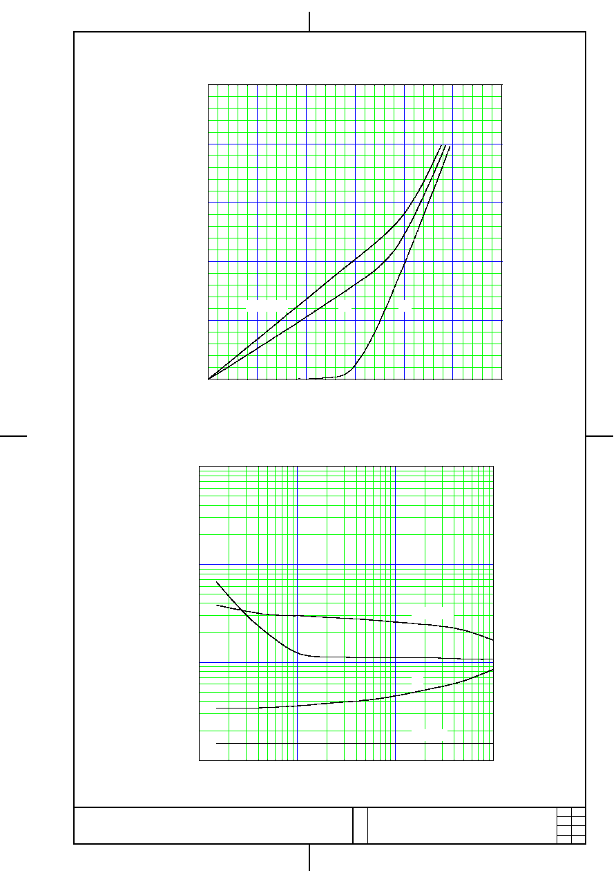
10
0
10
1
10
2
10
0
10
1
10
2
ID [A]
VDS [V]
Safe operating area
ID=f(VDS):D=0.01,Tc=25
t=
1us
10
�
s
1ms
10ms
100ms
100
�
s
D.C.
0
25
50
75
100
125
150
0
20
40
60
80
100
Power Dissipation
PD=f(Tc)
PD [W]
Tc []
T
T
t
t
D=

DWG.NO.
This material and the information herein is the property of
Fuji Electric Co.,Ltd. They shall be neither reproduced, copied,
lent, or disclosed in any way whatsoever for the use of any
third party nor used for the manufacturing purposes without
the express written consent of Fuji Electric Co.,Ltd.
H04-004-03
Fuji Electric Co.,Ltd.
MS5F4388
7/13
0.0
0.5
1.0
1.5
2.0
2.5
0
20
40
60
80
100
120
140
160
ID
[
A
]
V D S [V ]
Typical Output C haracteris tics
ID=f(VDS ):80
�
s pulse test,Tch= 25
10 V
15 V
20 V
8 V
6 V
5.0 V
4.5 V
4.0 V
3.5 V
3.0 V
V G S = 2.5 V
0
1
2
3
4
5
0
20
40
60
80
100
ID
[A]
VG S [ V ]
Typical Transfer Characte ri stic
ID=f(V GS ):80
�
s puls e test,VD S=25V,Tc h= 25

DWG.NO.
This material and the information herein is the property of
Fuji Electric Co.,Ltd. They shall be neither reproduced, copied,
lent, or disclosed in any way whatsoever for the use of any
third party nor used for the manufacturing purposes without
the express written consent of Fuji Electric Co.,Ltd.
H04-004-03
Fuji Electric Co.,Ltd.
MS5F4388
8/13
10
- 1
10
0
10
1
10
2
10
- 1
10
0
10
1
10
2
gf
s
[S]
ID [ A ]
Ty pical T ransco nductanc e
gf s=f(ID): 80
�
s puls e test, VDS=25 V,Tch=25
0
20
40
60
80
100
120
140
160
180
0
5
10
15
20
25
30
35
R
DS(o
n)
[m
]
ID [ A ]
Ty pical Drain-S ource on -State Resista nce
RDS(on )=f(ID) :80
�
s pu lse tes t,Tch=2 5
1 0 V
1 5 V
2 0 V
8 V
6 V
5. 0 V
4. 5 V
4. 0 V
3. 5 V
3. 0 V

DWG.NO.
This material and the information herein is the property of
Fuji Electric Co.,Ltd. They shall be neither reproduced, copied,
lent, or disclosed in any way whatsoever for the use of any
third party nor used for the manufacturing purposes without
the express written consent of Fuji Electric Co.,Ltd.
H04-004-03
Fuji Electric Co.,Ltd.
MS5F4388
9/13
- 50
0
50
100
150
0
5
10
15
20
R
DS(on)
[
m
]
T c h []
typ .
max .
D rain-Sou rc e On-sta te Resista nce
RDS(o n) =f(Tch): ID =25A,VGS =10V
-50
-25
0
25
50
75
100
125
150
0.0
0.5
1.0
1.5
2.0
2.5
3.0
VG
S(t
h) [
m
V
]
Tc h [ ]
Gate Thres hold Voltage vs. Tch
VGS(th)=f (Tch):VDS=VGS ,ID=1mA
m in .
t yp .
m ax .

DWG.NO.
This material and the information herein is the property of
Fuji Electric Co.,Ltd. They shall be neither reproduced, copied,
lent, or disclosed in any way whatsoever for the use of any
third party nor used for the manufacturing purposes without
the express written consent of Fuji Electric Co.,Ltd.
H04-004-03
Fuji Electric Co.,Ltd.
MS5F4388
10/13
10
-2
10
-1
10
0
10
1
10
2
10
- 11
10
- 10
10
-9
10
-8
10
-7
C [
F]
V DS [V ]
T yp ical C apacita nce
C=f( VD S):VGS =0V,f=1 MHz
C rs s
C os s
C is s
0
50
100
150
200
250
0
5
10
15
20
25
12V
30V
Vc c=48V
T ypical Gate Cha rge Cha racteris tics
VGS=f( Qg):ID= 80A,Tch= 25
0
10
20
30
40
50
VD
S
[
V
]
VG
S
[
V
]
Qg [ nC ]
V G S
V D S
DWG.NO.
This material and the information herein is the property of
Fuji Electric Co.,Ltd. They shall be neither reproduced, copied,
lent, or disclosed in any way whatsoever for the use of any
third party nor used for the manufacturing purposes without
the express written consent of Fuji Electric Co.,Ltd.
H04-004-03
Fuji Electric Co.,Ltd.
MS5F4388
11/13
10
-1
10
0
10
1
10
2
10
1
10
2
10
3
10
4
t
[n
s]
I D [A ]
t d ( o ff )
t f
t r
t d ( on )
Typical Sw itc hing Characteri st ics vs. ID
t =f( ID):Vcc=30V,VGS =1 0V,RG=10
0.00
0.25
0.50
0.75
1.00
1.25
1.50
0
50
100
150
200
250
I
F
[A]
VSD [ V ]
0 V
5 V
VGS = 1 0 V
Typical F orward Char ac teristics o f Reverse Di ode
IF=f(VSD) :80
�
s pu ls e test,Tch=2 5

DWG.NO.
This material and the information herein is the property of
Fuji Electric Co.,Ltd. They shall be neither reproduced, copied,
lent, or disclosed in any way whatsoever for the use of any
third party nor used for the manufacturing purposes without
the express written consent of Fuji Electric Co.,Ltd.
H04-004-03
Fuji Electric Co.,Ltd.
MS5F4388
12/13
0
25
50
75
100
125
150
0
10
20
30
40
50
60
E
(AV) [mJ]
I
(AV) [A]
Maximum Avalanche Current vs. starting Tch
I(AV)=f(starting Tch)
0
25
50
75
100
125
150
0
200
400
600
800
1000
starting Tch []
starting Tch []
Maximum Avalanche Energy vs. starting Tch
E(AV)=f(starting Tch):Vcc=24V,I(AV)50A

DWG.NO.
This material and the information herein is the property of
Fuji Electric Co.,Ltd. They shall be neither reproduced, copied,
lent, or disclosed in any way whatsoever for the use of any
third party nor used for the manufacturing purposes without
the express written consent of Fuji Electric Co.,Ltd.
H04-004-03
Fuji Electric Co.,Ltd.
MS5F4388
13/13
10
-5
10
-4
10
-3
10
-2
10
-1
10
0
10
1
10
-2
10
-1
10
0
10
1
D=0.5
0.2
0.02
0.05
0.1
0.01
0
Transient thermal impedance
Zthch=f(t) parameter:D=t/T
Zthch-c [K/W]
t [s]
T
T
t
t
D=