 | –≠–ª–µ–∫—Ç—Ä–æ–Ω–Ω—ã–π –∫–æ–º–ø–æ–Ω–µ–Ω—Ç: 2SK3521 | –°–∫–∞—á–∞—Ç—å:  PDF PDF  ZIP ZIP |
1
P4
Item
Symbol
Ratings
Unit
Drain-source voltage
V
DS
500
Continuous drain current
I
D
±8
Pulsed drain current
I
D(puls]
±32
Gate-source voltage
V
GS
±30
Repetitive or non-repetitive
I
AR *2
8
Maximum Avalanche Energy
E
AS *1
173
Maximum Drain-Source dV/dt
dV
DS
/dt
*4
20
Peak Diode Recovery dV/dt
dV/dt
*3
5
Max. power dissipation
P
D
Ta=25∞C
1.67
Tc=25∞C
65
Operating and storage
T
ch
+150
temperature range
T
stg
Electrical characteristics (T
c
=25∞C unless otherwise specified)
Thermalcharacteristics
2SK3521-01L,S,SJ
FUJI POWER MOSFET
N-CHANNEL SILICON POWER MOSFET
Features
High speed switching
Low on-resistance
No secondary breadown
Low driving power
Avalanche-proof
Applications
Switching regulators
UPS (Uninterruptible Power Supply)
DC-DC converters
Maximum ratings and characteristic
Absolute maximum ratings
(Tc=25∞C unless otherwise specified)
Item
Symbol Test Conditions
Zero gate voltage drain current I
DSS
V
DS
=500V V
GS
=0V
V
DS
=400V V
GS
=0V
V
GS
=±30V
I
D
=4A V
GS
=10V
I
D
=4A V
DS
=25V
V
CC
=300V I
D
=4A
V
GS
=10V
R
GS
=10
Min. Typ. Max. Units
V
V
µA
nA
S
pF
nC
A
V
µs
µC
ns
Min. Typ. Max. Units
Thermal resistance
R
th(ch-c)
channel to case
R
th(ch-a)
channel to ambient
1.92
75.0
∞C/W
∞C/W
Symbol
V
(BR)DSS
V
GS(th)
I
GSS
R
DS(on)
g
fs
C
iss
C
oss
C
rss
td
(on)
t
r
td
(off)
t
f
Q
G
Q
GS
Q
GD
I
AV
V
SD
t
rr
Q
rr
Item
Drain-source breakdown voltaget
Gate threshold voltage
Gate-source leakage current
Drain-source on-state resistance
Forward transcondutance
Input capacitance
Output capacitance
Reverse transfer capacitance
Turn-on time t
on
Turn-off time t
off
Total Gate Charge
Gate-Source Charge
Gate-Drain Charge
Avalanche capability
Diode forward on-voltage
Reverse recovery time
Reverse recovery charge
Test Conditions
I
D
= 250µA V
GS
=0V
I
D
= 250µA V
DS
=V
GS
T
ch
=25∞C
T
ch
=125∞C
V
DS
=0V
V
DS
=25V
V
GS
=0V
f=1MHz
V
CC
=250V
I
D
=8A
V
GS
=10V
L=4.98mH T
ch
=25∞C
I
F
=8A V
GS
=0V T
ch
=25∞C
I
F
=8A V
GS
=0V
-di/dt=100A/µs T
ch
=25∞C
V
A
A
V
A
mJ
kV/µs
kV/µs
W
∞C
∞C
500
3.0
5.0
25
250
10
100
0.65
0.85
3.5
7
750
1130
100
150
4.0
6.0
14
21
9
14
24
36
6
9
20
30
8.5
13
5.5
8.5
8
1.00
1.50
0.65
3.5
-55 to +150
Outline Drawings
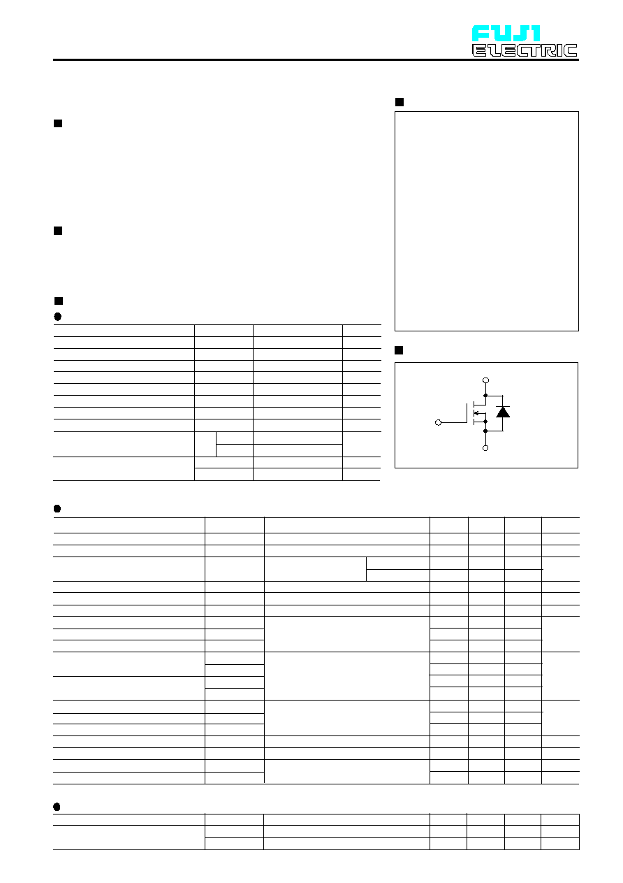
Equivalent circuit schematic
Gate(G)
Source(S)
Drain(D)
Super FAP-G Series
*3 I
F
-I
D
, -di/dt=50A/µs, Vcc BV
DSS
, Tch 150∞C
=
<
=
<
=
<
*1 L=4.98mH, Vcc=50V *2 Tch 150∞C
=
<
*4 VDS 500V
<=
2
0
2
4
6
8 10 12 14 16 18 20 22 24 26 28 30
0
2
4
6
8
10
12
14
16
18
20
20V
10V
8V
7.5V
7.0V
ID [A]
VDS [V]
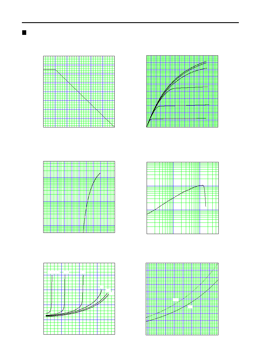
Typical Output Characteristics
VGS=6.5V
Characteristics
2SK3521-01L,S,SJ
FUJI POWER MOSFET
ID=f(VGS):80µs Pulse test, VDS=25V,Tch=25∞C
ID=f(VDS):80µs Pulse test,Tch=25∞C
gfs=f(ID):80µs Pulse test, VDS=25V,Tch=25∞C
RDS(on)=f(ID):80µs Pulse test, Tch=25∞C
0
1
2
3
4
5
6
7
8
9
10
0.1
1
10
ID[A]
VGS[V]
Typical Transfer Characteristic
0.1
1
10
0.1
1
10
100
gfs [S]
ID [A]
Typical Transconductance
0
5
10
15
20
0.0
0.5
1.0
1.5
2.0
RDS(on) [
]
ID [A]
Typical Drain-Source on-state Resistance
10V
20V
8V
7.5V
7.0V
VGS=6.5V
-50
-25
0
25
50
75
100
125
150
0.0
0.2
0.4
0.6
0.8
1.0
1.2
1.4
1.6
1.8
2.0
RDS(on) [
]
Tch [
∞
C]
typ.
max.
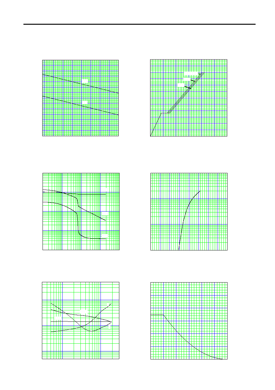
Drain-Source On-state Resistance
RDS(on)=f(Tch):ID=4A,VGS=10V
0
25
50
75
100
125
150
0
10
20
30
40
50
60
70
80
Allowable Power Dissipation
PD=f(Tc)
P
D
[W
]
Tc [
∞
C]
3
0.00
0.25
0.50
0.75
1.00
1.25
1.50
1.75
2.00
0.1
1
10
100
IF [A]
VSD [V]
Typical Forward Characteristics of Reverse Diode
2SK3521-01S,L,SJ
FUJI POWER MOSFET
VGS=f(Qg):ID=8A, Tch=25∞C
IF=f(VSD):80µs Pulse test,Tch=25∞C
t=f(ID):Vcc=300V, VGS=10V, RG=10
0
10
20
30
40
50
60
0
2
4
6
8
10
12
14
16
18
20
22
24
Qg [nC]
Typical Gate Charge Characteristics
VGS [V]
400V
250V
Vcc= 100V
10
-1
10
0
10
1
10
2
10
3
1p
10p
100p
1n
10n
C [F]
VDS [V]
Typical Capacitance
C=f(VDS):VGS=0V,f=1MHz
Crss
Coss
Ciss
10
0
10
1
10
0
10
1
10
2
Typical Switching Characteristics vs. ID
td(on)
tr
tf
td(off)
t [ns]
ID [A]
0
25
50
75
100
125
150
0
50
100
150
200
250
300
EAV [mJ]
starting Tch [
∞
C]
Maximum Avalanche Energy vs. starting Tch
E(AV)=f(starting Tch):Vcc=50V,I(AV)<=8A
-50
-25
0
25
50
75
100
125
150
0.0
0.5
1.0
1.5
2.0
2.5
3.0
3.5
4.0
4.5
5.0
5.5
6.0
6.5
7.0
max.
min.
Gate Threshold Voltage vs. Tch
VGS(th)=f(Tch):VDS=VGS,ID=250uA
VGS(
t
h
)
[V]
Tch [
∞
C]
4
2SK3521-01L,S,SJ
FUJI POWER MOSFET
I
AV
=f(t
AV
):starting Tch=25∞C. Vcc=50V
A
valanche current I
AV
[A]
10
-8
10
-7
10
-6
10
-5
10
-4
10
-3
10
-2
10
-2
10
-1
10
0
10
1
10
2
Single Pulse
Maximum Avalanche Current Pulsewidth
t
AV
[sec]
PRE-SOLDER
See Note: 1.
Trademark
Lot No.
Type name
Note: 1. Guaranteed mark of avalanche ruggedness.
CONNECTION
GATE
DRAIN
SOURCE
DIMENSIONS ARE IN MILLIMETERS.
FUJI POWER MOS FET
1
2
3
1
2
3
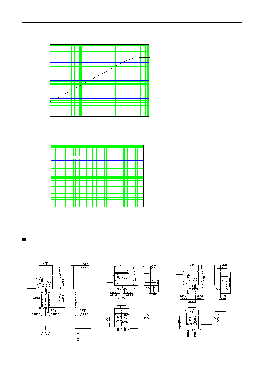
Outline Drawings (mm)
Type(L)
GATE
DRAIN
SOURCE
See Note: 1.
Trademark
Lot No.
DIMENSIONS ARE IN MILLIMETERS.
Type name
FUJI POWER MOS FET
CONNECTION
Notes
1. ( ) : Reference dimensions.
Note: 1. Guaranteed mark of
avalanche ruggedness.
2. The metal part is covered with
the solder plating, part of cutting
is without the solder plating.
Pre-Solder
Fig. 1.
Fig. 1.
OUT VIEW
Solder Plating
4
1
2
4
3
Type(S)
GATE
DRAIN
SOURCE
See Note: 1.
Trademark
Lot No.
Type name
FUJI POWER MOS FET
CONNECTION
Notes
1. ( ) : Reference dimensions.
Note: 1. Guaranteed mark of
avalanche ruggedness.
2. The metal part is covered with
the solder plating, part of cutting
is without the solder plating.
OUT VIEW
Fig. 1.
Fig. 1.
Solder Plating
Pre-Solder
DIMENSIONS ARE IN MILLIMETERS.
2
4
1
3
Type(SJ)
10
-6
10
-5
10
-4
10
-3
10
-2
10
-1
10
0
10
-3
10
-2
10
-1
10
0
10
1
Transient Thermal Impedance
Zth(ch-c)=f(t):D=0
Z
t
h
(
ch-
c)
[
/
W
]
t [sec]