 | –≠–ª–µ–∫—Ç—Ä–æ–Ω–Ω—ã–π –∫–æ–º–ø–æ–Ω–µ–Ω—Ç: 2SK3522 | –°–∫–∞—á–∞—Ç—å:  PDF PDF  ZIP ZIP |
1
Item
Symbol
Ratings
Unit
Drain-source voltage
V
DS
500
V
DSX *5
500
Continuous drain current
I
D
±21
Pulsed drain current
I
D(puls]
±84
Gate-source voltage
V
GS
±30
Repetitive or non-repetitive
I
AR *2
21
Maximum Avalanche Energy
E
AS *1
400
Maximum Drain-Source dV/dt
dV
DS
/dt
*4
20
Peak Diode Recovery dV/dt
dV/dt
*3
5
Max. power dissipation
P
D
Ta=25∞C
2.50
Tc=25∞C
220
Operating and storage
T
ch
+150
temperature range
T
stg
Electrical characteristics (T
c
=25∞C unless otherwise specified)
Thermalcharacteristics
2SK3522-01
FUJI POWER MOSFET
N-CHANNEL SILICON POWER MOSFET
Features
High speed switching
Low on-resistance
No secondary breadown
Low driving power
Avalanche-proof
Applications
Switching regulators
UPS (Uninterruptible Power Supply)
DC-DC converters
Maximum ratings and characteristic
Absolute maximum ratings
(Tc=25∞C unless otherwise specified)
Item
Symbol Test Conditions
Zero gate voltage drain current I
DSS
V
DS
=500V V
GS
=0V
V
DS
=400V V
GS
=0V
V
GS
=±30V
I
D
=10.5A V
GS
=10V
I
D
=10.5A V
DS
=25V
V
CC
=300V I
D
=10.5A
V
GS
=10V
R
GS
=10
Min. Typ. Max. Units
V
V
µA
nA
S
pF
nC
A
V
µs
µC
ns
Min. Typ. Max. Units
Thermal resistance
R
th(ch-c)
channel to case
R
th(ch-a)
channel to ambient
0.568
50.0
∞C/W
∞C/W
Symbol
V
(BR)DSS
V
GS(th)
I
GSS
R
DS(on)
g
fs
C
iss
C
oss
C
rss
td
(on)
t
r
td
(off)
t
f
Q
G
Q
GS
Q
GD
I
AV
V
SD
t
rr
Q
rr
Item
Drain-source breakdown voltaget
Gate threshold voltage
Gate-source leakage current
Drain-source on-state resistance
Forward transcondutance
Input capacitance
Output capacitance
Reverse transfer capacitance
Turn-on time t
on
Turn-off time t
off
Total Gate Charge
Gate-Source Charge
Gate-Drain Charge
Avalanche capability
Diode forward on-voltage
Reverse recovery time
Reverse recovery charge
Test Conditions
I
D
= 250µA V
GS
=0V
I
D
= 250µA V
DS
=V
GS
T
ch
=25∞C
T
ch
=125∞C
V
DS
=0V
V
DS
=25V
V
GS
=0V
f=1MHz
V
CC
=300V
I
D
=21A
V
GS
=10V
L=1.67mH T
ch
=25∞C
I
F
=21A V
GS
=0V T
ch
=25∞C
I
F
=21A V
GS
=0V
-di/dt=100A/µs T
ch
=25∞C
V
V
A
A
V
A
mJ
kV/µs
kV/µs
W
∞C
∞C
500
3.0
5.0
25
250
10
100
0.20
0.26
11
22
2280
3420
320
480
16
24
27
41
37
56
75
113
11
17
54
81
16
24
20
30
21
0.98
1.50
0.7
10.0
-55 to +150
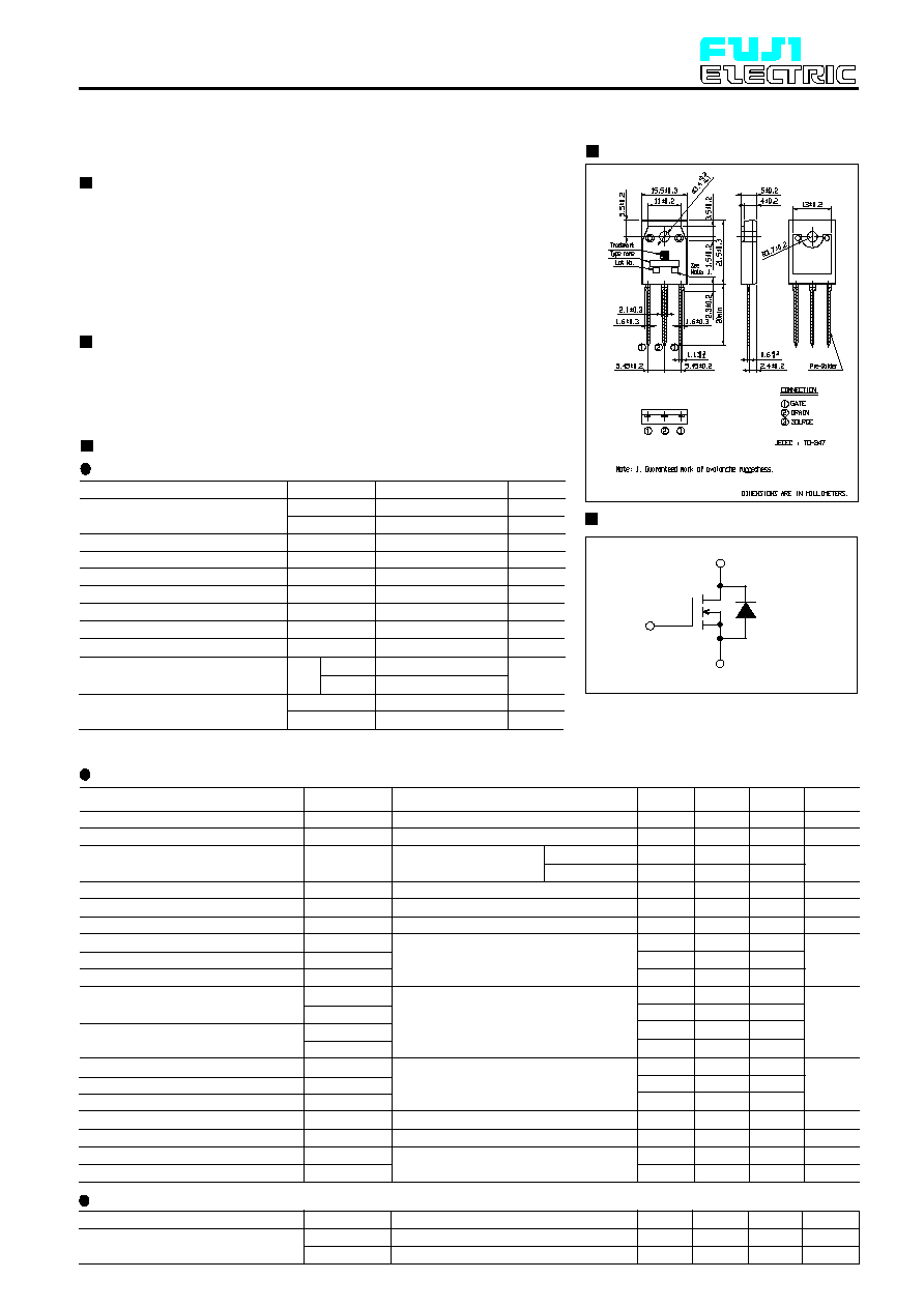
Outline Drawings
Equivalent circuit schematic
Gate(G)
Source(S)
Drain(D)
Super FAP-G Series
*3 I
F
-I
D
, -di/dt=50A/µs, Vcc BV
DSS
, Tch 150∞C
=
<
=
<
=
<
*1 L=1.67mH, Vcc=50V *2 Tch 150∞C
=
<
*4 VDS 500V *5 V
GS
=-30V
<
=

2
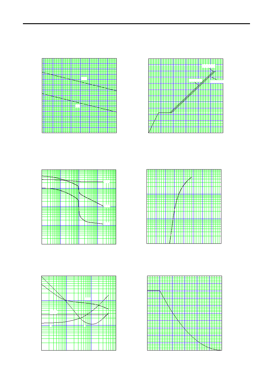
Characteristics
2SK3522-01
FUJI POWER MOSFET
ID=f(VGS):80µs Pulse test, VDS=25V,Tch=25∞C
ID=f(VDS):80µs Pulse test,Tch=25∞C
gfs=f(ID):80µs Pulse test, VDS=25V,Tch=25∞C
RDS(on)=f(ID):80µs Pulse test, Tch=25∞C
0
25
50
75
100
125
150
0
20
40
60
80
100
120
140
160
180
200
220
240
260
Allowable Power Dissipation
PD=f(Tc)
PD
[W
]
Tc [
∞
C]
0
2
4
6
8
10
12
14
16
18
20
0
5
10
15
20
25
30
35
40
45
50
55
20V
7.0V
10V
8V
6.5V
6.0V
ID
[A]
VDS [V]
Typical Output Characteristics
VGS=5.5V
0
1
2
3
4
5
6
7
8
9
10
0.1
1
10
100
ID
[A]
VGS[V]
Typical Transfer Characteristic
0.1
1
10
100
0.1
1
10
100
g
f
s [S
]
ID [A]
Typical Transconductance
0
5
10
15
20
25
30
35
40
45
50
55
0.0
0.1
0.2
0.3
0.4
0.5
0.6
7.0V
6.5V
RD
S(
on)
[
]
ID [A]
Typical Drain-Source on-state Resistance
10V
20V
8V
6.0V
VGS=
5.5V
-50
-25
0
25
50
75
100
125
150
0.0
0.1
0.2
0.3
0.4
0.5
0.6
0.7
RDS
(
o
n
)
[
]
Tch [
∞
C]
typ.
max.
Drain-Source On-state Resistance
RDS(on)=f(Tch):ID=10.5A,VGS=10V
3
2SK3522-01
FUJI POWER MOSFET
VGS=f(Qg):ID=21A, Tch=25∞C
IF=f(VSD):80µs Pulse test,Tch=25∞C
t=f(ID):Vcc=300V, VGS=10V, RG=10
VGS(th)=f(Tch):VDS=VGS,ID=250µA
-50
-25
0
25
50
75
100
125
150
0.0
0.5
1.0
1.5
2.0
2.5
3.0
3.5
4.0
4.5
5.0
5.5
6.0
6.5
7.0
max.
min.
Gate Threshold Voltage vs. Tch
VGS(
t
h
)
[
V
]
Tch [
∞
C]
0
20
40
60
80
100
120
0
2
4
6
8
10
12
14
16
18
20
22
24
Vcc= 100V
Vcc= 400V
Qg [nC]
Typical Gate Charge Characteristics
VGS [V
]
Vcc= 250V
10
-1
10
0
10
1
10
2
10
3
10
-3
10
-2
10
-1
10
0
10
1
C [
n
F
]
VDS [V]
Typical Capacitance
C=f(VDS):VGS=0V,f=1MHz
Crss
Coss
Ciss
0.00
0.25
0.50
0.75
1.00
1.25
1.50
1.75
2.00
0.1
1
10
100
IF
[A]
VSD [V]
Typical Forward Characteristics of Reverse Diode
10
-1
10
0
10
1
10
2
10
0
10
1
10
2
10
3
Typical Switching Characteristics vs. ID
td(on)
tr
tf
td(off)
t [n
s]
ID [A]
0
25
50
75
100
125
150
0
50
100
150
200
250
300
350
400
450
500
EAV
[m
J]
starting Tch [
∞
C]
Maximum Avalanche Energy vs. starting Tch
E(AV)=f(starting Tch):Vcc=50V,I(AV)<=21A

4
2SK3522-01
FUJI POWER MOSFET
I
AV
=f(t
AV
):starting Tch=25∞C. Vcc=50V
A
valanche current I
AV
[A]
10
-6
10
-5
10
-4
10
-3
10
-2
10
-1
10
0
10
-3
10
-2
10
-1
10
0
10
1
Transient Thermal Impedance
Zth(ch-c)=f(t):D=t/T,D=0
Zt
h(c
h
-c
) [
o
C/
W
]
t [sec]
10
-8
10
-7
10
-6
10
-5
10
-4
10
-3
10
-2
10
-2
10
-1
10
0
10
1
10
2
Single Pulse
Maximum Avalanche Current Pulsewidth
t
AV
[sec]