1
TO-220F
Item
Symbol
Ratings
Unit
Drain-source voltage
V
DS
100
V
DSX *5
70
Continuous drain current
I
D
±29
Pulsed drain current
I
D(puls]
±116
Gate-source voltage
V
GS
±30
Non-repetitive Avalanche current
I
AS *2
29
Maximum Avalanche Energy
E
AS *1
155.8
Maximum Drain-Source dV/dt
dV
DS
/dt
*4
20
Peak Diode Recovery dV/dt
dV/dt
*3
5
Max. power dissipation
P
D
Ta=25∞C
2.16
Tc=25∞C
37
Operating and storage
T
ch
+150
temperature range
T
stg
Isolation voltage
V
ISO *6
2
Electrical characteristics (T
c
=25∞C unless otherwise specified)
Thermalcharacteristics
2SK3599-01MR
FUJI POWER MOSFET
N-CHANNEL SILICON POWER MOSFET
Features
High speed switching
Low on-resistance
No secondary breadown
Low driving power
Avalanche-proof
Applications
Switching regulators
UPS (Uninterruptible Power Supply)
DC-DC converters
Maximum ratings and characteristic
Absolute maximum ratings
(Tc=25∞C unless otherwise specified)
Item
Symbol Test Conditions
Zero gate voltage drain current I
DSS
V
DS
=100V V
GS
=0V
V
DS
=80V V
GS
=0V
V
GS
=±30V
I
D
=10A V
GS
=10V
I
D
=10A V
DS
=25V
V
CC
=48V I
D
=10A
V
GS
=10V
R
GS
=10
Min. Typ. Max. Units
V
V
µA
nA
m
S
pF
nC
A
V
ns
µC
ns
Min. Typ. Max. Units
Thermal resistance
R
th(ch-c)
channel to case
R
th(ch-a)
channel to ambient
3.378
58.0
∞C/W
∞C/W
Symbol
V
(BR)DSS
V
GS(th)
I
GSS
R
DS(on)
g
fs
C
iss
C
oss
C
rss
td
(on)
t
r
td
(off)
t
f
Q
G
Q
GS
Q
GD
I
AV
V
SD
t
rr
Q
rr
Item
Drain-source breakdown voltaget
Gate threshold voltage
Gate-source leakage current
Drain-source on-state resistance
Forward transcondutance
Input capacitance
Output capacitance
Reverse transfer capacitance
Turn-on time t
on
Turn-off time t
off
Total Gate Charge
Gate-Source Charge
Gate-Drain Charge
Avalanche capability
Diode forward on-voltage
Reverse recovery time
Reverse recovery charge
Test Conditions
I
D
= 250µA V
GS
=0V
I
D
= 250µA V
DS
=V
GS
T
ch
=25∞C
T
ch
=125∞C
V
DS
=0V
V
DS
=75V
V
GS
=0V
f=1MHz
V
CC
=50V
I
D
=20A
V
GS
=10V
L=222µH T
ch
=25∞C
I
F
=20A V
GS
=0V T
ch
=25∞C
I
F
=20A V
GS
=0V
-di/dt=100A/µs T
ch
=25∞C
V
V
A
A
V
A
mJ
kV/µs
kV/µs
W
∞C
∞C
kVrms
100
3.0
5.0
25
250
10
100
47
62
6
12
730
1095
190
285
12
18
12
18
3.8
6
23
35
8.5
13
22
33
9
13.5
6
9
29
1.10
1.65
65
0.17
-55 to +150
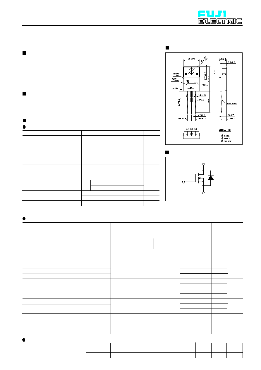
Outline Drawings
(mm)
Equivalent circuit schematic
Gate(G)
Source(S)
Drain(D)
Super FAP-G Series
*3 I
F
-I
D
, -di/dt=50A/µs, Vcc BV
DSS
, Tch 150∞C
=
<
=
<
=
<
*4 V
DS
100V
<=
www.fujielectric.co.jp/denshi/scd
*5 V
GS
=-30V *6 t=60sec f=60Hz
200304
*1 L=222µH, Vcc=48V, Tch=25∞C, See to Avalanche Energy Graph *2 Tch 150∞C
=
<

2
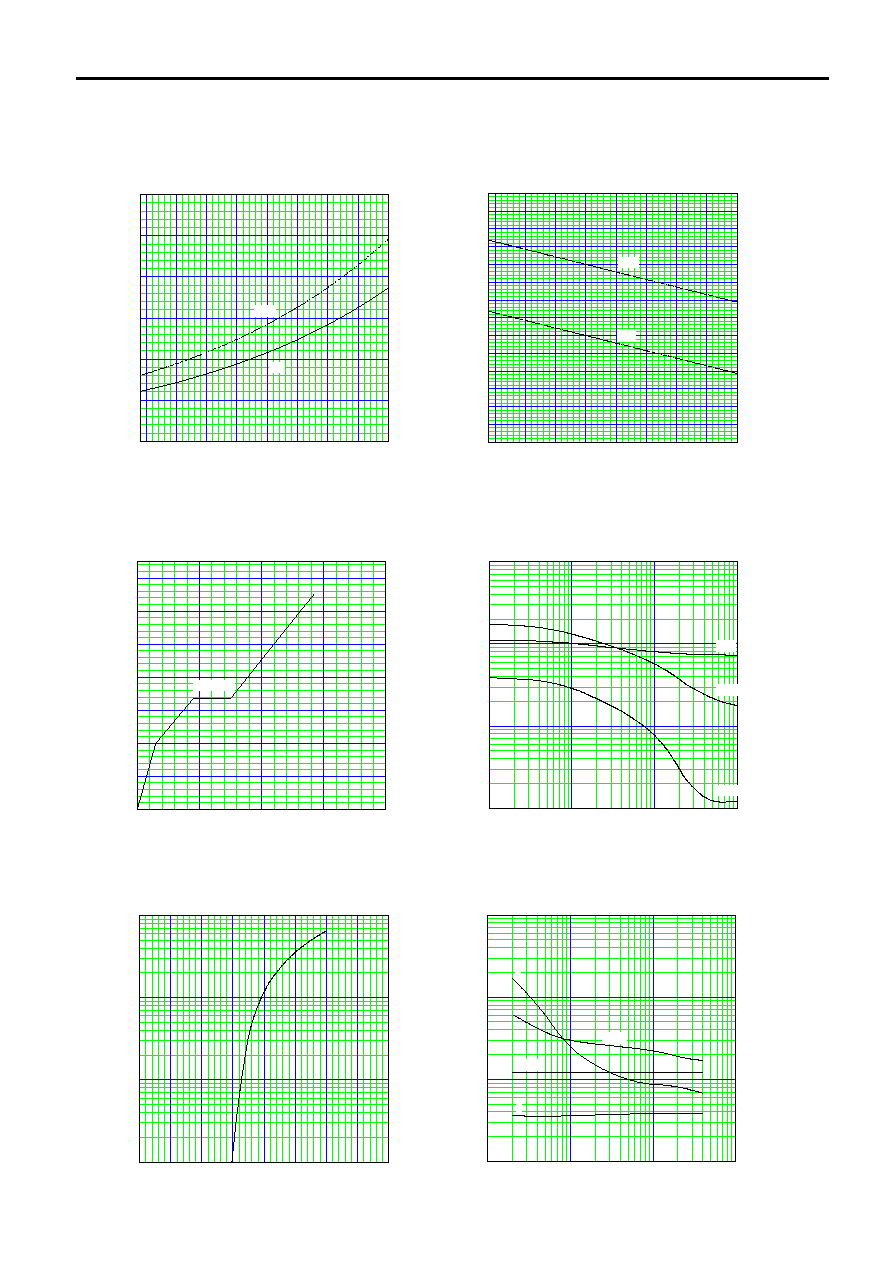
Characteristics
2SK3599-01MR
FUJI POWER MOSFET
ID=f(VGS):80µs Pulse test, VDS=25V,Tch=25∞C
ID=f(VDS):80µs Pulse test,Tch=25∞C
gfs=f(ID):80µs Pulse test, VDS=25V,Tch=25∞C
RDS(on)=f(ID):80µs Pulse test, Tch=25∞C
0
2
4
6
8
10
12
0
20
40
60
80
20V
7.0V
10V
8V
6.5V
7.5V
6.0V
ID [A]
VDS [V]
Typical Output Characteristics
VGS=5.5V
0
1
2
3
4
5
6
7
8
9
10
0.1
1
10
100
ID[A]
VGS[V]
Typical Transfer Characteristic
0.1
1
10
100
0.1
1
10
100
gfs [S]
ID [A]
Typical Transconductance
0
10
20
30
40
50
60
0.00
0.03
0.06
0.09
0.12
0.15
0.18
7.0V
6.5V
RDS(on) [
]
ID [A]
Typical Drain-Source on-state Resistance
10V
20V
8V
7.5V
6.0V
VGS=
5.5V
0
25
50
75
100
125
150
0
5
10
15
20
25
30
35
40
45
50
Allowable Power Dissipation
PD=f(Tc)
PD
[W
]
Tc [
∞
C]
0
25
50
75
100
125
150
0
50
100
150
200
250
300
350
400
I
AS
=12A
I
AS
=17A
I
AS
=29A
EAS
[m
J]
starting Tch [
∞
C]
Maximum Avalanche Energy vs. starting Tch
E(AS)=f(starting Tch):Vcc=48V
3
2SK3599-01MR
FUJI POWER MOSFET
VGS=f(Qg):ID=20A, Tch=25∞C
IF=f(VSD):80µs Pulse test,Tch=25∞C
t=f(ID):Vcc=48V, VGS=10V, RG=10
-50
-25
0
25
50
75
100
125
150
0
25
50
75
100
125
150
RDS(on) [ m
]
Tch [
∞
C]
typ.
max.
Drain-Source On-state Resistance
RDS(on)=f(Tch):ID=10A,VGS=10V
-50
-25
0
25
50
75
100
125
150
0.0
0.5
1.0
1.5
2.0
2.5
3.0
3.5
4.0
4.5
5.0
5.5
6.0
6.5
7.0
max.
min.
Gate Threshold Voltage vs. Tch
VGS(th)=f(Tch):VDS=VGS,ID=250
µ
A
VGS(th) [V]
Tch [
∞
C]
0
10
20
30
40
0
2
4
6
8
10
12
14
Qg [nC]
Typical Gate Charge Characteristics
VGS [V]
Vcc= 50V
10
-1
10
0
10
1
10
2
10
-2
10
-1
10
0
10
1
C [nF]
VDS [V]
Typical Capacitance
C=f(VDS):VGS=0V,f=1MHz
Crss
Coss
Ciss
0.00
0.25
0.50
0.75
1.00
1.25
1.50
1.75
2.00
0.1
1
10
100
IF [A]
VSD [V]
Typical Forward Characteristics of Reverse Diode
10
-1
10
0
10
1
10
2
10
0
10
1
10
2
10
3
Typical Switching Characteristics vs. ID
td(on)
tr
tf
td(off)
t [ns]
ID [A]
4
2SK3599-01MR
FUJI POWER MOSFET
http://www.fujielectric.co.jp/denshi/scd/
10
-8
10
-7
10
-6
10
-5
10
-4
10
-3
10
-2
10
-2
10
-1
10
0
10
1
10
2
Single Pulse
Maximum Avalanche Current Pulsewidth
I
AV
=f(t
AV
):starting Tch=25
∞
C,Vcc=48V
A
v
alan
c
h
e C
u
rr
ent I
AV
[A
]
t
AV
[sec]
10
-6
10
-5
10
-4
10
-3
10
-2
10
-1
10
0
10
-3
10
-2
10
-1
10
0
10
1
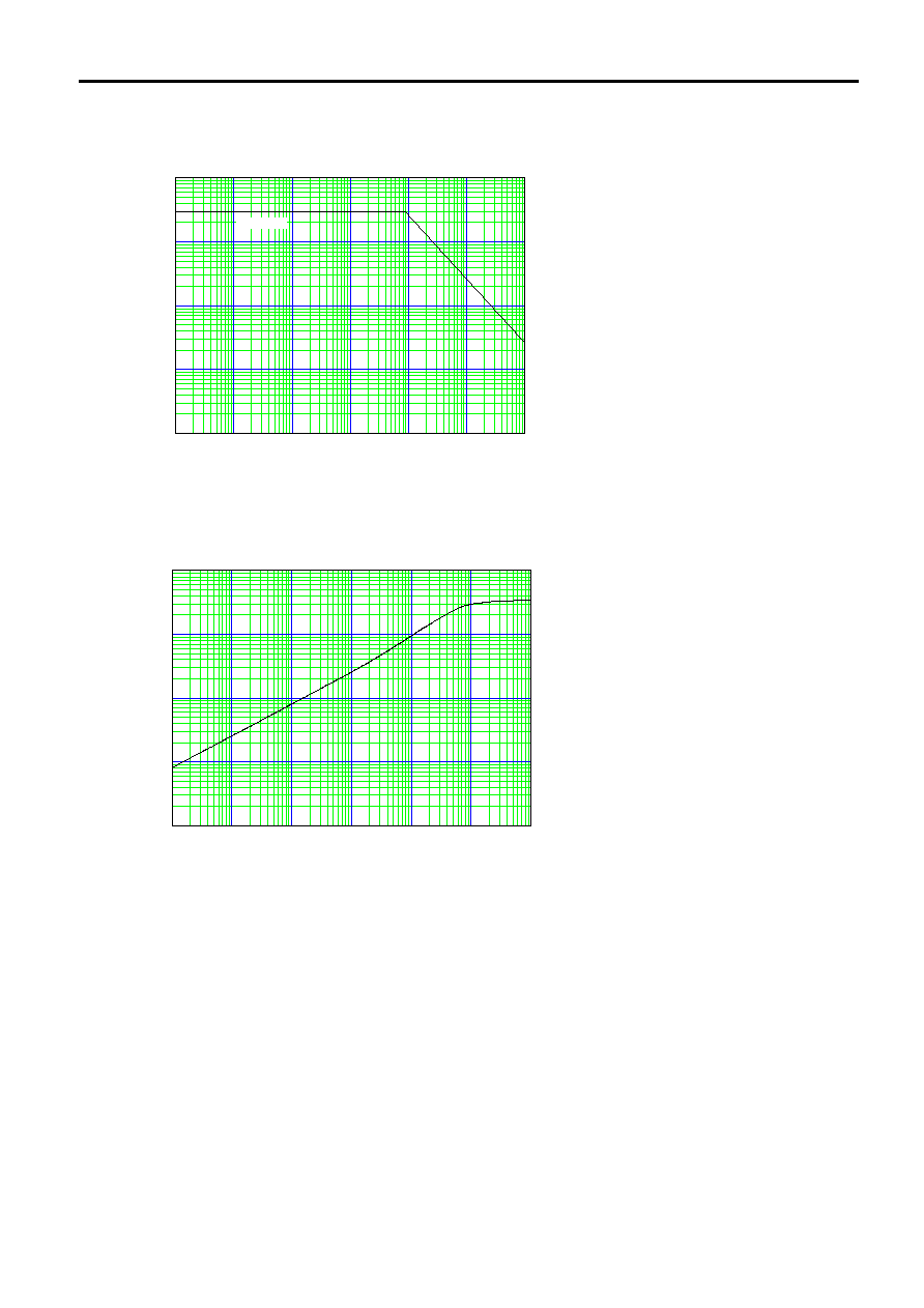
Maximum Transient Thermal Impedance
Zth(ch-c)=f(t):D=0
Zt
h(c
h
-c
) [
∞
C/
W
]
t [sec]