1
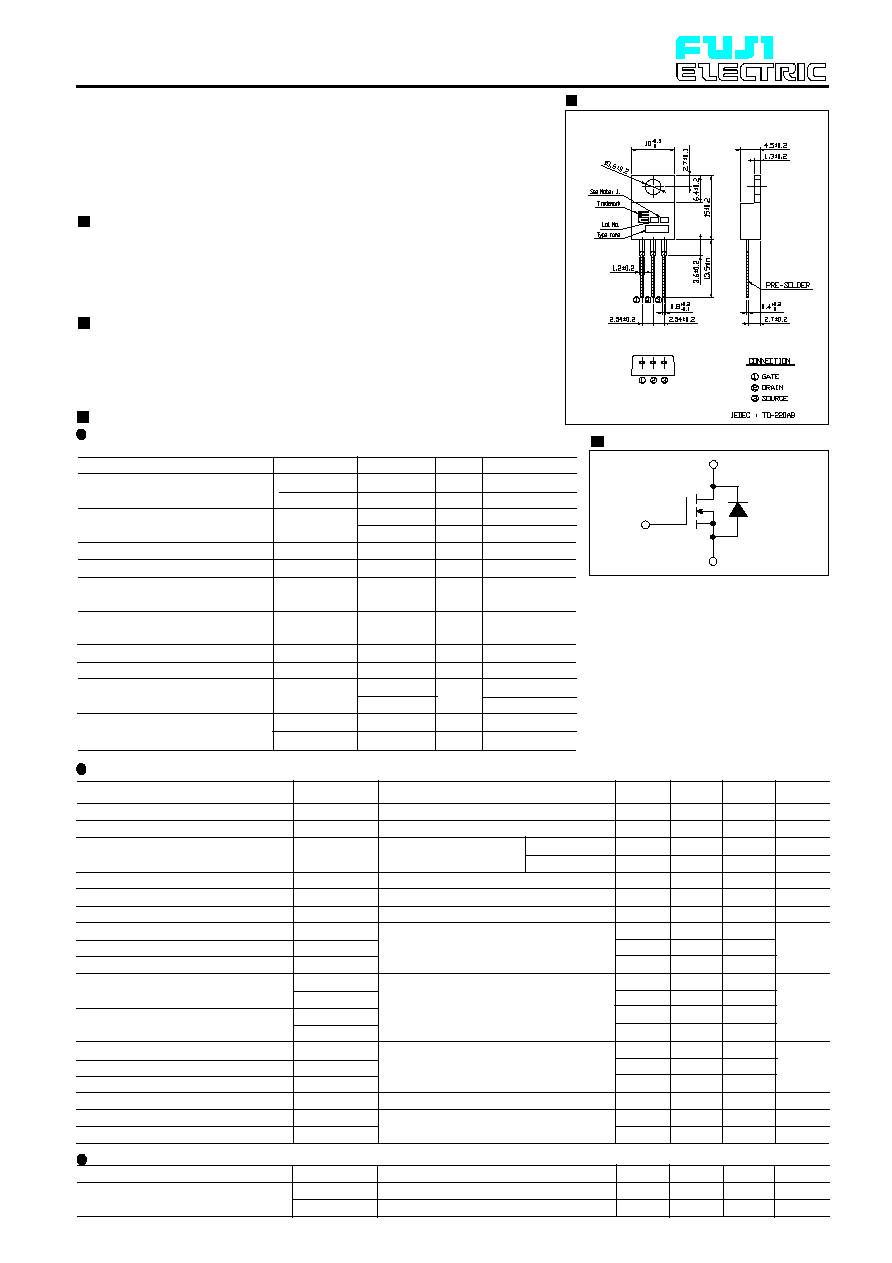
TO-220AB
Item
Symbol
Ratings
Unit Remarks
Drain-source voltage
V
DS
500
V
DSX
500
Continuous Drain Current
I
D
11
Pulsed Drain Current
I
D(puls]
±44
Gate-Source Voltage
V
GS
±30
Maximum Avalanche current
I
AR
11
Non-Repetitive
E
AS
453.9
Maximum Avalanche Energy
Repetitive
E
AR
16.5
Maximum Avalanche Energy
Maximum Drain-Source dV/dt
dV
DS
/dt
20
Peak Diode Recovery dV/dt
dV/dt
5
Max. Power Dissipation
P
D
165
2.02
Operating and Storage
T
ch
+150
Temperature range
T
stg
Electrical characteristics (T
c
=25∞C unless otherwise specified)
Thermalcharacteristics
2SK3931-01
FUJI POWER MOSFET
Maximum ratings and characteristic
Absolute maximum ratings
(Tc=25∞C unless otherwise specified)
Item
Symbol Test Conditions
Zero Gate Voltage Drain Current I
DSS
V
DS
=500V V
GS
=0V
V
DS
=400V V
GS
=0V
V
GS
=±30V
I
D
=5.5A V
GS
=10V
I
D
=5.5A V
DS
=25V
V
CC
=300V I
D
=5.5A
V
GS
=10V
R
GS
=10
Min. Typ. Max. Units
V
V
µA
µA
nA
S
pF
nC
V
ns
µC
ns
Min. Typ. Max. Units
Thermal resistance
R
th(ch-c)
channel to case
R
th(ch-a)
channel to ambient
0.758
62
∞C/W
∞C/W
Symbol
BV
DSS
V
GS(th)
I
GSS
R
DS(on)
g
fs
C
iss
C
oss
C
rss
td
(on)
t
r
td
(off)
t
f
Q
G
Q
GS
Q
GD
V
SD
t
rr
Q
rr
Item
Drain-Source Breakdown Voltaget
Gate Threshold Voltage
Gate-Source Leakage Current
Drain-Source On-State Resistance
Forward Transcondutance
Input Capacitance
Output Capacitance
Reverse Transfer Capacitance
Turn-On Time t
on
Turn-Off Time t
off
Total Gate Charge
Gate-Source Charge
Gate-Drain Charge
Diode forward on-voltage
Reverse recovery time
Reverse recovery charge
Test Conditions
I
D
= 250µA V
GS
=0V
I
D
= 250µA V
DS
=V
GS
T
ch
=25∞C
T
ch
=125∞C
V
DS
=0V
V
DS
=25V
V
GS
=0V
f=1MH
V
CC
=250V
I
D
=11A
V
GS
=10V
I
F
=11A V
GS
=0V T
ch
=25∞C
I
F
=11A V
GS
=0V
-di/dt=100A/µs T
ch
=25∞C
V
V
A
A
V
A
mJ
mJ
kV/µs
kV/µs
W
∞C
∞C
500
3.0
5.0
25
250
10
100
0.57
0.70
4.5
9.0
950
1425
130
195
6.0
9.0
16
24
6.0
9.0
33
50
5.5
8.3
25
38
10
15
8.0
12
1.10
1.50
650
5.5
-55 to +150
Outline Drawings
(mm)
www.fujielectric.co.jp/fdt/scd
Super FAP-G Series
N-CHANNEL SILICON POWER MOSFET
Equivalent circuit schematic
200406
V
GS
=-30V
Note *1
Note *2
Note *3
V
DS
500V
Note *4
Tc=25∞C
Ta=25∞C
=
<
Features
High speed switching Low on-resistance
No secondary breadown Low driving power
Avalanche-proof
Applications
Switching regulators DC-DC converters
UPS (Uninterruptible Power Supply)
Gate(G)
Source(S)
Drain(D)
Note *1:Tch 150∞C,Repetitive and Non-repetitive
Note *2:StartingTch=25∞C,I
AS
=4.4A,L=43mH,
V
CC
=50V,R
G
=50
EAS limited by maximum channel temperature
and avalanch current.
See to the `Avalanche Energy' graph
Note *3:Repetitive rating:Pulse width limited by
maximum channel temperature.
See to the `Transient Theemal impedance'
graph
Note *4:I
F
-I
D
, -di/dt=50A/
µ
s,V
CC
BV
DSS
,Tch 150∞C
=
<
=
<
=
<
=
<

2
Characteristics
2SK3931-01
FUJI POWER MOSFET
0
25
50
75
100
125
150
0
20
40
60
80
100
120
140
160
180
200
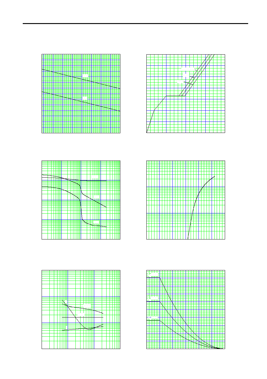
Allowable Power Dissipation
PD=f(Tc)
PD
[W
]
Tc [
∞
C]
0
5
10
15
20
25
30
35
40
0
5
10
15
20
25
30
7.0V
20V
10V
8.0V
6.5V
VGS=6.0V
ID
[
A
]
VDS [V]
Typical Output Characteristics
ID=f(VDS):80
µ
s pulse test,Tch=25
∞
C
0
1
2
3
4
5
6
7
8
9
10
0.1
1
10
100
ID
[
A
]
VGS[V]
Typical Transfer Characteristic
ID=f(VGS):80
µ
s pulse test,VDS=25V,Tch=25
∞
C
0.1
1
10
100
0.1
1
10
100
g
f
s [
S
]
ID [A]
Typical Transconductance
gfs=f(ID):80
µ
s pulse test,VDS=25V,Tch=25
∞
C
0
5
10
15
20
25
30
0.0
0.2
0.4
0.6
0.8
1.0
1.2
1.4
1.6
1.8
2.0
RDS
(
o
n
)
[
]
ID [A]
Typical Drain-Source on-state Resistance
RDS(on)=f(ID):80
µ
s pulse test,Tch=25
∞
C
10V
20V
8.0V
7.0V
6.5V
VGS=6.0V
-50
-25
0
25
50
75
100
125
150
0.0
0.2
0.4
0.6
0.8
1.0
1.2
1.4
1.6
1.8
2.0
RD
S
(
o
n
)
[
]
Tch [
∞
C]
typ.
max.
Drain-Source On-state Resistance
RDS(on)=f(Tch):ID=5.5A,VGS=10V
3
2SK3931-01
FUJI POWER MOSFET
-50
-25
0
25
50
75
100
125
150
0.0
0.5
1.0
1.5
2.0
2.5
3.0
3.5
4.0
4.5
5.0
5.5
6.0
6.5
7.0
max.
min.
Gate Threshold Voltage vs. Tch
VGS(th)=f(Tch):VDS=VGS,ID=250
µ
A
VGS
(
th)
[V]
Tch [
∞
C]
0
10
20
30
40
0
2
4
6
8
10
12
14
Qg [nC]
Typical Gate Charge Characteristics
VGS=f(Qg):ID=11A,Tch=25
∞
C
VGS
[V]
400V
250V
Vcc= 100V
10
-1
10
0
10
1
10
2
10
3
10
0
10
1
10
2
10
3
10
4
C [
p
F]
VDS [V]
Typical Capacitance
C=f(VDS):VGS=0V,f=1MHz
Crss
Coss
Ciss
0.00
0.25
0.50
0.75
1.00
1.25
1.50
0.1
1
10
100
IF
[A]
VSD [V]
Typical Forward Characteristics of Reverse Diode
IF=f(VSD):80
µ
s pulse test,Tch=25
∞
C
10
-1
10
0
10
1
10
2
10
0
10
1
10
2
10
3
Typical Switching Characteristics vs. ID
t=f(ID):Vcc=300V,VGS=10V,RG=10
td(on)
tr
tf
td(off)
t [n
s]
ID [A]
0
25
50
75
100
125
150
0
50
100
150
200
250
300
350
400
450
500
I
AS
=4.4A
I
AS
=6.6A
I
AS
=11A
EAV
[m
J]
starting Tch [
∞
C]
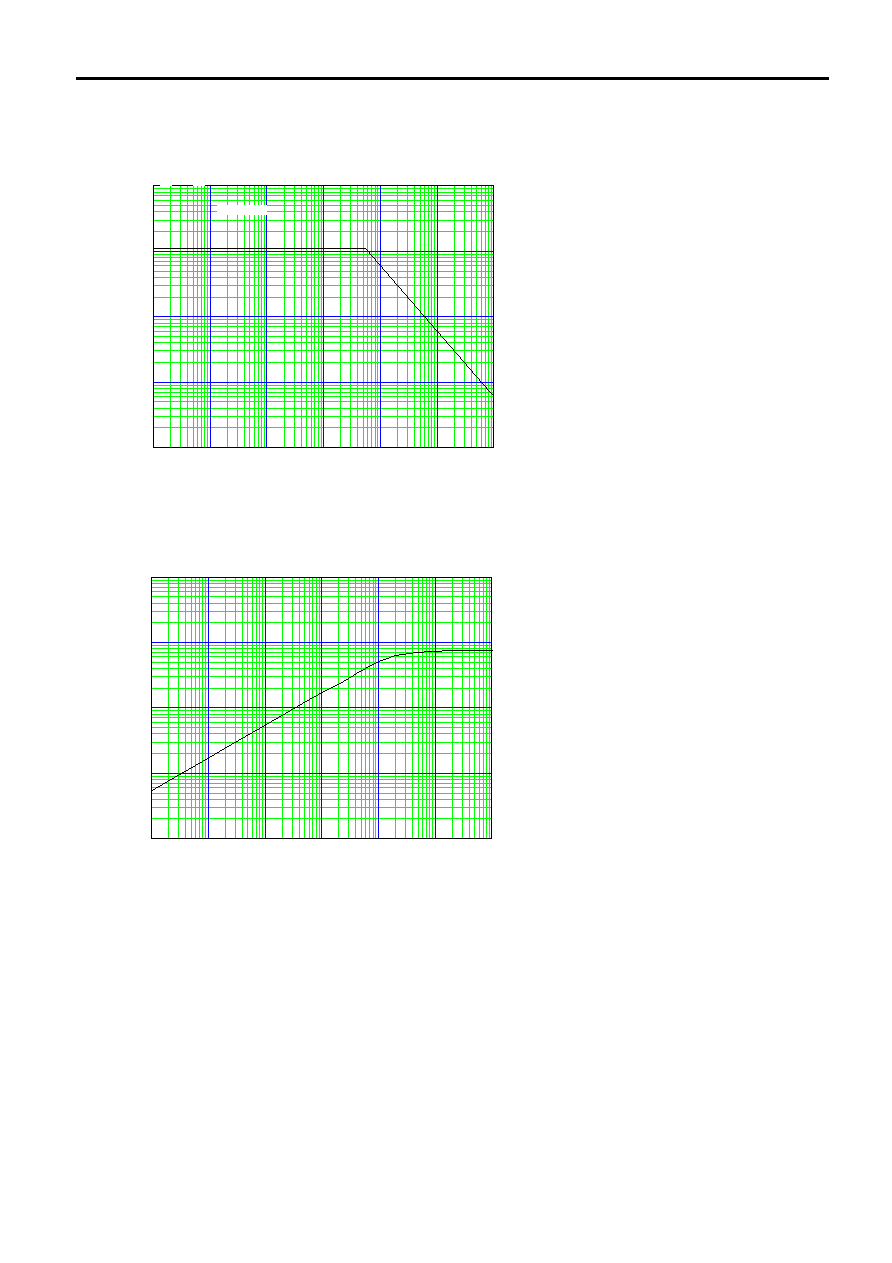
Maximum Avalanche Energy vs. starting Tch
E(AV)=f(starting Tch):Vcc=50V
4
2SK3931-01
FUJI POWER MOSFET
http://www.fujielectric.co.jp/fdt/scd/
10
-8
10
-7
10
-6
10
-5
10
-4
10
-3
10
-2
10
-2
10
-1
10
0
10
1
10
2
Single Pulse
Maximum Avalanche Current Pulsewidth
I
AV
=f(t
AV
):starting Tch=25
∞
C,Vcc=50V
A
v
al
an
c
h
e
Cu
rre
nt
I
AV
[A
]
t
AV
[sec]
10
-6
10
-5
10
-4
10
-3
10
-2
10
-1
10
0
10
-3
10
-2
10
-1
10
0
10
1
Maximum Transient Thermal Impedance
Zth(ch-c)=f(t):D=0
Z
t
h(
c
h
-c
) [
∞
C/
W
]
t [sec]