IGBT MODULE ( N series )
n
n
Features
∑
∑
Including Brake Chopper
∑
Square RBSOA
∑
Low Saturation Voltage
∑
∑
Overcurrent Limiting Function
( ~ 3 Times Rated Current )
n
n
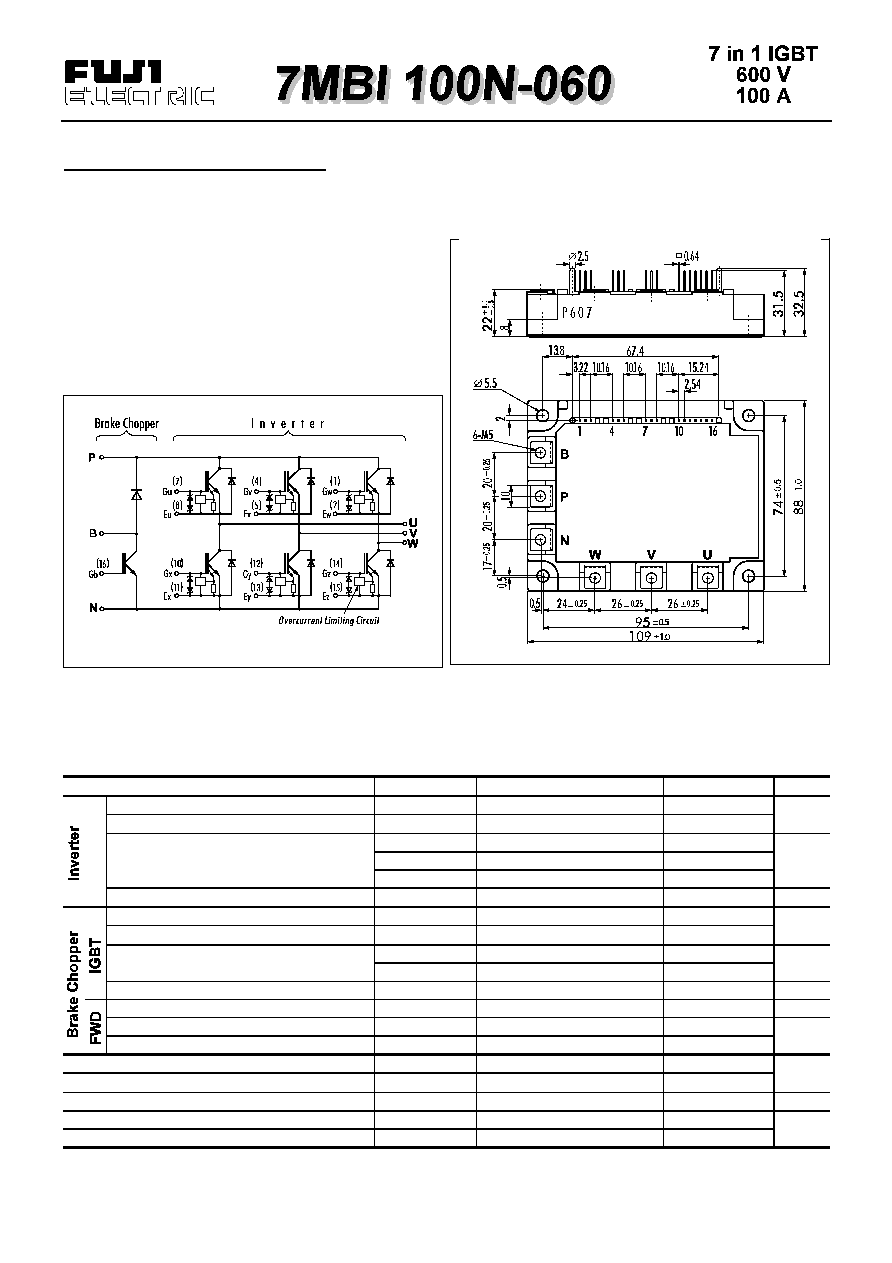
Equivalent Circuit
n
n
Outline Drawing
n
n
Absolute Maximum Ratings
( T
c
=25∞C)
Items
Symbols
Test Conditions
Ratings
Units
Collector-Emitter Voltage
V
CES
600
Gate -Emitter Voltage
V
GES
±
20
I
C
Continuous
100
Collector Current
I
C PULSE
1ms
200
A
-I
C PULSE
Continuous
150
Collector Power Dissipation
P
C
1 device
400
W
Collector-Emitter Voltage
V
CES
600
Gate -Emitter Voltage
V
CES
±
20
I
C
Continuous
50
I
C PULSE
1ms
100
Collector Power Dissipation
P
C
1 device
200
W
Repetitive Peak Reverse Voltage
V
RRM
600
V
Average Forward Current
I
F(AV)
1
Surge Current
I
FSM
10ms
50
Operating Junction Temperature
T
j
+150
Storage Temperature
T
Stg
-40
+125
Isolation Voltage
V
ISO
A.C. 1min.
2500
V
Mounting Screw Torque *
1
3.5
Terminal Screw Torque *
1
3.5
Note: *1:Recommendable Value; 2.5
3.5 Nm (M5)
Collector Current
V
V
A
A
∞C
Nm

n
n
Electrical Characteristics
( T
j
=25∞C )
Items
Symbols
Test Conditions
Min.
Max.
Units
Zero Gate Voltage Collector Current
I
CES
V
GE
=0V V
CE
=600V
3.0
mA
Gate-Emitter Leackage Current
I
GES
V
CE
=0V V
GE
=
±
20V
15
µ
A
Gate-Emitter Threshold Voltage
V
GE(th)
V
GE
=20V I
C
=100mA
4.5
7.5
Collector-Emitter Saturation Voltage
V
CE(sat)
V
GE
=15V I
C
=100A
2.8
Input capacitance
C
ies
f=1MHz, V
GE
=0V, V
CE
=10V
6600 (typ.)
pF
t
on
V
CC
=300V
1.2
I
C
=100A
t
off
V
GE
=
±
15V
1.5
t
f
R
G
= 24
0.35
Diode Forward On-Voltage
V
F
I
F
=100A V
GE
=0V
3.3
V
Reverse Recovery Time
t
rr
I
F
=100A; V
GE
=-10V;
-di
/
dt
=300
A
/
µs
300
ns
Zero Gate Voltage Collector Current
I
CES
V
GE
=0V V
CE
=600V
1.0
mA
Gate-Emitter Leackage Current
I
GES
V
CE
=0V V
GE
=
±
20V
100
nA
Collector-Emitter Saturation Voltage
V
CE(sat)
V
GE
=15V I
C
=50A
2.8
V
t
on
V
CC
=300V
1.2
I
C
= 50A
t
off
V
GE
=
±
15V
1.5
t
f
R
G
= 51
0.35
Reverse Current
I
RRM
V
R
=600V
1.0
mA
Reverse Recovery Time
t
rr
600
ns
n
n
Thermal Characteristics
Items
Symbols
Test Conditions
Min.
Max.
Units
Inverter IGBT
0.31
Thermal Resistance (1 device)
R
th(j-c)
Inverter FRD
0.90
Brake IGBT
0.63
Contact Thermal Resistance
R
th(c-f)
With Thermal Compound
0.05 (typ.)
Turn-on Time
Turn-on Time
Turn-off Time
Turn-off Time
V
µ
s
µ
s
∞C/W
0
50
100
150
10
100
1000
t
f
t
r
t
off
t
on
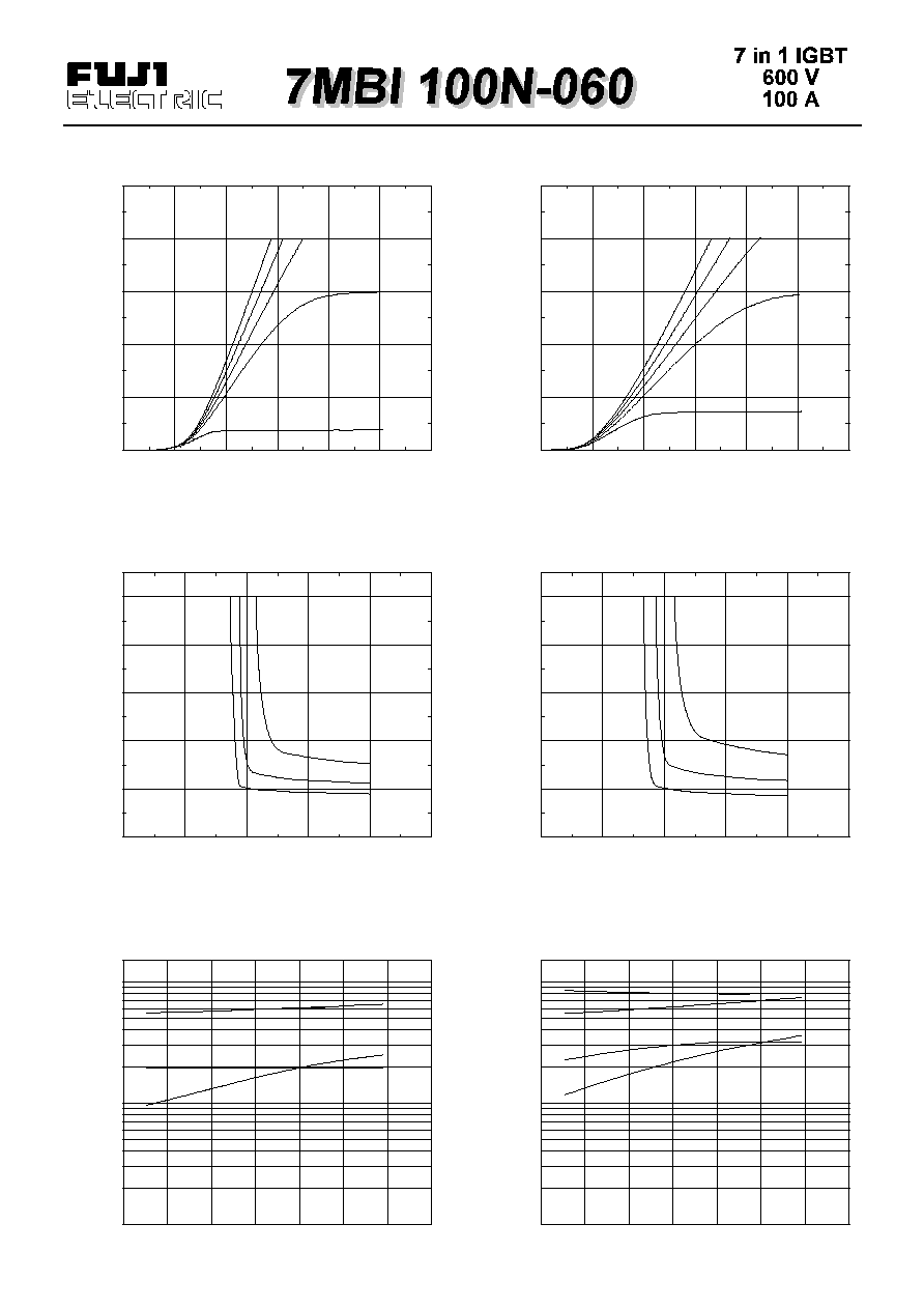
Switching time vs. Collector current
V
CC
=300V, R
G
=24
, V
GE
=±15V, T
j
=25∞C
Switching time : t
on
, t
r
, t
off
, t
f
[nsec]
Collector current : I
C
[A]
0
1
2
3
4
5
6
0
50
100
150
200
250
10V
V
GE
=20V,15V, 12V
Collector-Emitter voltage : V
CE
[V]
Collector current : I
C
[A]
8V
Collector current vs. Collector-Emitter voltage
T
j
=125∞C
0
1
2
3
4
5
6
0
50
100
150
200
250
Collector current vs. Collector-Emitter voltage
T
j
=25∞C
Collector current : I
C
[A]
Collector-Emitter voltage : V
CE
[V]
8V
10V
V
GE
=20V,15V,12V
0
5
10
15
20
25
0
2
4
6
8
10
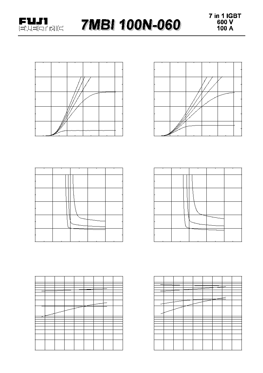
Collector-Emitter vs. Gate-Emitter voltage
T
j
=25∞C
50A
100A
200A
I
C
=
Collector-Emitter voltage : V
CE
[V]
Gate-Emitter voltage : V
GE
[V]
0
5
10
15
20
25
0
2
4
6
8
10
Collector-Emitter vs. Gate-Emitter voltage
T
j
=125∞C
50A
100A
200A
I
C
=
Collector-Emitter voltage : V
CE
[V]
Gate-Emitter voltage : V
GE
[V]
0
50
100
150
10
100
1000
Switching time vs. Collector current
V
CC
=300V, R
G
=24
, V
GE
=±15V, T
j
=125∞C
t
f
t
r
t
on
t
off
Switching time : t
on
, t
r
, t
off
, t
f
[nsec]
Collector current : I
C
[A]

0,001
0,01
0,1
1
0,01
0,1
1
Brake IGBT
IGBT
Diode
Transient thermal resistance
Thermal resistance : R
th(j-c)
[∞C/W]
Pulse width : PW [sec]
0
100
200
300
400
500
600
0
100
200
300
400
500
400V
300V
V
CC
=200V
0
5
10
15
20
25
Dynamic input characteristics
T
j
=25∞C
Collector-Emitter voltage : V
CE
[V]
Gate charge : Q
G
[nC]
10
100
10
100
1000
t
f
t
r
t
off
t
on
Switching time vs. R
G
V
CC
=300V, I
C
=100A, V
GE
=±15V, T
j
=25∞C
Switching time : t
on
, t
r
, t
off
, t
f
[nsec]
Gate resistance : R
G
[
]
0
1
2
3
4
0
50
100
150
200
250
T
j
=125∞C 25∞C
Forward current vs. Forward voltage
V
GE
=OV
Forward current : I
F
[A]
Forward voltage : V
F
[V]
0
50
100
150
10
100
I
rr
25∞C
t
rr
25∞C
t
rr
125∞C
I
rr
125∞C
Reverse recovery characteristics
t
rr
, I
rr
vs. I
F
Reverse recovery current : I
rr
[A]
Reverse recovery time : t
rr
[nsec]
Forward current : I
F
[A]
0
100
200
300
400
500
600
0
200
400
600
800
1000
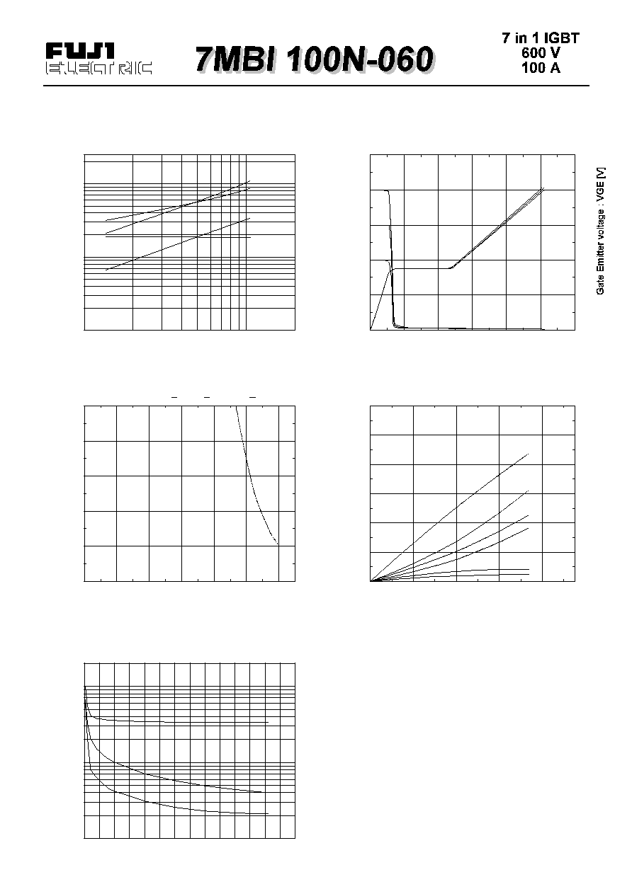
RBSOA (Repetitive pulse)
SCSOA
(non-repetitive pulse)
Reversed biased safe operating area
+V
GE
=15V, -V
GE<
15V, T
j
<125∞C, R
G
>24
Collector current : I
C
[A]
Collector-Emitter voltage : V
CE
[V]

0
5
10
15
20
25
30
35
0,1
1
10
C
res
C
oes
C
ies
Capacitance vs. Collector-Emitter voltage
T
j
=25∞C
Capacitance : C
ies
, C
oes
, C
res
[nF]
Collector-Emitter Voltage : V
CE
[V]
0
50
100
150
200
0
2
4
6
8
10
E
rr
25∞C
E
rr
125∞C
Switching loss vs. Collector current
V
CC
=300V, R
G
=24
, V
GE
=±15V
Switching loss : E
on
, E
off
, E
rr
[mJ/cycle]
Collector Current : I
C
[A]
E
on
25∞C
E
on
125∞C
E
off
25∞C
E
off
125∞C
0
20
40
60
80
10
100
1000
t
f
t
r
t
off
t
on
Switching time vs. Collector current
V
CC
=300V, R
G
=51
, V
GE
±15V, T
j
=25∞C
Switching time : t
on
, t
r
, t
off
, t
f
[nsec]
Collector current : I
C
[A]
0
1
2
3
4
5
0
25
50
75
100
125
10V
V
GE
=20V,15V, 12V
Collector-Emitter voltage : V
CE
[V]
Collector current : I
C
[A]
8V
Collector current vs. Collector-Emitter voltage
T
j
=125∞C
0
1
2
3
4
5
0
25
50
75
100
125
Collector current vs. Collector-Emitter voltage
T
j
=25∞C
Collector current : I
C
[A]
Collector-Emitter voltage : V
CE
[V]
8V
10V
V
GE
=20V,15V,12V
0
5
10
15
20
25
0
2
4
6
8
10
Collector-Emitter vs. Gate-Emitter voltage
T
j
=25∞C
25A
50A
100A
I
C
=
Collector-Emitter voltage : V
CE
[V]
Gate-Emitter voltage : V
G E
[V]
0
5
10
15
20
25
0
2
4
6
8
10
Collector-Emitter vs. Gate-Emitter voltage
T
j
=125∞C
25A
50A
100A
I
C
=
Collector-Emitter voltage : V
CE
[V]
Gate-Emitter voltage : V
G E
[V]
0
20
40
60
80
10
100
1000
Switching time vs. Collector current
V
CC
=300V, R
G
=51
, V
GE
=±15V, T
j
=125∞C
t
f
t
r
t
on
t
off
Switching time : t
on
, t
r
, t
off
, t
f
[nsec]
Collector current : I
C
[A]
Brake Chopper IGBT
0
50
100
150
200
250
300
0
100
200
300
400
500
400V
300V
V
C C
=200V
0
5
10
15
20
25
Dynamic input characteristics
T
j
=25∞C
Collector-Emitter voltage : V
CE
[V]
Gate charge : Q
G
[nC]
10
100
10
100
1000
t
f
t
r
t
off
t
on
Switching time vs. R
G
V
C C
=300V, I
C
=50A, V
G E
=±15V, T
j
=25∞C
Switching time : t
on
, t
r
, t
off
, t
f
[nsec]
Gate resistance : R
G
[
]
0
100
200
300
400
500
600
0
100
200
300
400
500
RBSOA (Repetitive pulse)
S C S O A
(non-repetitive pulse)
Reversed biased safe operating area
+V
G E
=15V, -V
G E
<15V, T
j
<125∞C, R
G
>51
Collector current : I
C
[A]
Collector-Emitter voltage : V
C E
[V]
0
20
40
60
80
0
1
2
3
4
5
6
E
rr
25∞C
E
rr
125∞C
E
on
25∞C
E
on
125∞C
E
off
25∞C
E
off
125∞C
Collector Current : I
C
[A]
Switching loss vs. Collector current
V
C C
=300V, R
G
=51
, V
G E
=±15V
Switching loss : E
on
, E
off
, E
rr
[mJ/cycle]
0
5
10
15
20
25
30
35
0,1
1
10
Capacitance vs. Collector-Emitter voltage
T
j
=25∞C
C
res
C
oes
C
ies
Capacitance : C
ies
, C
oes
, C
res
[nF]
Collector-Emitter Voltage : V
C E
[V]
Brake Chopper IGBT

Fuji Electric GmbH Fuji Electric (UK) Ltd.
Lyoner Straþe 26 Commonwealth House
2 Chalkhill Road Hammersmith
D-60528 Frankfurt/M London W6 8DW, UK
Tel.: 069 - 66 90 29 - 0 Tel.: 0181 - 233 11 30
Fax.: 069 - 66 90 29 - 56 Fax.: 0181 - 233 11 60
P.O. Box 702708 - Dallas, TX 75370 Phone (972) 233-1589 Fax (972) 233-0481 - www.collmer.com
P.O. Box 702708 - Dallas, TX - (972) 733-1700 - (972) 381-9991 (fax)