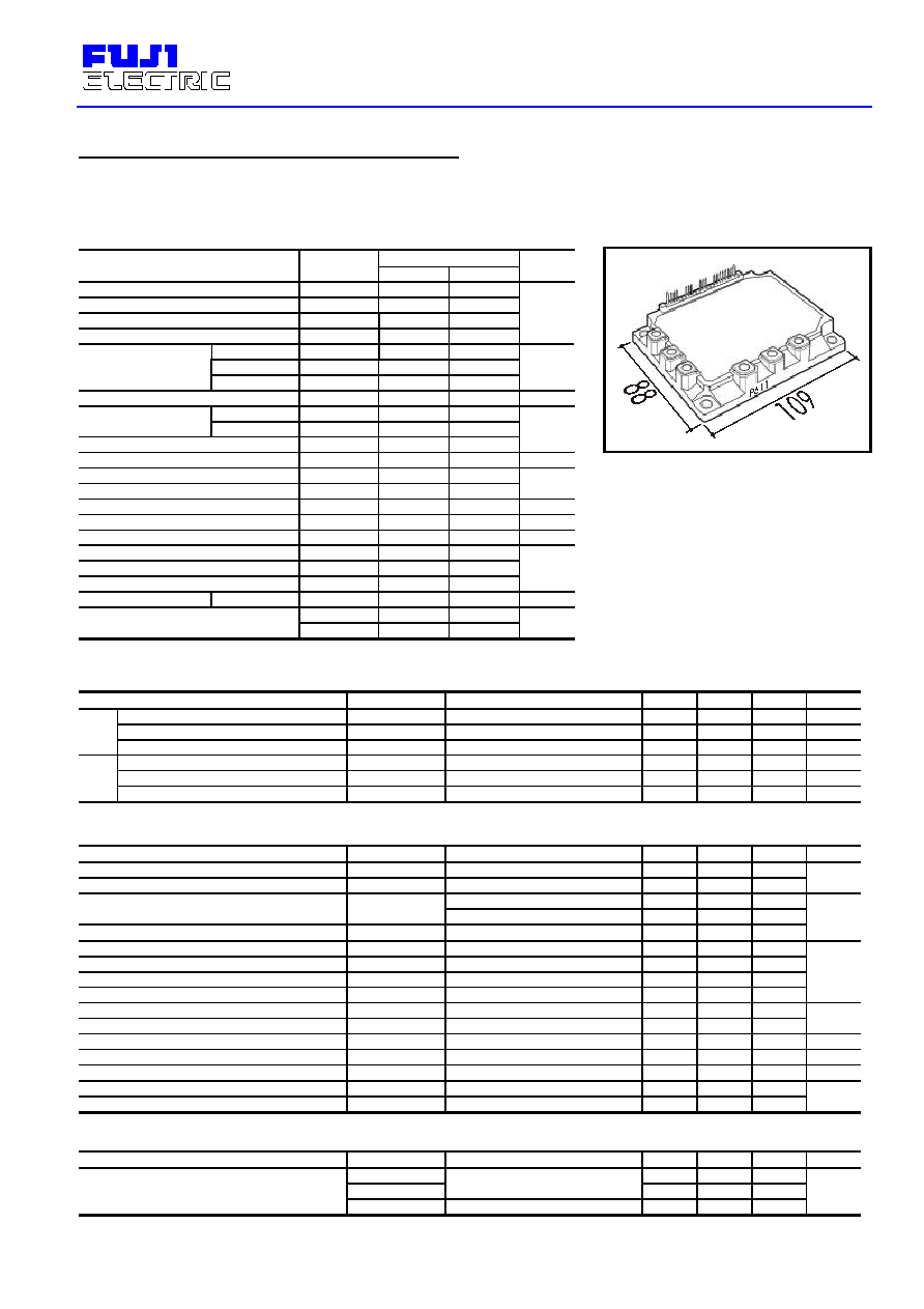
7MBP 50RA-120
IGBT IPM
1200V
6x50A+Chopper
Intelligent Power Module ( R-Series )
n
n
Maximum Ratings and Characteristics
∑
Absolute Maximum Ratings
( T
c
=25∞C
)
Items
Symbols
Ratings
Units
Min.
Max.
DC Bus Voltage
V
DC
0
900
DC Bus Voltage (surge)
V
DC(Surge)
0
1000
DC Bus Voltage (short operating)
V
SC
200
800
Collector-Emitter Voltage
V
CES
0
1200
Inverter
Continuous
I
C
50
Collector
1ms
I
CP
100
A
Current
Duty=62.6%
-I
C
50
Collector Power Dissipation
One Transistor
P
C
400
W
Dynamic Brake
Continuous
I
C
25
Collector Current
1ms
I
CP
50
A
Forward Current of Diode
I
F
25
Collector Power Dissi. DB
One Transistor
P
C
198
W
Voltage of Power Supply for Driver
V
CC
0
20
Input Signal Voltage
V
IN
0
V
Z
Input Signal Current
I
IN
1
mA
Alarm Signal Voltage
V
ALM
0
V
CC
V
Alarm Signal Current
I
ALM
15
mA
Junction Temperature
T
j
150
Operating Temperature
T
OP
-20
100
∞C
Storage Temperature
T
stg
-40
125
Isolation Voltage
A.C. 1min.
V
iso
2500
V
Mounting *1
3.5
Terminals *1
3.5
Note: *1: Recommendable Value; 2.5
3.0 Nm (M5)
∑
Electrical Characteristics of Power Circuit
( at T
j
=25∞C, V
CC
=15V )
Items
Symbols
Conditions
Min.
Typ.
Max.
Units
Collector Current At Off Signal Input
I
CES
V
CE
=1200V,
Input Terminal Open
1.0
mA
INV
Collector-Emitter Saturation Voltage
V
CE(Sat)
I
C
=50A
2.6
V
Forward Voltage of FWD
V
F
-I
C
=50A
3.0
V
Collector Current At Off Signal Input
I
CES
V
CE
=1200V,
Input Terminal Open
1.0
mA
DB
Collector-Emitter Saturation Voltage
V
CE(Sat)
I
C
=25A
2.6
V
Forward Voltage of FWD
V
F
-I
C
=25A
3.3
V
∑
Electrical Characteristics of Control Circuit
( at T
j
=25∞C, V
CC
=15V )
Items
Symbols
Conditions
Min.
Typ.
Max.
Units
Current of P-Line Side Driver
(One Unit)
I
CCP
f
SW
=0~15kHz, T
C
=-20~100∞C
3
18
Current of N-Line Side Driver
(Three Units)
I
CCN
f
SW
=0~15kHz, T
C
=-20~100∞C
10
65
On
1.00
1.35
1.70
Off
1.25
1.60
1.95
V
Input Zener Voltage
V
Z
R
IN
=20k
8.0
Over Heating Protection Temperature Level
T
COH
V
DC
=0V, I
C
=0A, Case Temp.
110
125
Hysteresis
T
CH
20
IGBT Chips Over Heating Protec. Temp. Level
T
jOH
Surface Of IGBT Chip
150
Hysteresis
T
jH
20
Inverter Collector Current Protection Level
I
OC
T
j
=125∞C
75
DB Collector Current Protection Level
I
OC
T
j
=125∞C
38
Over Current Detecting Time
t
DOC
T
j
=25∞C
10
µs
Alarm Signal Hold Time
t
ALM
1.5
2
ms
Limiting Resistor for Alarm
R
ALM
1425
1500
1575
Under Voltage Protection Level
V
UV
11.0
12.5
Hysteresis
V
H
0.2
∑
Dynamic Characteristics
( at T
C
=T
j
=125∞C, V
CC
=15V )
Items
Symbols
Conditions
Min.
Typ.
Max.
Units
t
ON
I
C
=50A, V
DC
=600V
0.3
Switching Time
t
OFF
3.6
µs
t
RR
I
F
=50A, V
DC
=600V
0.4
n
n
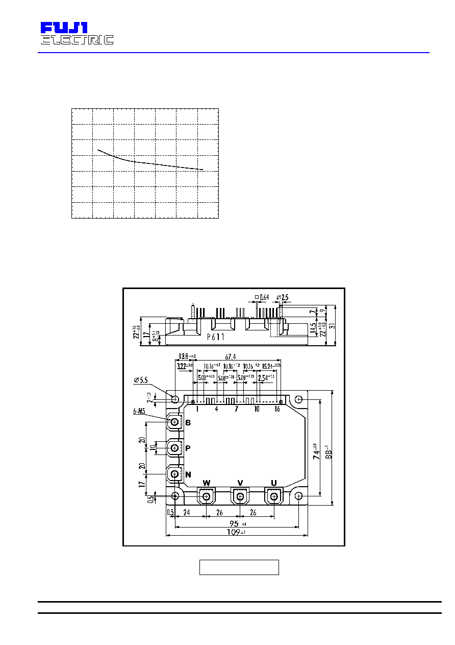
Outline Drawing
Screw Torque
V
IN(th)
Input Signal Threshold Voltage
V
V
Nm
mA
∞C
A
V

7MBP 50RA-120
IGBT IPM
1200V
6x50A+Chopper
∑
Thermal Characteristics
Items
Symbols
Conditions
Min.
Typ.
Max.
Units
R
th(j-c)
Inverter IGBT
0.31
R
th(j-c)
Diode
0.70
R
th(j-c)
DB IGBT
0.63
R
th(c-f)
With Thermal Compound
0.05
n
n
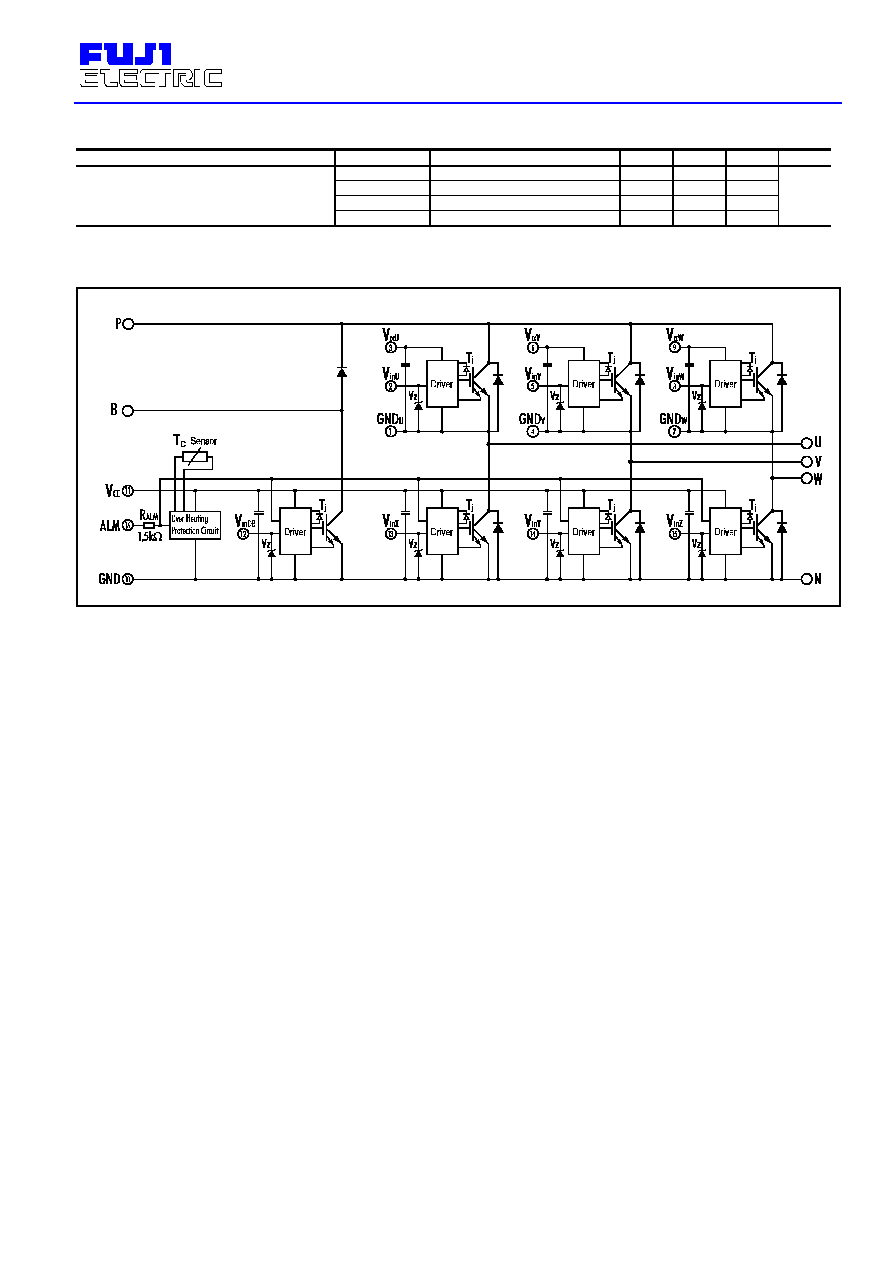
Equivalent Circuit
Drivers include following functions
¿
Short circuit protection circuit
¡
Amplifier for driver
¬
Undervoltage protection circuit
√
Overcurrent protection circuit
ƒ
IGBT Chip overheating protection
Thermal Resistance
∞C/W

7MBP 50RA-120
IGBT IPM
1200V
6x50A+Chopper
n
n
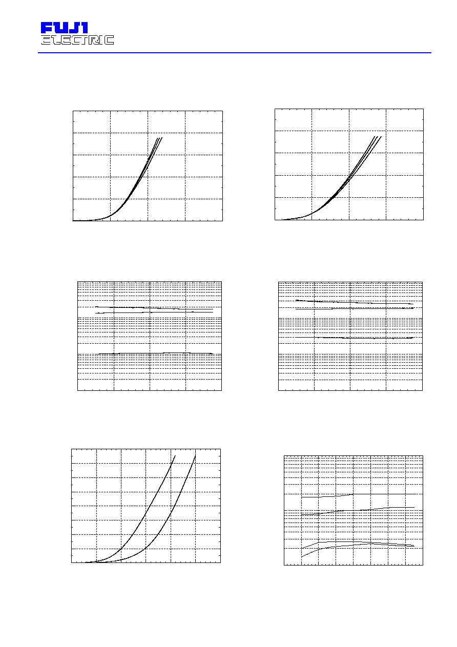
Dynamic Brake
0,0
0,5
1,0
1,5
2,0
2,5
3,0
0
10
20
30
40
50
V
C C
=17V,15V, 13V
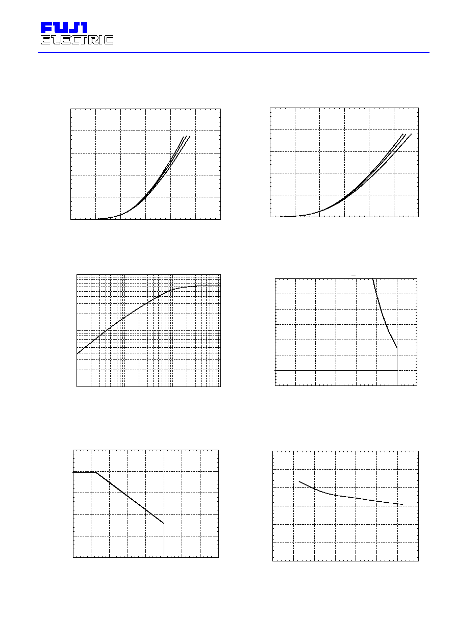
Collector Current vs. Collector-Emitter Voltage
T
j
=25∞C
Collector Current : I
C
[A]
Collector-Emitter Voltage : V
C E
[V]
0,0
0,5
1,0
1,5
2,0
2,5
3,0
0
1 0
2 0
3 0
4 0
5 0
V
C C
= 1 7 V , 1 5 V , 1 3 V
C o llector Current vs. Collector-Emitter Voltage
T
j
= 1 2 5 ∞ C
Collector Current : I
C
[A]
C o llector-Em itter Voltage : V
C E
[V]
10
-3
10
-2
10
-1
10
0
10
-2
10
-1
10
0
IGBT
Transient Thermal Resistance
Thermal Resistance : R
th(j-c)
[∞C/W]
Pulse Width : P
W
[sec]
0
200
400
600
800
1000
1200
1400
0
50
100
150
200
250
300
350
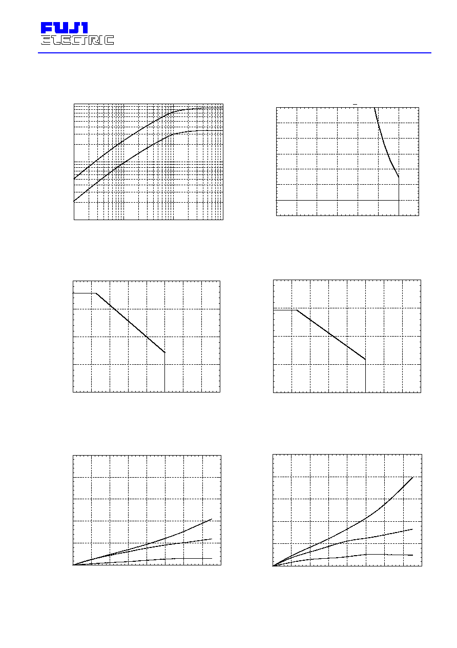
R B S O A
(repetitive pulse)
S C S O A
(non-repetitive pulse)
Reverse Biased Safe Operating Area
V
C C
=15V, T
j
<125∞C
Collector Current : I
C
[A]
Collector-Emitter Voltage : V
C E
[V]
0
2 0
4 0
6 0
8 0
1 0 0
1 2 0
1 4 0
1 6 0
0
5 0
1 0 0
1 5 0
2 0 0
2 5 0
P o w e r D e r a t i n g F o r I G B T
(per device)
Co
llector Power Dissipation : P
C
[W]
C a s e T e m p e r a t u r e : T
C
[∞C]
0
20
40
60
80
1 0 0
1 2 0
1 4 0
0
20
40
60
80
1 0 0
1 2 0
Over Current Protection vs. Junction Temperature
V
cc
=15 V
Over Current Protection Level : I
oc
[A]
Junction Temperature: T
j
[∞C]

7MBP 50RA-120
IGBT IPM
1200V
6x50A+Chopper
n
n
Control Circuit
0
5
1 0
1 5
2 0
2 5
0
5
1 0
1 5
2 0
2 5
3 0
3 5
4 0
V
C C
= 1 7 V
V
C C
= 1 5 V
V
C C
= 1 3 V
V
C C
= 1 7 V
V
C C
= 1 5 V
V
C C
= 1 3 V
P-Side
N-Side
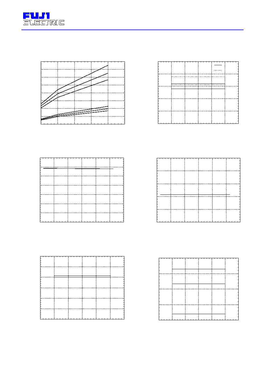
Power Supply Current vs. Switching Frequency
T
j
= 1 0 0 ∞ C
Power Supply Current : I
CC
[mA]
S w itching Frequency : fsw [kHz]
12
13
14
15
16
17
18
0,0
0,5
1,0
1,5
2,0
2,5
T
j
=25∞C
T
j
=125∞C
V
in(on)
V
in(off)
Input Signal Threshold Voltage
vs. Power Supply Voltage
Input Signal Threshold Voltage
: V
in(on)
, V
in(off)
[V]
Power Supply Voltage : V
cc
[V]
20
40
60
80
100
120
140
0
2
4
6
8
10
12
14
Under Voltage vs. Junction Temperature
Under Voltage : V
UV
[V]
Junction Temperature : T
j
[∞C]
20
40
60
80
100
120
140
0,0
0,2
0,4
0,6
0,8
1,0
Under Voltage Hysterisis vs. Junction Temperature
Under Voltage Hysterisis : V
H
[V]
Junction Temperature: T
j
[∞C]
12
13
14
15
16
17
18
0,0
0,5
1,0
1,5
2,0
2,5
3,0
T
j
=25∞C
T
j
=125∞C
Alarm Hold Time vs. Power Supply Voltage
Alarm Hold Timen : t
ALM
[ms]
Power Supply Voltage : V
cc
[V]
12
13
14
15
16
17
18
0
50
100
150
200
T
cH
,T
jH
T
cOH
T
jOH
Over Heating Characteristics
T
cOH
, T
jOH
, T
cH
, T
jH
vs. V
cc
Over Heating Protection : T
cOH
, T
jOH
[∞C]
Over Heating Hysterisis : T
cH
, T
jH
[∞C]
Power Supply Voltage : V
cc
[V]

7MBP 50RA-120
IGBT IPM
1200V
6x50A+Chopper
n
n
Inverter
0
1
2
3
4
0
2 0
4 0
6 0
8 0
1 0 0
V
C C
= 1 7 V , 1 5 V , 1 3 V
C o llector Current vs. Collector-Emitter Voltage
T
j
= 2 5 ∞ C
Collector Current : I
C
[A]
C o llector-Em itter Voltage : V
C E
[V]
0
1
2
3
4
0
20
40
60
80
100
V
C C
=17V,15V, 13V
Collector Current vs. Collector-Emitter Voltage
T
j
=125∞C
Collector Current : I
C
[A]
Collector-Emitter Voltage : V
C E
[V]
0
20
40
60
80
10
100
1000
10000
t
f
t
off
t
on
Switching Time vs. Collector Current
V
D C
=600V, V
C C
=15V, T
j
=25∞C
Switching Time : t
on
, t
r
, t
off
, t
f
[ns]
C o llector Current : I
C
[A]
0
20
40
60
80
10
100
1000
10000
t
f
t
off
t
on
Switching Time vs. Collector Current
V
D C
=300V, V
C C
=15V, T
j
=125∞C
Switching Time : t
on
, t
r
, t
off
, t
f
[ns]
C o llector Current : I
C
[A]
0,0
0,5
1,0
1,5
2,0
2,5
3,0
0
10
20
30
40
50
60
70
80
25∞C
T
j
=125∞C
Forward Voltage vs. Forward Current
Forward Current : I
F
[A]
Forward Voltage : V
F
[V]
0
10
20
30
40
50
60
70
80
10
100
1000
I
rr
=25∞C
t
rr
=25∞C
I
rr
=125∞C
t
rr
=125∞C
Reverse Recovery Characteristics
t
rr
, I
rr
vs. I
F
Reverse Recovery Current : I
rr
[A]
Reverse Recovery Time : t
rr
[ns]
Forward Current : I
F
[A]

7MBP 50RA-120
IGBT IPM
1200V
6x50A+Chopper
n
n
Inverter
10
-3
10
-2
10
-1
10
0
10
-2
10
-1
10
0
IGBT
FWD
Transient Thermal Resistance
Thermal Resistance : R
th(j-c)
[∞C/W]
Pulse Width : P
W
[sec]
0
200
400
600
800
1000
1200
1400
0
100
200
300
400
500
600
700
R B S O A
(repetitive pulse)
S C S O A
(non-repetitive pulse)
Reverse Biased Safe Operating Area
V
C C
=15V, T
j
<125∞C
Collector Current : I
C
[A]
Collector-Emitter Voltage : V
C E
[V]
0
20
40
60
80
100
120
140
160
0
100
200
300
400
Power Derating For IGBT
(per device)
Collector Power Dissipation : P
C
[W]
Case Temperature : T
C
(∞C)
0
20
40
60
80
100
120
140
160
0
50
100
150
200
Power Derating For FWD
(per device)
Collector Power Dissipation : P
C
[W]
Case Temperature : T
C
(∞C)
0
1 0
2 0
3 0
4 0
5 0
6 0
7 0
8 0
0
5
1 0
1 5
2 0
2 5
E
rr
E
off
E
on
S w itching Loss vs. Collector Current
V
D C
= 6 0 0 V , V
C C
=15V, T
j
= 2 5 ∞ C
Switching Loss : E
on
, E
off
, E
rr
[mJ/cycle]
Collector Current : I
C
[A]
0
10
20
30
40
50
60
70
80
0
5
10
15
20
25
E
rr
E
off
E
on
Switching Loss vs. Collector Current
V
D C
=600V, V
C C
=15V, T
j
=125∞C
Switching Loss : E
on
, E
off
, E
rr
[mJ/cycle]

7MBP 50RA-120
IGBT IPM
1200V
6x50A+Chopper
n
n
Inverter
0
2 0
4 0
6 0
8 0
1 0 0
1 2 0
1 4 0
0
4 0
8 0
1 2 0
1 6 0
2 0 0
2 4 0
2 8 0
Over Current Protection vs. Junction Temperature
V
cc
= 1 5 V
Over Current Protection Level : I
oc
[A]
Junction Temperature: T
j
[∞C]
n
n
Outline Drawing
Weight: 440g
Specification is subject to change without notice
October 98
