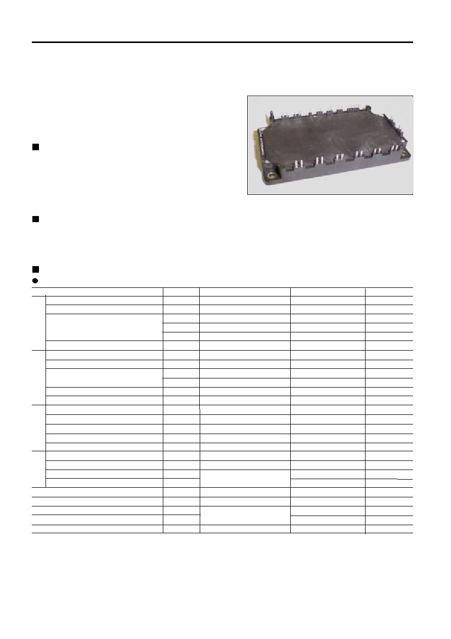
7MBR75SD060
IGBT Modules
PIM/Built-in converter with thyristor
and brake (S series)
600V / 75A / PIM
Features
∑ Low V
CE
(sat)
∑ Compact Package
∑ P.C. Board Mount Module
∑ Converter Diode Bridge Dynamic Brake Circuit
Applications
∑ Inverter for Motor Drive
∑ AC and DC Servo Drive Amplifier
∑ Uninterruptible Power Supply
Maximum ratings and characteristics
Absolute maximum ratings (Tc=25∞C unless without specified)
Item Symbol Condition Rating Unit
Collector-Emitter voltage
Gate-Emitter voltage
Collector current
Collector power disspation
Collector-Emitter voltage
Gate-Emitter voltage
Collector current
Collector power disspation
Repetitive peak reverse voltage(Diode)
Repetitive peak off-state voltage
Repetitive peak reverse voltage
Average on-state current
Surge 0n-state current (Non-Repetitive)
Junction temperature
Repetitive peak reverse voltage
Average output current
Surge current (Non-Repetitive)
I
2
t (Non-Repetitive)
Converter Thyristor Brake Inverter
Junction temperature (except Thyristor)
Storage temperature
Isolation between terminal and copper base *2
voltage between thermistor and others *3
Mounting screw torque
V
CES
V
GES
I
C
I
CP
-I
C
P
C
V
CES
V
GES
I
C
I
CP
P
C
V
RRM
V
DRM
V
RRM
I
T(AV)
I
TSM
T
jw
V
RRM
I
O
I
FSM
I
2
t
T
j
T
stg
V
iso
Continuous
1ms
1 device
Continuous
1ms
1 device
50Hz/60Hz sine wave
Tj=125∞C, 10ms half sine wave
50Hz/60Hz sine wave
Tj=150∞C, 10ms
half sine wave
AC : 1 minute
600
±20
75
150
75
300
600
±20
50
100
200
600
800
800
75
750
125
800
75
525
1378
+150
-40 to +125
AC 2500
AC 2500
1.7 *
1
V
V
A
A
A
W
V
V
A
A
W
V
V
V
A
A
∞C
V
A
A
A
2
s
∞C
∞C
V
V
N∑m
*1
Recommendable value : 1.3 to 1.7 N∑m (M4)
*2 All terminals should be connected together when isolation test will be done.
*3 Terminal 8 and 9 should be connected together. Terminal 1 to 7 and 10 to 26
should be connected together and shorted to copper base.
Electrical characteristics (Tj=25∞C unless otherwise specified)
Item Symbol Condition Characteristics Unit
Min. Typ. Max.
Zero gate voltage collector current
Gate-Emitter leakage current
Gate-Emitter threshold voltage
Collector-Emitter saturation voltage
Input capacitance
Turn-on time
Turn-off
Forward on voltage
Reverse recovery time of FRD
Zero gate voltage collector current
Gate-Emitter leakage current
Collector-Emitter saturation voltage
Turn-on time
Turn-off time
Reverse current
off-state current
Reverse current
Gate trigger current
Gate trigger voltage
On-state voltage
Forward on voltage
Reverse current
Resistance
B value
Thyristor Converter
Thyristor Brake Inverter
I
CES
I
GES
V
GE(th)
V
CE(sat)
C
ies
t
on
t
r
t
off
t
f
V
F
t
rr
I
CES
I
GES
V
CE(sat)
t
on
t
r
t
off
t
f
I
RRM
I
DM
I
RRM
I
GT
V
GT
V
TM
V
FM
I
RRM
R
B
V
CE
=600V, V
GE
=0V
V
CE
=0V, V
GE
=±20V
V
CE
=20V, I
C
=75mA
V
GE
=15V, Ic=75A chip
terminal
V
GE
=0V, V
CE
=10V, f=1MHz
V
CC
=300V
I
C
=75A
V
GE
=±15V
R
G
=33
I
F
=75A chip
terminal
I
F
=75A
V
CES
=600V, V
GE
=0V
V
CE
=0V, V
GE
=±20V
I
C
=50A, V
GE
=15V chip
terminal
V
CC
=300V
I
C
=50A
V
GE
=±15V
R
G
=51
V
R
=600V
V
DM
=800V
V
RM
=800V
V
D
=6V, I
T
=1A
V
D
=6V, I
T
=1A
I
TM
=75A chip
terminal
I
F
=75A chip
terminal
V
R
=800V
T=25∞C
T=100∞C
T=25/50∞C
200
200
8.5
2.55
1.2
0.6
1.0
0.35
2.7
300
200
200
2.55
1.2
0.6
1.0
0.35
200
1.0
1.0
100
2.5
1.18
1.5
200
7500
5.5 7.8
µA
nA
V
V
pF
µs
V
ns
µA
nA
V
µs
µA
mA
mA
mA
V
V
V
µA
K
Item Symbol Condition Characteristics Unit
Min. Typ. Max.
Inverter IGBT
Inverter FWD
Brake IGBT
Thyristor
Converter Diode
With thermal compound
0.42
0.90
0.63
0.56 ∞C/W
0.70
0.05
Thermal resistance ( 1 device ) Rth(j-c)
Contact thermal resistance * Rth(c-f)
Thermal resistance Characteristics
IGBT Module
7MBR75SD060
* This is the value which is defined mounting on the additional cooling fin with thermal compound
1.8
2.1
0.45
0.25
0.40
0.05
1.7
2.0
1.8
2.05
0.45
0.25
0.40
0.05
1.1
1.2
1.1
1.2
5000
465 495 520
3305 3375 3450

IGBT Module
7MBR75SD060
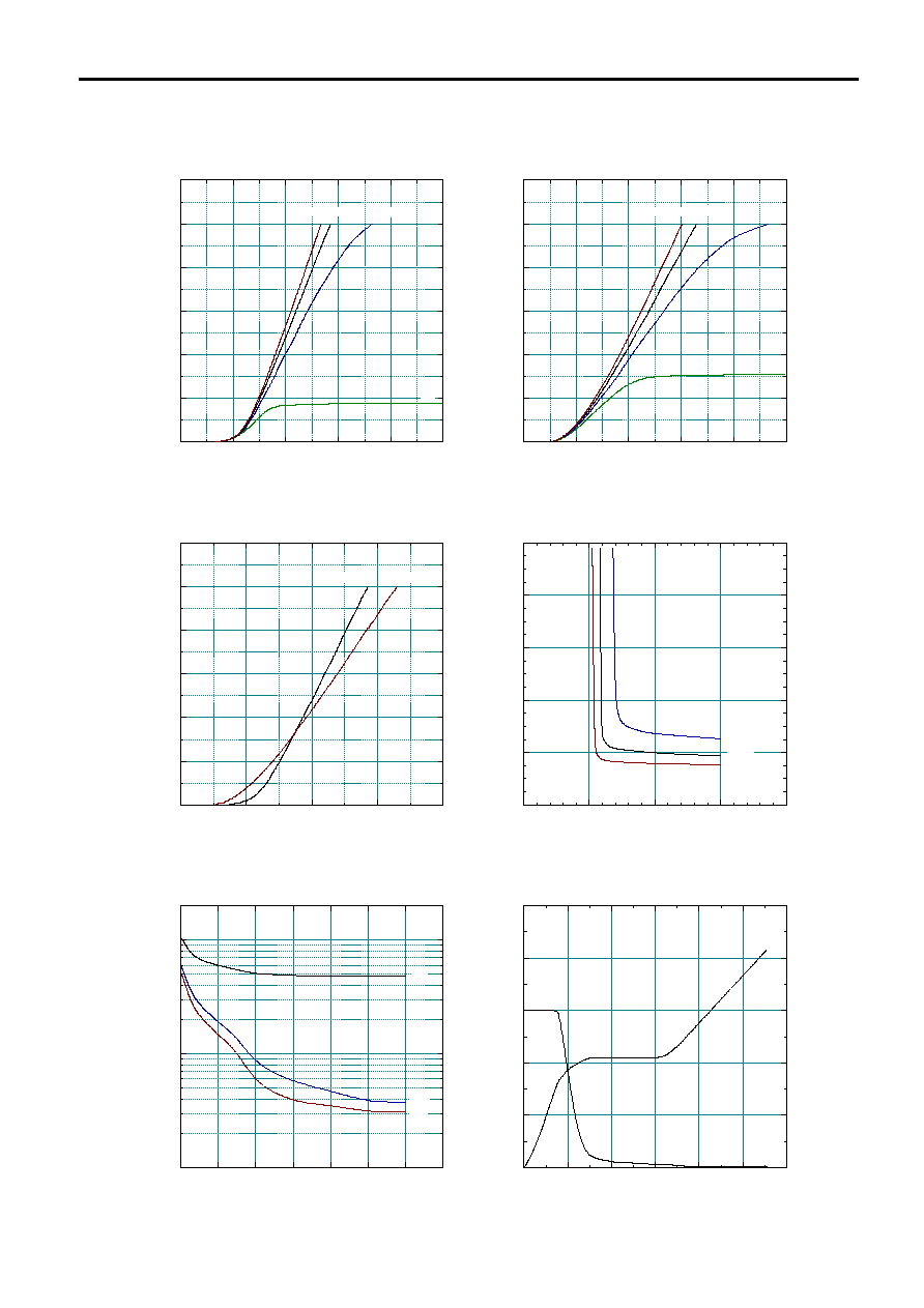
Characteristics (Representative)
0
1
2
3
4
5
0
50
100
150
200
10V
12V
15V
VGE= 20V
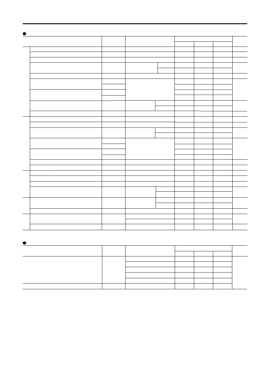
[ Inverter ]
Collector current vs. Collector-Emitter voltage
Tj= 25∞C(typ.)
C
o
lle
c
t
or
c
u
rr
e
n
t
: Ic
[ A ]
Collector - Emitter voltage : VCE [ V ]
0
1
2
3
4
5
0
50
100
150
200
10V
12V
15V
VGE= 20V
[ Inverter ]
Collector current vs. Collector-Emitter voltage
Tj= 125∞C(typ.)
Collector - Emitter voltage : VCE [ V ]
C
o
lle
c
t
or
c
u
rr
e
n
t
: Ic
[ A ]
0
1
2
3
4
0
50
100
150
200
Tj= 25∞C
Tj= 125∞C
[ Inverter ]
Collector current vs. Collector-Emitter voltage
VGE=15V (typ.)
Collector - Emitter voltage : VCE [ V ]
C
o
lle
c
t
or
c
u
rr
e
n
t
: Ic
[ A ]
5
10
15
20
25
0
2
4
6
8
10
Ic= 37.5A
Ic= 75A
Ic=150A
[ Inverter ]
Collector-Emitter voltage vs. Gate-Emitter voltage
Tj= 25∞C(typ.)
C
o
l
l
e
c
t
o
r
-
E
m
i
t
te
r
v
o
l
t
a
g
e
:
V
C
E
[
V
]
Gate - Emitter voltage : VGE [ V ]
0
5
10
15
20
25
30
35
100
1000
10000
30000
[ Inverter ]
Capacitance vs. Collector-Emitter voltage (typ.)
VGE=0V, f= 1MHz, Tj= 25∞C
C
a
p
a
c
i
t
a
n
c
e
:
C
i
e
s
,
C
o
e
s
, C
r
e
s
[ p
F
]
Collector - Emitter voltage : VCE [ V ]
Coes
Cres
Cies
0
100
200
300
400
500
0
100
200
300
400
500
[ Inverter ]
Dynamic Gate charge (typ.)
Vcc=300V, Ic=75A, Tj= 25∞C
Gate charge : Qg [ nC ]
C
o
l
l
e
c
t
o
r
-
E
m
i
t
te
r
v
o
l
t
a
g
e
:
V
C
E
[
V
]
0
5
10
15
20
25
G
a
t
e
-
E
m
it
ter
v
o
l
t
a
g
e
:
V
G
E [ V ]
IGBT Module
7MBR75SD060
0
50
100
150
10
100
1000
ton
tr
toff
tf
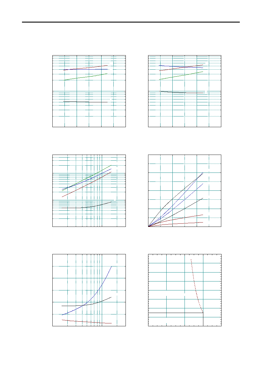
[ Inverter ]
Switching time vs. Collector current (typ.)
Vcc=300V, VGE=±15V, Rg=33
, Tj= 25∞C
S
w
i
t
chi
n
g
ti
m
e
:
to
n,
tr
, t
o
f
f
, t
f
[ ns
e
c
]
Collector current : Ic [ A ]
0
50
100
150
10
100
1000
tf
tr
ton
toff
[ Inverter ]
Switching time vs. Collector current (typ.)
Vcc=300V, VGE=±15V, Rg= 33
, Tj= 125∞C
Collector current : Ic [ A ]
S
w
i
t
chi
n
g
ti
m
e
:
to
n,
tr
, t
o
f
f
, t
f
[ ns
e
c
]
10
100
300
10
100
1000
5000
toff
ton
tr
tf
[ Inverter ]
Switching time vs. Gate resistance (typ.)
Vcc=300V, Ic=75A, VGE=±15V, Tj= 25∞C
Gate resistance : Rg [
]
S
w
i
t
chi
n
g
ti
m
e
:
to
n,
tr
, t
o
f
f
, t
f
[ ns
e
c
]
0
50
100
150
0
2
4
6
8
Err(25∞C)
Eoff(25∞C)
Eon(25∞C)
Err(125∞C)
Eoff(125∞C)
Eon(125∞C)
[ Inverter ]
Switching loss vs. Collector current (typ.)
Vcc=300V, VGE=±15V, Rg=33
S
w
i
t
chi
n
g
l
o
s
s
:
E
o
n
,
E
o
f
f
,
E
r
r
[
m
J
/pul
se
]
Collector current : Ic [ A ]
10
100
300
0
5
10
15
[ Inverter ]
Switching loss vs. Gate resistance (typ.)
Vcc=300V, Ic=75A, VGE=±15V, Tj= 125∞C
S
w
i
t
chi
n
g
l
o
s
s
:
E
o
n
,
E
o
f
f
,
E
r
r
[
m
J
/pul
se
]
Gate resistance : Rg [
]
Eon
Err
Eoff
0
200
400
600
800
0
100
200
300
400
500
600
700
800
SCSOA
(non-repetitive pulse)
RBSOA
(Repetitive pulse)
[ Inverter ]
Reverse bias safe operating area
+VGE=15V, -VGE<=15V, Rg>=33
, Tj<=125∞C
Collector - Emitter voltage : VCE [ V ]
Co
l
l
e
c
t
o
r
cur
r
e
n
t
:
Ic
[
A
]
IGBT Module
7MBR75SD060
0
1
2
3
0
50
100
150
200
0.0
0.4
0.8
1.2
1.6
2.0
2
5
10
100
200
Tj=25∞C
Tj=125∞C
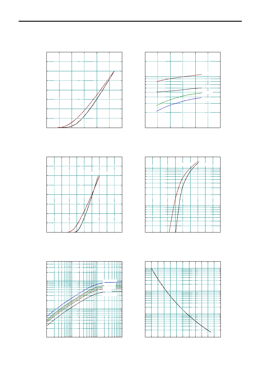
[ Inverter ]
Forward current vs. Forward on voltage (typ.)
F
o
r
w
a
r
d
c
u
r
r
e
n
t
:
IF
[
A ]
Forward on voltage : VF [ V ]
0
50
100
150
10
100
300
Irr(125∞C)
Irr(25∞C)
trr(25∞C)
trr(125∞C)
[ Inverter ]
Reverse recovery characteristics (typ.)
Vcc=300V, VGE=±15V, Rg=33
Forward current : IF [ A ]
R
e
v
e
r
s
e
r
e
c
o
v
e
r
y
c
u
r
r
e
n
t
:
Ir
r
[ A
]
R
e
v
e
r
s
e
r
e
c
o
v
e
r
y
t
i
m
e
: t
r
r
[
n
s
e
c
]
0.0
0.4
0.8
1.2
1.6
2.0
0
50
100
150
200
Tj= 25∞C
Tj= 125∞C
[ Converter ]
Forward current vs. Forward on voltage (typ.)
Forward on voltage : VFM [ V ]
F
o
r
w
a
r
d
c
u
r
r
e
n
t
:
IF
[
A ]
0.001
0.01
0.1
1
0.01
0.1
1
5
IGBT[Inverter]
Conv. Diode
Transient thermal resistance
T
h
e
r
m
a
l
r
e
s
i
st
a
n
se
:
R
t
h
(
j
-
c)
[
∞
C
±
/
W
]
Pulse width : Pw [ sec ]
FWD[Inverter]
Thyristor
IGBT[Brake]
-60
-40
-20
0
20
40
60
80
100 120 140 160 180
0.1
1
10
100
200
[ Thermistor ]
Temperature characteristic (typ.)
Temperature [ ∞C ]
R
e
s
i
s
t
a
n
c
e
: R
[
k
]
[ Thyristor ]
On-state current vs. On-state voltage (typ.)
Tjw= 125∞C
Tjw= 25∞C
Ins
t
a
n
t
a
ne
o
u
s
o
n
-
s
t
a
te
c
u
r
r
e
n
t
[ A
]
Instantaneous on-state voltage [ V ]
IGBT Module
7MBR75SD060
0
1
2
3
4
5
0
20
40
60
80
100
120
10V
12V
15V
VGE= 20V
[ Brake ]
Collector current vs. Collector-Emitter voltage
Tj= 25∞C(typ.)
C
o
lle
c
t
or
c
u
rr
e
n
t : Ic
[
A ]
Collector - Emitter voltage : VCE [ V ]
0
1
2
3
4
5
0
20
40
60
80
100
120
10V
12V
15V
VGE= 20V
[ Brake ]
Collector current vs. Collector-Emitter voltage
Tj= 125∞C(typ.)
Collector - Emitter voltage : VCE [ V ]
C
o
lle
c
t
or
c
u
rr
e
n
t : Ic
[
A ]
0
1
2
3
4
0
20
40
60
80
100
120
Tj= 25∞C
Tj= 125∞C
[ Brake ]
Collector current vs. Collector-Emitter voltage
VGE=15V (typ.)
Collector - Emitter voltage : VCE [ V ]
C
o
lle
c
t
or
c
u
rr
e
n
t : Ic
[
A ]
5
10
15
20
25
0
2
4
6
8
10
Ic= 25A
Ic= 50A
Ic=100A
[ Brake ]
Collector-Emitter voltage vs. Gate-Emitter voltage
Tj= 25∞C(typ.)
C
o
l
l
e
c
t
o
r
-
Em
i
t
t
e
r
v
o
l
t
a
g
e
:
VC
E
[
V ]
Gate - Emitter voltage : VGE [ V ]
0
5
10
15
20
25
30
35
100
1000
10000
20000
[ Brake ]
Capacitance vs. Collector-Emitter voltage (typ.)
VGE=0V, f= 1MHz, Tj= 25∞C
C
a
pa
c
i
ta
n
c
e
:
C
i
e
s
,
C
o
e
s
, C
r
e
s
[ pF
]
Collector - Emitter voltage : VCE [ V ]
Coes
Cres
Cies
0
50
100
150
200
250
300
0
100
200
300
400
500
[ Brake ]
Dynamic Gate charge (typ.)
Vcc=300V, Ic=50A, Tj= 25∞C
Gate charge : Qg [ nC ]
C
o
l
l
e
c
t
o
r
-
Em
i
t
t
e
r
v
o
l
t
a
g
e
:
VC
E
[
V ]
0
5
10
15
20
25
G
a
t
e
-
E
m
it
ter
v
o
lt
a
g
e
:
V
G
E [ V
]
IGBT Module
7MBR75SD060
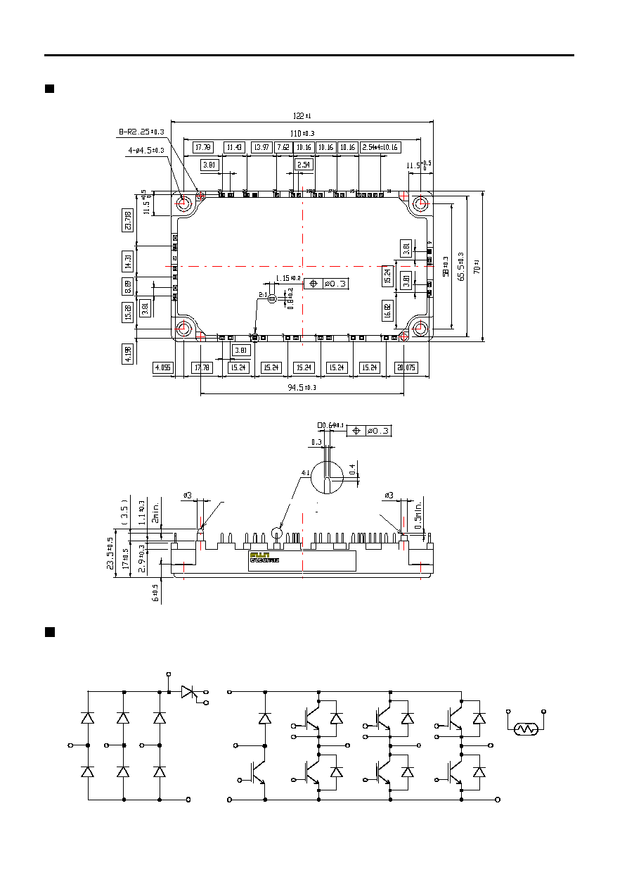
Outline Drawings, mm
Equivalent Circuit Schematic
Marking : White
Marking : White
23(N)
2(S)
3(T)
1(R)
21
(P)
26
25
22(P1)
7(B)
24(N1)
13(Gx)
19(Eu)
20
(Gu)
18
(Gv )
17(Ev )
4(U)
12(Gy )
11(Gz)
5(V)
15(Ew)
16
(Gw)
6(W)
10(En)
9
8
[ Converter ]
[ Thyristor ]
[ Brake ]
[ Inverter ]
[ Thermistor ]
14(Gb)
23(N)
2(S)
3(T)
1(R)
21
(P)
26
25
22(P1)
7(B)
24(N1)
13(Gx)
19(Eu)
20
(Gu)
18
(Gv )
17(Ev )
4(U)
12(Gy )
11(Gz)
5(V)
15(Ew)
16
(Gw)
6(W)
10(En)
9
8
[ Converter ]
[ Thyristor ]
[ Brake ]
[ Inverter ]
[ Thermistor ]
14(Gb)