 | –≠–ª–µ–∫—Ç—Ä–æ–Ω–Ω—ã–π –∫–æ–º–ø–æ–Ω–µ–Ω—Ç: E413511 | –°–∫–∞—á–∞—Ç—å:  PDF PDF  ZIP ZIP |

DS04-13511-2E
FUJITSU SEMICONDUCTOR
DATA SHEET
Linear IC Converter
CMOS
D/A Converter for Digital Tuning
(12-channel, 8-bit, on-chip OP amp, low-voltage)
MB88346L
s
DESCRIPITON
The Fujitsu MB88346L is an 8-bit D/A converter capable of low-voltage operation, and designed with a built-in
amp on each of its 12 analog output lines for large-current drive capability.
The use of serial data input means that only three control lines are required, and enables cascade connection
of multiple MB88346L chips.
The MB88346L is suitable for applications such as electronic volume controls and replacement of semi-fixed
resistors in tuning systems.
In addition, the MB88346L is both function-compatible and pin-compatible with the MB88346B now in use,
allowing easy substitution of the MB88346L for reduced supply voltage.
s
FEATURES
∑ Low voltage operation (V
CC
/V
DD
: 2.7 to 3.6 V)
∑ Ultra-low power consumption (0.5 mW/ch at V
CC
= 3 V)
∑ Ultra-compact space-saving package lineup (SSOP-20)
∑ Contains 12-channel R-2R type 8-bit D/A converter
∑ On-chip analog output amps (sink current max. 1.0 mA, source current max. 1.0 mA)
∑ Analog output range from 0 to V
CC
∑ Two separate power supply/ground lines for MCU interface block/operational amplifier output buffer block and
D/A converter block
∑ Serial data input, maximum operating speed 2.5 MHz
∑ (maximum operating speed in cascade connection is 1.5 MHz)
∑ CMOS process
∑ Package lineup includes DIP 20-pin, SOP 20-pin, SSOP 20-pin.
s
PACKAGES
(DIP-20P-M02)
20-pin plastic SOP
(FPT-20P-M01)
(FPT-20P-M03)
20-pin plastic DIP
20-pin plastic SSOP

2
MB88346L
s
PIN ASSIGNMENT
1
2
3
4
5
6
7
8
9
10
GND
AO
2
AO
1
DI
CLK
LD
DO
AO
12
AO
11
V
CC
20
19
18
17
16
15
14
13
12
11
V
SS
AO
3
AO
4
AO
5
AO
6
AO
7
AO
8
AO
9
AO
10
V
DD
(Top view)
(DIP-20P-M02)
(FPT-20P-M01)
(FPT-20P-M03)

3
MB88346L
s
PIN DESCRIPTION
Pin No.
Symbol
I/O
Function
17
DI
I
Serial address/data input to the internal 12-bit shift register: The
address/data format is that upper 4 bits (D11 to D8) indicate an
address and lower 8 bits (D7 to D0) indicate data. The D11 (MSB) is
the first-in bit and D0 (LSB) is the last-in bit.
14
DO
O
Outputs MSB bit data from 12-bit shift register.
16
CLK
I
Shift clock input to the internal 12-bit shift register: At the rising edge
of CLK data on the DI pin is shifted into the LSB of the shift register
and contents of the shift register are shifted right (to the MSB).
15
LD
I
Load strobe input for a 12-bit address/data: A high level on the LD pin
latches a 4-bit address (upper 4 bits: D11 to D8) of the internal 12-bit
shift register into the internal address decoder, and writes 8-bit data
(lower 8 bits: D7 to D0) of the shift register into an internal data latch
selected by the latched address.
18
19
2
3
4
5
6
7
8
9
12
13
AO
1
AO
2
AO
3
AO
4
AO
5
AO
6
AO
7
AO
8
AO
9
AO
10
AO
11
AO
12
O
8-bit D/A output pins with OP amps.
11
V
CC
--
MCU interface and OP amp power supply pin.
20
GND
--
MCU interface and OP amp ground pin.
10
V
DD
--
D/A converter power supply pin.
1
V
SS
--
D/A converter ground pin.

4
MB88346L
s
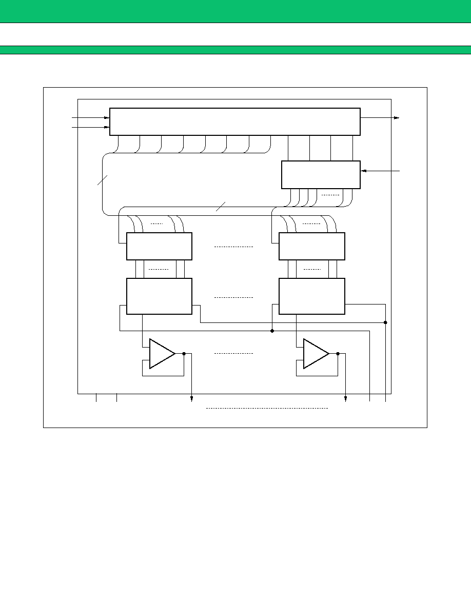
BLOCK DIAGRAM
12-bit shift register
D0
D1
D2
D3
D4
D5
D6
D7
D8
D9
D10
D11
Address decoder
8-bit latch
8-bit
R-2R
D/A converter
8-bit latch
8-bit
R-2R
D/A converter
12
1
D7
D0
D7
D0
12
1
8
+
≠
AO
12
V
DD
V
SS
AO
1
GND
V
CC
LD
DO
DI
CLK
+
≠
12
2 3
4

5
MB88346L
s
DATA CONFIGURATION
The MB88346L has a 12-bit shift register for chip control functions. The 12-bit shift register must be used to set
up data in the configuration shown below.
The data configuration has a total of 12 bits, four for address selection and eight for D/A data output.
1. Shift Register Control Data Configuration
2. D/A Converter Control Signals
V
LB
= (V
DD
≠ V
SS
)/255
D0
D1
D2
D3
D4
D5
D6
D7
D/A data output
0
0
0
0
0
0
0
0
V
SS
1
0
0
0
0
0
0
0
V
LB
+ V
SS
0
1
0
0
0
0
0
0
V
LB
◊
2 + V
SS
∑
∑
∑
∑
∑
∑
∑
∑
∑
∑
∑
∑
∑
∑
∑
∑
∑
∑
∑
∑
∑
∑
∑
∑
∑
∑
∑
0
1
1
1
1
1
1
1
V
LB
◊
254 + V
SS
1
1
1
1
1
1
1
1
V
DD
Last
LSB
D0
D1
D2
D3
D4
D5
D6
D7
D8
D9
D10
D11
First
MSB
Address selection
D/A data output

6
MB88346L
3. Address Selection Signals
D8
D9
D10
D11
Address selection
0
0
0
0
Don't Care
0
0
0
1
AO
1
selection
0
0
1
0
AO
2
selection
0
0
1
1
AO
3
selection
0
1
0
0
AO
4
selection
0
1
0
1
AO
5
selection
0
1
1
0
AO
6
selection
0
1
1
1
AO
7
selection
1
0
0
0
AO
8
selection
1
0
0
1
AO
9
selection
1
0
1
0
AO
10
selection
1
0
1
1
AO
11
selection
1
1
0
0
AO
12
selection
1
1
0
1
Don't Care
1
1
1
0
Don't Care
1
1
1
1
Don't Care

7
MB88346L
s
OPERATING DESCRIPTION
1. Timing Chart for Data Condition Setup
2. Analog Output Voltage Range
DI
CLK
LD
D/A data output
D11
D10
D9
D8
D2
D1
D0
MSB
LSB
R-2R ladder output
OP amp output
V
DD
V
CC
GND
V
SS
V
CC
= V
DD
GND = V
SS
D/A output range (linear range)
V
AOH
(V
CC
)
V
AOL
(GND)

8
MB88346L
s
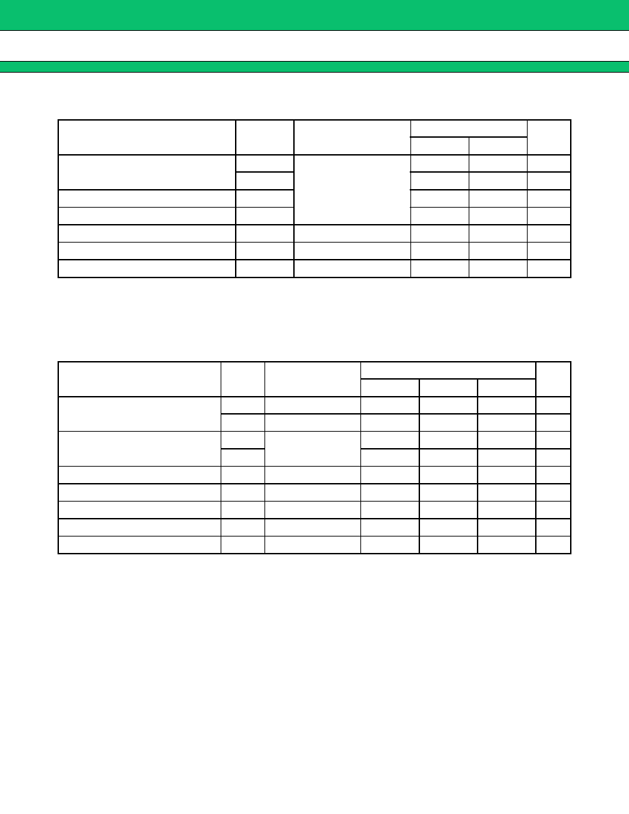
ABSOLUTE MAXIMUM RATINGS
* : V
CC
V
DD
WARNING: Semiconductor devices can be permanently damaged by application of stress (voltage, current,
temperature, etc.) in excess of absolute maximum ratings. Do not exceed these ratings.
s
RECOMMENDED OPERATING CONDITIONS
WARNING: The recommended operating conditions are required in order to ensure the normal operation of the
semiconductor device. All of the device's electrical characteristics are warranted when the device is
operated within these ranges.
Always use semiconductor devices within their recommended operating condition ranges. Operation
outside these ranges may adversely affect reliability and could result in device failure.
No warranty is made with respect to uses, operating conditions, or combinations not represented on
the data sheet. Users considering application outside the listed conditions are advised to contact their
FUJITSU representatives beforehand.
Prameter
Symbol
Condition
Rating
Unit
Min.
Max.
Power supply voltage
V
CC
GND used as reference,
Ta = 25
∞
C
≠0.3
+7.0
V
V
DD
*
≠0.3
+7.0
V
Input voltage
V
IN
≠0.3
V
CC
+ 0.3
V
Output voltage
V
OUT
≠0.3
V
CC
+ 0.3
V
Power consumption
P
D
--
--
250
mW
Operating temperature
Ta
--
≠20
+85
∞
C
Storage temperature
Tstg
--
≠55
+150
∞
C
Prameter
Symbol
Condition
Value
Unit
Min.
Typ.
Max.
Power supply voltage 1
V
CC
--
2.7
--
3.6
V
GND
--
--
0
--
V
Power supply voltage 2
V
DD
V
DD
≠ V
SS
2.0 V
2.0
--
V
CC
V
V
SS
GND
--
V
CC
≠ 2.0
V
Analog output source current
I
AL
V
CC
= 3.0 V
--
--
1.0
mA
Analog output sink current
I
AH
V
CC
= 3.0 V
--
--
1.0
mA
Oscillator limiting output capacity
C
AL
--
--
--
0.1
µ
F
Digital data value range
--
--
#00
--
#FF
--
Operating temperature
Ta
--
≠20
--
+85
∞
C

9
MB88346L
s
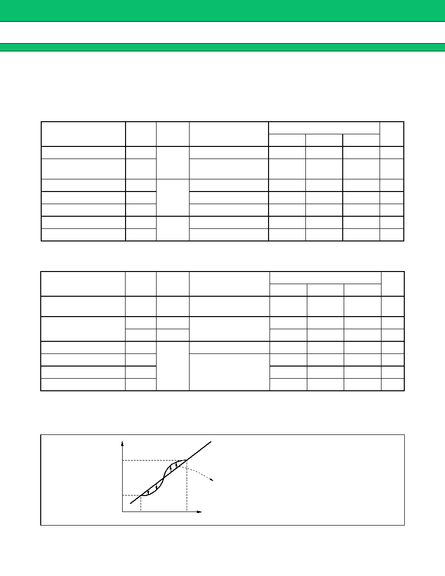
ELECTRICAL CHARACTERISTICS
1. DC Characteristics
(1) Digital Block
(V
DD
, V
CC
= +2.7 V to 3.6 V (V
CC
V
DD
), GND = V
SS
= 0 V, Ta = ≠20
∞
C to +85
∞
C)
(2) Analog Block 1
(V
DD
, V
CC
= +2.7 V to 3.6 V (V
CC
V
DD
), GND = V
SS
= 0 V, Ta = ≠20
∞
C to +85
∞
C)
Nonlinearity error:
Deviation (error) in input/output curves with respect to an ideal straight line connecting
output voltage at "00" and output voltage at "FF."
Differential linearity error: Deviation (error) in amplification with respect to theoretical increase in amplification
per 1-bit increase in digital value.
Prameter
Symbol
Pin
Condition
Value
Unit
Min.
Typ.
Max.
Power supply voltage
V
CC
V
CC
--
2.7
3.0
3.6
V
Power supply current 1
I
CC
Stationary (CLK signal
stopped), no load
--
1.2
3.0
mA
Input leak current
I
ILK
CLK, DI,
LD
V
IN
= 0 to V
CC
≠10
--
10
µ
A
L level input voltage
V
IL
--
--
--
0.2 V
CC
V
H level input voltage
V
IH
--
0.8 V
CC
--
--
V
L level output voltage
V
OL
DO
I
OL
= 2.5 mA
--
--
0.4
V
H level output voltage
V
OH
I
OH
= ≠400
µ
A
V
CC
≠ 0.4
--
--
V
Prameter
Symbol
Pin
Condition
Value
Unit
Min.
Typ.
Max.
Power consumption
I
DD
V
DD
Maximum setting value
from #00 to #FF
--
0.6
1.5
mA
Analog voltage
V
DD
V
DD
V
DD
≠ V
SS
2.0
2.0
--
V
CC
V
V
SS
V
SS
GND
--
V
CC
≠ 2.0
V
Resolution
Res
AO
1
to
AO
12
--
--
8
--
bits
Monotonic increase
Rem
V
DD
V
CC
≠ 0.1 V,
V
SS
0.1 V, no load
--
8
--
bits
Nonlinearity error
LE
≠1.5
--
1.5
LSB
Differential linearity error
D
LE
≠1.0
--
1.0
LSB
V
AOH
V
AOL
#
00
#
FF
Analog output
Ideal straight line
Non linearity error
Digital setting
Note: The value of V
AOH
and V
DD
, and
the value of V
AOL
and V
SS
are not
necessarily equivalent.

10
MB88346L
(3) Analog Block 2
(V
DD
, V
CC
= +2.7 V to 3.6 V (V
CC
V
DD
), GND = V
SS
= 0 V, Ta = ≠20
∞
C to +85
∞
C)
Prameter
Symbol
Pin
Condition
Value
Unit
Min.
Typ.
Max.
Output minimum
voltage 1
V
AOL1
AO
1
to
AO
12
V
DD
= V
CC
= 3.0 V,
V
SS
= GND = 0.0 V,
I
AL
= 0
µ
A
Digital data = #00
V
SS
--
V
SS
+ 0.1
V
Output minimum
voltage 2
V
AOL2
V
DD
= V
CC
= 3.0 V,
V
SS
= GND = 0.0 V,
I
AL
= 500
µ
A
Digital data = #00
V
SS
≠ 0.2
V
SS
V
SS
+ 0.2
V
Output minimum
voltage 3
V
AOL3
V
DD
= V
CC
= 3.0 V,
V
SS
= GND = 0.0 V,
I
AH
= 500
µ
A
Digital data = #00
V
SS
--
V
SS
+ 0.2
V
Output minimum
voltage 4
V
AOL4
V
DD
= V
CC
= 3.0 V,
V
SS
= GND = 0.0 V,
I
AL
= 1.0 mA
Digital data = #00
V
SS
≠ 0.3
V
SS
V
SS
+ 0.3
V
Output minimum
voltage 5
V
AOL5
V
DD
= V
CC
= 3.0 V,
V
SS
= GND = 0.0 V
I
AH
= 1.0 mA
Digital data = #00
V
SS
--
V
SS
+ 0.3
V
Output maximum
voltage 1
V
AOH1
V
DD
= V
CC
= 3.0 V,
V
SS
= GND = 0.0 V,
I
AL
= 0
µ
A
Digital data = #FF
V
DD
≠ 0.1
--
V
DD
V
Output maximum
voltage 2
V
AOH2
V
DD
= V
CC
= 3.0 V,
V
SS
= GND = 0.0 V,
I
AL
= 500
µ
A
Digital data = #FF
V
DD
≠ 0.2
--
V
DD
V
Output maximum
voltage 3
V
AOH3
V
DD
= V
CC
= 3.0 V,
V
SS
= GND = 0.0 V,
I
AH
= 500
µ
A
Digital data = #FF
V
DD
≠ 0.2
V
DD
V
DD
+ 0.2
V
Output maximum
voltage 4
V
AOH4
V
DD
= V
CC
= 3.0 V,
V
SS
= GND = 0.0 V,
I
AL
= 1.0 mA
Digital data = #FF
V
DD
≠ 0.3
--
V
DD
V
Output maximum
voltage 5
V
AOH5
V
DD
= V
CC
= 3.0 V,
V
SS
= GND = 0.0 V,
I
AH
= 1.0 mA
Digital data = #FF
V
DD
≠ 0.3
V
DD
V
DD
+ 0.3
V

11
MB88346L
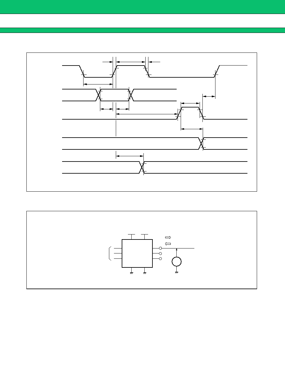
2. AC Characteristics
(V
DD
, V
CC
= +2.7 V to 3.6 V (V
CC
V
DD
), GND = V
SS
= 0 V, Ta = ≠20
∞
C to +85
∞
C)
Prameter
Symbol
Condition
Value
Unit
Min.
Max.
Clock L level pulse width
t
CKL
--
200
--
ns
Clock H level pulse width
t
CKH
--
200
--
ns
Clock rise time
Clock fall time
t
Cr
t
Cf
--
--
200
ns
Data setup time
t
DCH
--
30
--
ns
Data hold time
t
CHD
--
60
--
ns
Load setup time
t
CHL
--
200
--
ns
Load hold time
t
LDC
--
100
--
ns
Load H level pulse width
t
LDH
--
100
--
ns
Data output delay time
t
DO
See "∑ Load condition 1"
70
600
ns
D/A output settling time
t
LDD
See "∑ Load condition 2"
--
300
µ
s
∑ Load condition 1
Measurement point
C
L
= 20 pF
to 100 pF
∑ Load condition 2
R
AL
= 10 k
C
AL
= 50 pF
Measurement point

12
MB88346L
∑ Input/output timing
s
V
AO
VS
. I
AO
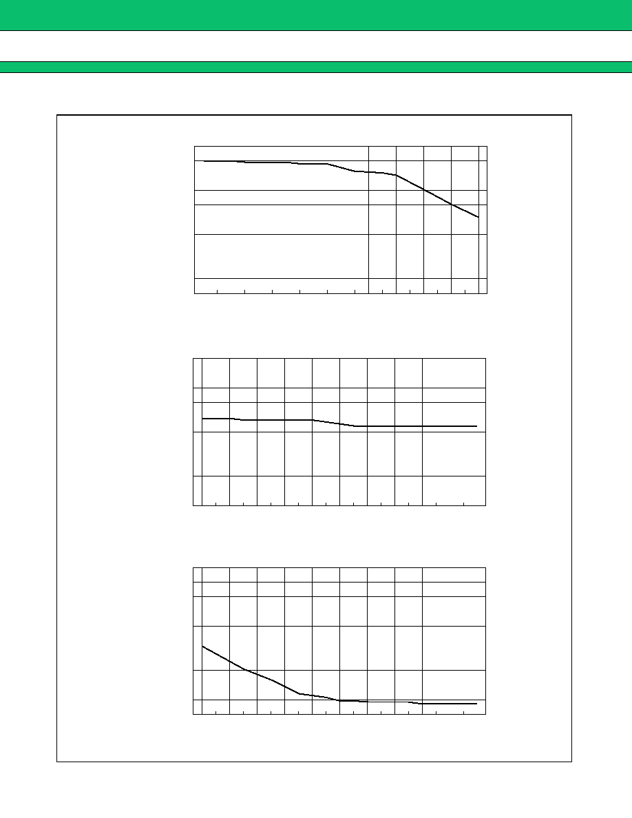
CHARACTERISTICS: EXAMPLE
(Continued)
CLK
DI
LD
D/A output
DO output
t
Cr
t
CKH
t
Cf
t
CKL
t
DCH
t
CHD
t
CHL
t
LDH
t
LDD
t
LDC
t
DO
Note: Decision levels: 80 % and 20 % of V
CC
90 %
10 %
3.0 V
3.0 V
MB88346L
Ta = +25∞C
Source current
Sink current
V
Pattern input
V
DD
DI
CLK
LD
V
SS
V
CC
AO1
AO12
GND
to

13
MB88346L
(Continued)
3,000
2,980
2,960
2,940
2,920
2,900
2,880
2,860
2,840
2,820
2,800
1.0
0.8
0.6
0.4
0.2
0.0
0.2
0.4
0.6
0.8
1.0
Sink current
Source current
[mA]
[mV]
Analog output level
#FF setting
1,600
1,580
1,560
1,540
1,520
1,500
1,480
1,460
1,440
1,420
1,400
1.0
0.8
0.6
0.4
0.2
0.0
0.2
0.4
0.6
0.8
1.0
[mA]
Sink current
Source current
[mV]
Analog output level
#80 setting
200
180
160
140
120
100
80
60
40
20
0
1.0
0.8
0.6
0.4
0.2
0.0
0.2
0.4
0.6
0.8
1.0
[mA]
Sink current
Source current
[mV]
Analog output level
#00 setting

14
MB88346L
s
ORDERING INFORMATION
Part number
Package
Remarks
MB88346LP
20-pin Plastic DIP
(DIP-20P-M02)
MB88346LPF
20-pin Plastic SOP
(FPT-20P-M01)
MB88346LPFV
20-pin Plastic SSOP
(FPT-20P-M03)

15
MB88346L
s
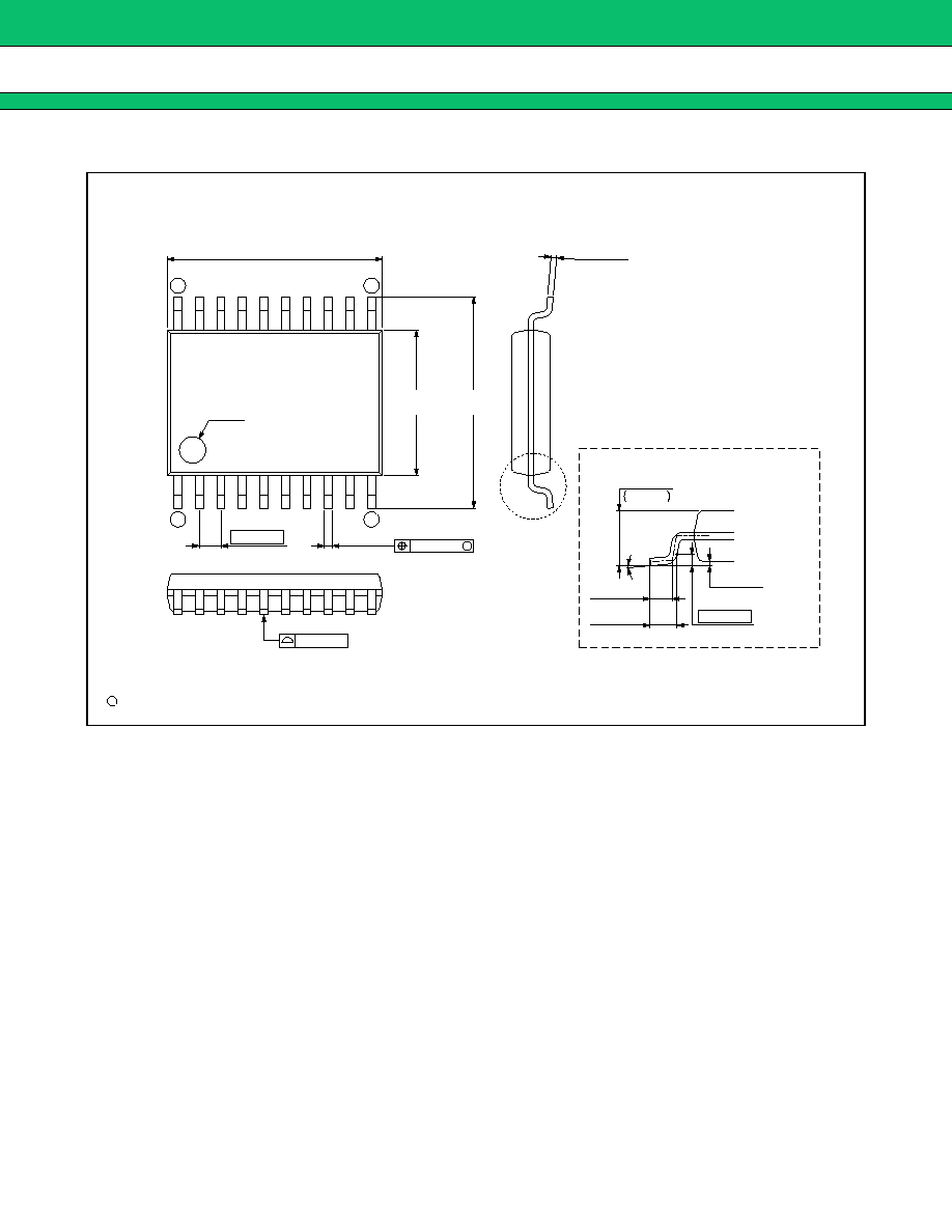
PACKAGE DIMENSIONS
(Continued)
C
1994 FUJITSU LIMITED D20003S-3C-4
0.46±0.08
(.018±.003)
INDEX-2
2.54(.100)
TYP
≠0.30
+0.20
24.64
15∞MAX
0.51(.020)MIN
(.010±.002)
0.25±0.05
1.27
+0.30
≠0
1.27(.050)
MAX
INDEX-1
≠0
+0.30
0.86
+.012
≠0
.034
.970
≠.012
+.008
6.20±0.25
(.244±.010)
7.62(.300)
TYP
4.36(.172)MAX
3.00(.118)MIN
.050
≠0
+.012
(FPT-20P-M02)
20-pin Plastic DIP
Dimensions in mm (inches).

16
MB88346L
(Continued)
C
1994 FUJITSU LIMITED F20003S-5C-4
0.10(.004)
ÿ0.13(.005)
M
"A"
0.68(.027)MAX
0.18(.007)MAX
0.20(.008)
0.50(.020)
Details of "A" part
0.45±0.10
0.05(.002)MIN
7.80±0.40
5.30±0.30
0.50±0.20
(.020±.008)
(STAND OFF)
(.018±.004)
(.209±.012)
(.307±.016)
.500
≠.008
+.010
≠0.20
+0.25
12.70
.006
≠.001
+.002
≠0.02
+0.05
0.15
.268
≠.008
+.016
≠0.20
+0.40
6.80
INDEX
TYP
1.27(.050)
11.43(.450)REF
2.25(.089)MAX
(Mounting height)
(FPT-20P-M01)
20-pin Plastic SOP
Dimensions in mm (inches)

17
MB88346L
(Continued)
C
1999 FUJITSU LIMITED F20012S-3C-5
6.50±0.10(.256±.004)
*
4.40±0.10
6.40±0.20
(.252±.008)
(.173±.004)
*
.049
≠.004
+.008
≠0.10
+0.20
1.25
(Mounting height)
0.10(.004)
0.65(.026)
0.24±0.08
(.009±.003)
1
10
20
11
"A"
0.10±0.10
(Stand off)
0.17±0.03
(.007±.001)
M
0.13(.005)
(.004±.004)
Details of "A" part
0~8∞
(.018/.030)
0.45/0.75
(.020±.008)
0.50±0.20
0.25(.010)
LEAD No.
INDEX
Dimensions in mm (inches)
Note 1) *:This dimension does not include resin protrusion.
Note 2) Pins width and pins thickness include plating thickness.
20-pin Plastic SSOP
(FPT-20P-M03)

MB88346L
FUJITSU LIMITED
All Rights Reserved.
The contents of this document are subject to change without notice.
Customers are advised to consult with FUJITSU sales
representatives before ordering.
The information and circuit diagrams in this document are
presented as examples of semiconductor device applications, and
are not intended to be incorporated in devices for actual use. Also,
FUJITSU is unable to assume responsibility for infringement of
any patent rights or other rights of third parties arising from the use
of this information or circuit diagrams.
The products described in this document are designed, developed
and manufactured as contemplated for general use, including
without limitation, ordinary industrial use, general office use,
personal use, and household use, but are not designed, developed
and manufactured as contemplated (1) for use accompanying fatal
risks or dangers that, unless extremely high safety is secured, could
have a serious effect to the public, and could lead directly to death,
personal injury, severe physical damage or other loss (i.e., nuclear
reaction control in nuclear facility, aircraft flight control, air traffic
control, mass transport control, medical life support system, missile
launch control in weapon system), or (2) for use requiring
extremely high reliability (i.e., submersible repeater and artificial
satellite).
Please note that Fujitsu will not be liable against you and/or any
third party for any claims or damages arising in connection with
above-mentioned uses of the products.
Any semiconductor devices have an inherent chance of failure. You
must protect against injury, damage or loss from such failures by
incorporating safety design measures into your facility and
equipment such as redundancy, fire protection, and prevention of
over-current levels and other abnormal operating conditions.
If any products described in this document represent goods or
technologies subject to certain restrictions on export under the
Foreign Exchange and Foreign Trade Law of Japan, the prior
authorization by Japanese government will be required for export
of those products from Japan.
F0001
©
FUJITSU LIMITED Printed in Japan


