 | –≠–ª–µ–∫—Ç—Ä–æ–Ω–Ω—ã–π –∫–æ–º–ø–æ–Ω–µ–Ω—Ç: FA3629AV | –°–∫–∞—á–∞—Ç—å:  PDF PDF  ZIP ZIP |

FA3629AV
1
s
Description
FA3629AV is a Power IC which includes DC-DC
converter controller and Nch-power MOSFET.
This IC can directly drive Nch/Pch MOSFET.
This IC is suitable to reduce converter size because it has
many functions in a small package TSSOP.
s
Features
∑ Low input voltage: 2.5V to 6.5V
∑ 40V CDMOS Process:
Built-in 0.3
Nch-Power MOSFET(ch1, open drain)
∑ 3-channels PWM Control:
2 boost circuits(ch1, ch2), 1 inverting circuit (ch3)
∑ Adjustable soft start time and maximum duty cycle
∑ Built-in timer latch for short circuit protection:
Delay time = 2
16
/ (switching frequency)
∑ Built-in protection functions: Overcurrent limit for MOSFET,
overheat protection, undervoltage lockout
∑ Wide range of operation frequency: 100kHz to 1MHz
∑ Package: TSSOP-16(Thin and small)
s
Applications
∑ Power supply for general equipment
s
Dimensions, mm
TSSOP-16
1
8
9
16
0~8∞
0.65
6.4
±
0.1
0.17
+0.02
4.4
5.2
0.2
±
0.05
0.5
±
0.08
1.1max
0.07
±
0.05
≠0.04
s
Block diagram
FA3629AV
CMOS IC
For Switching Power Supply Control
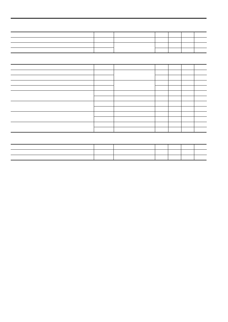
Pin
Pin
Description
No.
symbol
1
FB1
Ch.1 output of error amplifier
2
IN1≠
Ch.1 inverting input to error
amplifier
3
IN2≠
Ch. 2 inverting input to error
amplifier
4
GND
Ground of control blocks
5
PGND
Ground of large power blocks
6
FB2
Ch. 2 output of error amplifier
7
IN3≠
Ch. 3 inverting input to error
amplifier
8
FB3
Ch. 3 output of error amplifier
9
OUT3
Ch. 3 output (for Pch-MOSFET)
10
OUT2
Ch. 2 output (for Nch-MOSFET)
11
VCC
Power supply
12
OUT1
Ch.1 drain output of internal
Nch-MOSFET
13
REG
Regulated voltage output
14
CT
Oscillator timing capacitor
15
CS3
Soft start for Ch. 3
16
CS
Soft start for Ch.1 and Ch. 2

FA3629AV
2
Oscillator section
Item
Symbol
Test condition
Min.
Typ.
Max.
Unit
Oscillation frequency
f
OSC
C
T
=150pF
480
550
620
kHz
High level voltage
V
OSCH
C
T
=150pF
1.38
V
Low level voltage
V
OSCL
C
T
=150pF
0.78
V
Variation with supply voltage
f
dv
V
CC
=2.5 to 5.8V
1
2
%
Variation with temperature
f
dT1
Ta=≠20 to +25
∞
C
5
7
%
f
dT2
Ta=+25 to +85
∞
C
5
7
%
s
Recommended operating conditions
Item
Symbol
Min.
Max.
Unit
Power supply voltage
V
CC
2.5
5.8
V
Output voltage of OUT1
V
OUT1
0
32
V
Output current of OUT1
I
OUT1
0
1.8
A
Oscillation frequency
f
OSC
100
1000
kHz
Ambient temperature
T
OPR
≠20
85
∞
C
s
Absolute maximum ratings
Item
Symbol
Rating
Unit
Power supply voltage
V
CC
6.5
V
Output voltage at OUT1 pin
V
OUT1
40
V
Output current at OUT1 pin*
1
I
OUT1
2.8
A
Source peak current of OUT2
I
OUT2+
≠400
mA
Sink peak current of OUT2
I
OUT2
-
400
mA
Source peak current of OUT3
I
OUT3+
≠400
mA
Sink peak current of OUT3
I
OUT3
-
400
mA
Source average current of OUT2
I
OUT2+
≠50
mA
Sink average current of OUT2
I
OUT2
-
50
mA
Source average current of OUT3
I
OUT3+
≠50
mA
Sink average current of OUT3
I
OUT3
-
50
mA
Input voltage to err. amp.
V
EI
5.0
V
Total power dissipation*
2
P
d
500
mW
Ambient temperature
T
OPR
≠25 to +95
∞
C
Junction temperature
T
J
125
∞
C
Storage temperature
T
STG
≠40 to +125
∞
C
*
1
Output current is limited by the overcurrent protection
*
2
Ta < 25
∞
C
s
Electrical characteristics (V
CC
=3.0V, Ta=25
∞
C)
Reference voltage section
Item
Symbol
Test condition
Min.
Typ.
Max.
Unit
Reference voltage
V
REF
0.98
1.00
1.02
V
Variation with supply voltage
V
REF-LINE
V
CC
=2.5 to 5.8V
1
3
mV
Variation with temperature
V
REF-TC1
Ta=≠20 to +25
∞
C
0.5
1.2
%
V
REF-TC2
Ta=+25 to +85
∞
C
0.5
1.2
%
Regulated voltage for internal control blocks
Item
Symbol
Test condition
Min.
Typ.
Max.
Unit
Regulated voltage
V
REG
C
O
=0.1
µ
F
2.16
2.20
2.24
V
Variation with supply voltage
V
REG-LINE
V
CC
=2.5 to 5.8V
3
8
mV
Variation with temperature
V
REG-TC1
Ta=≠20 to +25
∞
C
0.5
1.5
%
V
REG-TC2
Ta=+25 to +85
∞
C
0.7
1.5
%
Source current
I
REG
≠40
≠15
mA

FA3629AV
3
Soft-start and duty section
Item
Symbol
Test condition
Min.
Typ.
Max.
Unit
Charge current of CS (Source)
I
CS
≠1.2
≠1.0
≠0.8
µ
A
Charge current of CS3 (Sink)
I
CS3
0.8
1.0
1.2
µ
A
Max. duty cycle of OUT1 & OUT2
D
max
f
OSC
=500kHz
80
87
90
%
Max. duty cycle of OUT3
D
max3
f
OSC
=500kHz
80
86
90
%
Invalid TL threshold voltage of CS
V
CSLO
0.42
0.52
0.62
V
Invalid TL threshold voltage of CS3
V
CSHI
1.58
1.68
1.78
V
Timer latch section (TL)
Item
Symbol
Test condition
Min.
Typ.
Max.
Unit
Threshold voltage of FB1 (Ch.1)
V
TLTH1
1.58
1.68
1.78
V
Threshold voltage of FB2 (Ch. 2)
V
TLTH2
1.58
1.68
1.78
V
Threshold voltage of FB3 (Ch. 3)
V
TLTH3
0.42
0.52
0.62
V
Start up count
count
≠
2
16
≠
counts
Start up time
T
TL
C
T
=150pF
105
119
137
ms
Error amplifier section
Item
Symbol
Test condition
Min.
Typ.
Max.
Unit
Input offset voltage
V
IO
10
mV
Common mode input voltage range
V
COM
0.2
1.5
V
DC open loop gain
A
VO
70
75
80
dB
Unity gain band width
f
T
1.0
1.7
2.0
MHz
Sink current (Ch.1)
I
OL1
V
FB1
=0.5V
1.0
1.5
2.0
mA
Source current (Ch.1)
I
OH1
V
FB1
=
V
REG
≠0.5V
≠160
≠120
≠80
µ
A
Sink current (Ch. 2)
I
OL2
V
FB2
=0.5V
0.5
0.7
0.9
mA
Source current (Ch. 2)
I
OH2
V
FB2
=
V
REG
≠0.5V
≠160
≠120
≠80
µ
A
Sink current (Ch. 3)
I
OL3
V
FB3
=0.5V
1.0
1.5
2.0
mA
Source current (Ch. 3)
I
OH3
V
FB3
=
V
REG
≠0.5V
≠160
≠120
≠80
µ
A
Sink current variation with temperature
I
OL-TC1
Ta=≠20 to +25
∞
C
20
%
I
OL-TC2
Ta=+25 to +85
∞
C
20
%
Source current variation with temperature
I
OH-TC1
Ta=≠20 to +25
∞
C
20
%
I
OH-TC2
Ta=+25 to +85
∞
C
20
%
Overcurrent protection section (OCP)
Item
Symbol
Test condition
Min.
Typ.
Max.
Unit
Threshold current
I
OCDTH
V
CC
=3.0V
1.4
1.8
2.0
A
V
CC
=5.0V
1.8
2.0
2.2
A
Delay time
f
OCD
100
200
400
ns
Undervoltage lockout circuit section (UVLO)
Item
Symbol
Test condition
Min.
Typ.
Max.
Unit
Threshold voltage of REG
V
UVTH
1.95
2.05
2.15
V
Overheat protection section (OHP)
Item
Symbol
Test condition
Min.
Typ.
Max.
Unit
Threshold temperature
T
OH
125
135
145
∞
C
FA3629AV
4
Output section (OUT1)
Item
Symbol
Test condition
Min.
Typ.
Max.
Unit
On resistance of MOSFET
R
ON1
V
CC
=3.0V,
I
O1
=200mA
0.25
0.275
0.3
Rise time of OUT1
t
r
V
CC
=3.0V
25
35
ns
Fall time of OUT1
t
f
V
OUT1
=10V, I
O1
=1.0A
25
35
ns
Overall device
Item
Symbol
Test condition
Min.
Typ.
Max.
Unit
Operating current (Overall)
I
CCA
D=50%,
f
OSC
=500kHz
3.0
3.8
mA
Operating current of control blocks
I
CTRL
1.8
mA
Output section (OUT2, OUT3)
Item
Symbol
Test condition
Min.
Typ.
Max.
Unit
Rise time of OUT2
t
r2
V
CC
=3V,
C
O2
=1000pF
20
25
35
ns
Fall time of OUT2
t
f2
(Between OUT2-GND)
20
25
35
ns
Rise time of OUT3
t
r3
V
CC
=3V,
C
O3
=1000pF
20
25
35
ns
Fall time of OUT3
t
f3
(Between VCC-OUT3)
20
25
35
ns
High level on resistance of OUT2
R
2AH
V
CC
=3V,
I
OUT2
=≠150mA
2.5
4.0
5.5
Low level on resistance of OUT2
R
2AL
V
CC
=3V,
I
OUT2
=
150mA
2.5
4.0
5.5
High level on resistance of OUT3
R
3AH
V
CC
=3V,
I
OUT3
=≠150mA
2.5
4.0
5.5
Low level on resistance of OUT3
R
3AL
V
CC
=3V,
I
OUT3
=150mA
2.5
4.0
5.5
High level on resistance of OUT2
R
2AH
V
CC
=5V,
I
OUT2
=≠150mA
2.0
3.5
5.0
Low level on resistance of OUT2
R
2AL
V
CC
=5V,
I
OUT2
=150mA
2.0
3.5
5.0
High level on resistance of OUT3
R
3AH
V
CC
=5V,
I
OUT3
=≠150mA
2.0
3.5
5.0
Low level on resistance of OUT3
R
3AL
V
CC
=5V,
I
OUT3
=150mA
2.0
3.5
5.0

FA3629AV
5
s
Characteristic curves (Ta=25
∞
C)
Supply current (I
CC
) vs oscillation frequency (f
OSC
)
Oscillation frequency (f
OSC
) vs. timing capactior(C
T
)
fosc [kH
Z
]
I
CC
[mA]
0
2
4
6
800k
200k
500k
V
CC
=2.5V
V
CC
=3.0V
V
CC
=5.0V
V
CC
=6.0V
Oscillation frequency (f
OSC
) vs. ambient temperature (Ta)
Max. on duty cycle vs. oscillation frequency (f
OSC
)
Ta [
∞
C]
fosc [kHz]
450
500
550
600
650
700
400
0
25
50
75
100
25
Oscillation peak voltage vs. timing capactior(C
T
)
Error amplifier voltage gain (Av) /phase vs.
frequency (f)
Condition: Open loop
C
T
[pF]
V
oltage [V]
0
1
2
1000
100
500
Maximum peak voltage
Minimum peak voltage
C
T
[pF]
fosc [kH
Z
]
100
1000
1000
100
fosc [kHz]
Maximum on duty cycle [%]
100
1000
500
70
80
90
100
CH.1, 2
CH. 3
A
V
[dB]
Phase [deg]
f [H
Z
]
100
1K
10K
100K
1M
10M
0
0
30
60
90
120
180
150
10
20
30
40
50
60
70
80
90
100
≠ 30
≠ 30
≠ 60
≠ 20
≠ 10
Av
Phase

FA3629AV
6
Output (Ch. 2) duty cycle vs FB terminal voltage (V
FB
)
Output (Ch. 3) duty cycle vs. FB3 terminal voltage (V
FB3
)
FB [V]
Output (CH. 2) duty cycle [%]
0
10
20
30
40
60
70
80
90
100
50
0.5
0.7
0.9
1.1
1.3
1.5
f
OSC
=150kH
Z
f
OSC
=550kH
Z
f
OSC
=800kH
Z
H-level output voltage (V
OH
) vs output source current (I
SO
)
L-level output voltage (V
OL
) vs. output sink current (I
SI
)
OUT2, OUT3
OUT2, OUT3
I
SO
[mA]
0
2.0
4.0
≠ 400
≠ 200
0
V
CC≠
V
OH
[V]
V
CC
=5.0V
V
CC
=3.0V
FB3 [V]
Output (CH. 3) duty cycle [%]
0
10
20
30
40
60
70
80
90
100
50
0.5
0.7
0.9
1.1
1.3
1.5
f
OSC
=150kH
Z
f
OSC
=550kH
Z
f
OSC
=800kH
Z
I
SI
[mA]
0
2.0
4.0
400
200
0
V
OL
[V]
V
CC
=5.0V
V
CC
=3.0V
FA3629AV
7
s
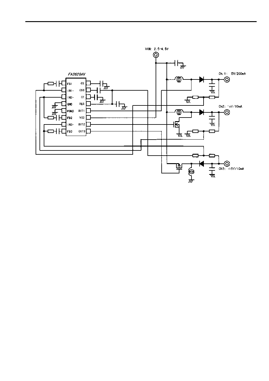
Application circuit
Parts tolerances characteristics are not defined in the circuit design
sample shown above. When designing an actual circuit for a product,
you must determine parts tolerances and characteristics for safe and
economical operation.