 | –≠–ª–µ–∫—Ç—Ä–æ–Ω–Ω—ã–π –∫–æ–º–ø–æ–Ω–µ–Ω—Ç: FA3630V | –°–∫–∞—á–∞—Ç—å:  PDF PDF  ZIP ZIP |

FA3630V
1
s
Description
FA3630V is a DC-DC converter controller.
This IC can directly drive a Nch/Pch-MOSFET.
This IC is suitable to reduce converter size because it has
many functions in a small package TSSOP.
s
Features
∑ Low input voltage: 2.5V to 6.5V
∑ 2-channels PWM control: Rail-to-rail output
Output impedance of output stage = 3.5
(typ.)
Nch-MOSFET driving (Ch1)
Nch/Pch-MOSFET driving (Ch2)(selected by SEL pin)
∑ Low power consumption: 0.7mA (typ.)
∑ ON/OFFcontrol: Standby current= 0.1
µ
A (typ.)
∑
±
2% high accuracy reference voltage
∑ Adjustable soft start time and maximum duty cycle
∑ Adjustable built-in timer latch for short circuit protection
∑ Wide range of operation frequency: 100kHz to 1MHz
∑ Package: TSSOP-16 (Thin and small)
s
Applications
∑ Power supply for general equipment
s
Dimensions, mm
TSSOP-16
1
8
9
16
0~8∞
0.65
6.4
±
0.1
0.17
+0.02
4.4
5.2
0.2
±
0.05
0.5
±
0.08
1.1max
0.07
±
0.05
≠0.04
s
Block diagram
FA3630V
CMOS IC
For Switching Power Supply Control
Pin
Pin
Description
No.
symbol
1
ON/OFF
ON/OFF function
2
IN2+
Ch. 2 non-inverting input to error
amplifier
3
IN2≠
Ch.2 inverting input to error
amplifier
4
FB2
Ch. 2 output of error amplifier
5
SEL
Selection of type of MOSFET
drived
6
GND
Ground
7
CS2
Soft start for Ch. 2
8
OUT2
Ch. 2 output (for Nch or Pch-
MOSFET)
9
OUT1
Ch.1 outout (for Nch-MOSFET)
10
CS1
Soft start for Ch.1
11
VCC
Power supply
12
VREG
Regulated voltage output
13
FB1
Ch.1 output of error amplifier
14
IN1≠
Ch.1 inverting input to error
amplifier
15
CP
Timing capacitor for timer latch
delay
16
CT
Oscillator timing capacitor

FA3630V
2
s
Electrical characteristics (V
CC
=3.3V, Ta=25
∞
C, C
T
=100pF)
Regulated voltage section for internal control blocks
Item
Symbol
Test condition
Min.
Typ.
Max.
Unit
Regulated voltage
V
REG
I
REG
=no load
2.156
2.200
2.244
V
Variation with output current
V
RGOUT
V
REG
=0 to 5mV
5
mV
Variation with supply voltage
V
RGLIN
V
CC
=2.5 to 5.5V
8
mV
Variation with temperature
V
RGTa
Ta=≠20 to +25
∞
C
±
0.5
%
Ta=+25 to +85
∞
C
±
0.5
%
Reference voltage section
Item
Symbol
Test condition
Min.
Typ.
Max.
Unit
Reference voltage
V
REF
0.98
1.00
1.02
V
Variation with supply voltage
V
RGLIN
V
CC
=2.5 to 5.5V
1
5
mV
Variation with temperature
V
RGTa
Ta=≠20 to +25
∞
C
±
0.5
%
Ta=+25 to +85
∞
C
±
0.5
%
s
Recommended operating conditions
Item
Symbol
Min.
Max.
Unit
Power supply voltage
V
CC
2.5
5.5
V
Input voltage for logic input
V
LOG
0
5.5
V
Oscillation frequency
f
OSC
100
1000
kHz
Oscillator section
Item
Symbol
Test condition
Min.
Typ.
Max.
Unit
Oscillation frequency
f
OSC
C
T
=100pF
437
485
533
kHz
High level voltage
V
OSCH
C
T
=100pF
1.39
V
Low level voltage
V
OSCL
C
T
=100pF
0.77
V
Variation with supply voltage
f
dV
V
CC
=2.5 to 5.5V
±
1
±
5
%
Variation with temperature
f
dT
Ta=≠20 to +25
∞
C
±
5
%
Ta=+25 to +85
∞
C
±
5
%
s
Absolute maximum ratings
Item
Symbol
Rating
Unit
Power supply voltage
V
CC
6.5
V
Source peak current of OUT1/2
I
OUT+
≠500
mA
Sink peak current of OUT1/2
I
OUT
≠
500
mA
Input voltage for logic input
V
LOG
≠0.3 to +6.5
V
Output current of VREG
I
REGMAX
≠10
mA
Total power dissipation*
P
d
300
mW
Junction temperature
T
J
125
∞
C
Ambient temperature
T
OP
≠20 to +85
∞
C
Storage temperature
T
stg
≠40 to +125
∞
C
*
Ta 25
∞
C
Error amplifier section
Item
Symbol
Test condition
Min.
Typ.
Max.
Unit
Input offset voltage
V
IOF
3
10
mV
Common mode input voltage
V
ICOM
0.2
1.5
V
DC open loop gain
A
VOL
70
75
dB
Unity gain band width
f
T
1.6
MHz
Output sink current
I
FBL
V
FB
=0.5V
2.0
2.5
3.0
mA
Output source current
I
FBH
V
FB
=
V
REG
≠0.5V
≠160
≠125
≠90
µ
A
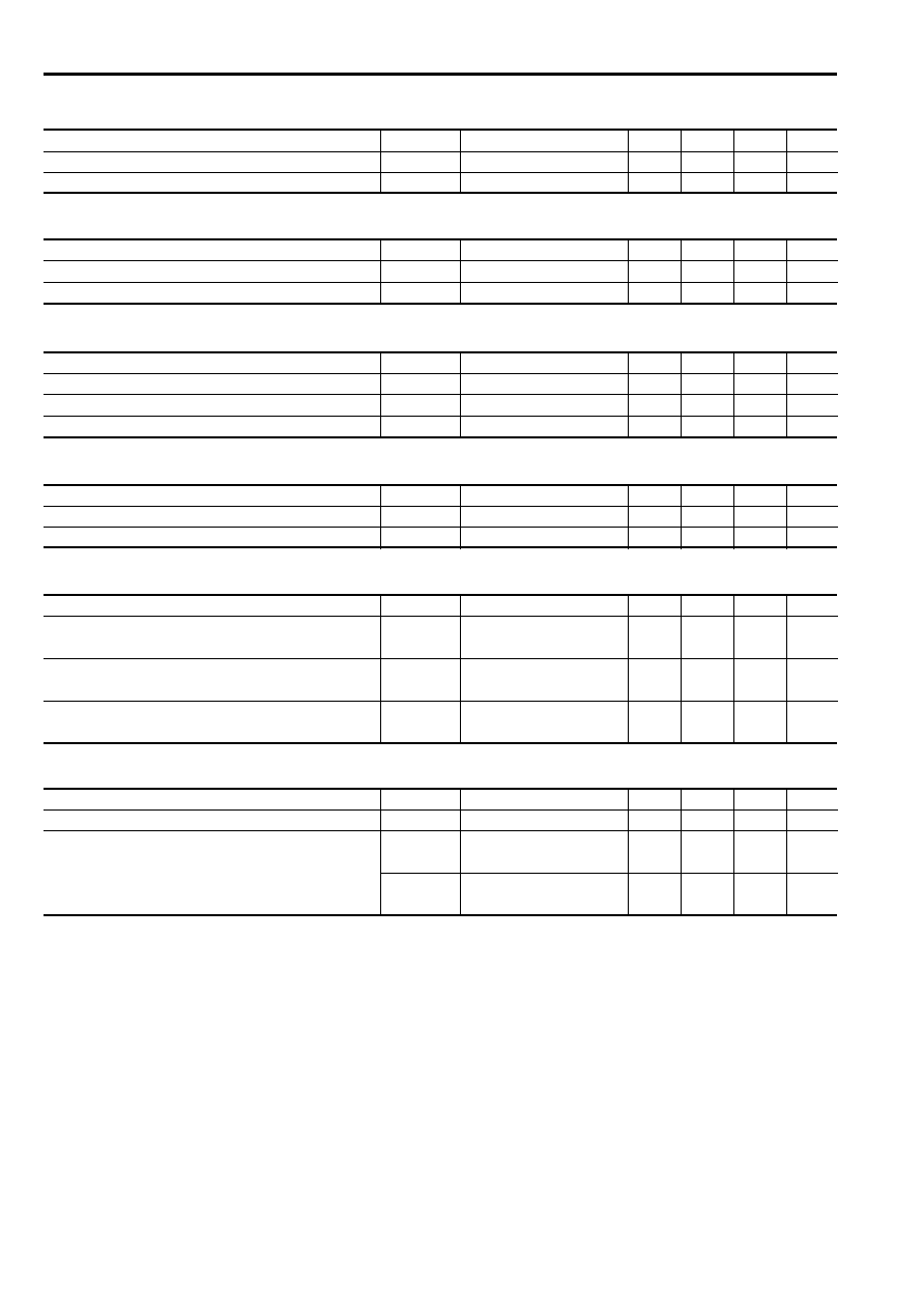
FA3630V
3
ON/OFF logic input signal section
Item
Symbol
Test condition
Min.
Typ.
Max.
Unit
Input range for ON mode
V
ONH
V
CC
=2.5V to 5.5V
2.0
V
Input range for OFF mode
V
ONL
V
CC
=2.5V to 5.5V
0.5
V
SEL logic input signal section
Item
Symbol
Test condition
Min.
Typ.
Max.
Unit
Input range for driving Nch-MOSFET
V
SELH
V
cc
≠0.5
V
Input range for driving Pch-MOSFET
V
SELL
0.5
V
Timer latch protection section
Item
Symbol
Test condition
Min.
Typ.
Max.
Unit
Threshold voltage of CP
V
CPTH
1.55
1.70
1.85
V
Charge current of CP
I
CP
V
CP=
V
REG
≠0.5V
≠2.5
≠2.1
≠1.7
µ
A
Threshold voltage of FB1/FB2
V
FBTL
1.56
1.73
1.90
V
Soft-start section
Item
Symbol
Test condition
Min.
Typ.
Max.
Unit
Threshold voltage of CS1/2
V
CS 0
Duty cycle=0%
0.74
0.79
0.84
V
Threshold voltage of CS1/2
V
CS 100
Duty cycle=100%
1.29
1.34
1.39
V
Overall device
Item
Symbol
Test condition
Min.
Typ.
Max.
Unit
Standby current
I
CC0
ON/OFF=GND
0.1
5
µ
A
Operating average current
I
CC
OUT1, OUT2: Open
0.7
1
mA
Output duty=100%
(Reference value) OUT1, OUT2: Open
1.5
mA
IN≠ and FB: Shorted
Output section
Item
Symbol
Test condition
Min.
Typ.
Max.
Unit
ON resistance
OUT1 ( High / Low )
R
ON
I
OUT
=
±
100mA
3.5
7
OUT2 ( High / Low )
V
CC
=3.3V
3.5
7
Rise time
OUT1
t
r
C
LOAD
=1000pF
25
35
ns
OUT2
V
CC
=3.3V
25
35
ns
Fall time
OUT1
t
f
C
LOAD
=1000pF
25
35
ns
OUT2
V
CC
=3.3V
25
35
ns
FA3630V
4
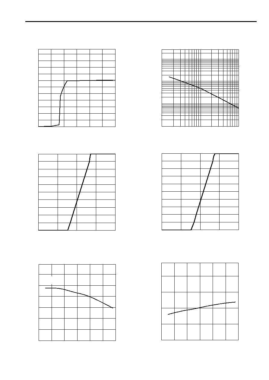
s
Characteristic curves (Ta=25
∞
C)
Supply current (I
CC
) vs. supply voltage (V
CC
)
Oscillation frequency (f
OSC
) vs. timing capactior(C
T
)
0
1
2
3
4
5
6
V
CC
[V]
I
CC
[mA]
0
0.1
0.2
0.3
0.4
0.5
0.6
0.7
0.8
0.9
1
1.1
Output duty cycle vs. FB terminal voltage (V
FB
)
Output duty cycle vs. CS terminal voltage (V
CS
)
0
0.5
1
1.5
2
V
FB
[V]
Output duty cycle [%]
0
10
20
30
40
50
60
70
80
90
100
Oscillation frequency (f
OSC
) vs. ambient temperature (Ta)
Reference voltage (V
REF
) vs. ambient temperature (Ta)
10
30
50
70
90
Ta [
∞
C]
f
OSC
[kH
Z
]
440
450
460
470
480
490
500
≠ 30
≠ 10
Vcc=3.3V
C
T
=100pF
0
0.5
1
1.5
2
V
CS
[V]
Output duty cycle [%]
0
10
20
30
40
50
60
70
80
90
100
10
30
50
70
90
Ta[
∞
C]
V
REF
[V]
0.99
0.995
1
1.005
1.01
≠ 30
≠ 10
10
100
500
1000
C
T
[pF]
fosc [kH
Z
]
10
100
1000
10000

FA3630V
5
L-level output voltage (V
OL1
) vs. output sink current (I
sink1
)
H-level output voltage (V
OH1
) vs. output source current (I
SOURCE1
)
0
50
100
150
200
250
300
I
SINK
1 [mA]
V
OL1
[V]
0
0.2
0.4
0.6
0.8
1
1.2
1.4
1.6
1.8
2
2.2
2.4
V
CC
=3.3V
L-level output voltage (V
OL2
) vs. output sink current (I
sink2
)
H-level output voltage (V
OH2
) vs. output source current (I
SOURCE2
)
0
50
100
150
200
250
300
I
SINK
2
[mA]
V
OL2
[V]
0
0.2
0.4
0.6
0.8
1
1.2
1.4
1.6
1.8
2
2.2
2.4
V
CC
=3.3V
Error amplifier voltage gain (Av) / phase (
) vs. frequency (f)
Condition: Open loop
[H
Z
]
[deg]
A
v
[dB]
0
20
40
60
80
100
120
140
160
180
100
1K
10K
100K
1M
10M
≠ 40
≠ 20
Voltage gain
Phase
2.2
2.4
0
50
100
150
200
250
300
I
SOURCE
1 [mA]
0
0.2
0.4
0.6
0.8
1
1.2
1.4
1.6
1.8
2
V
CC
=3.3V
V
CC≠
V
OH1
[V]
0
50
100
150
200
250
300
I
SOURCE
2 [mA]
0
0.2
0.4
0.6
0.8
1
1.2
1.4
1.6
1.8
2
2.2
2.4
V
CC
=3.3V
V
CC≠
V
OH2
[V]

FA3630V
6
s
Application circuit
Parts tolerances characteristics are not defined in the circuit design
sample shown above. When designing an actual circuit for a product,
you must determine parts tolerances and characteristics for safe and
economical operation.