FA3675F
122
s
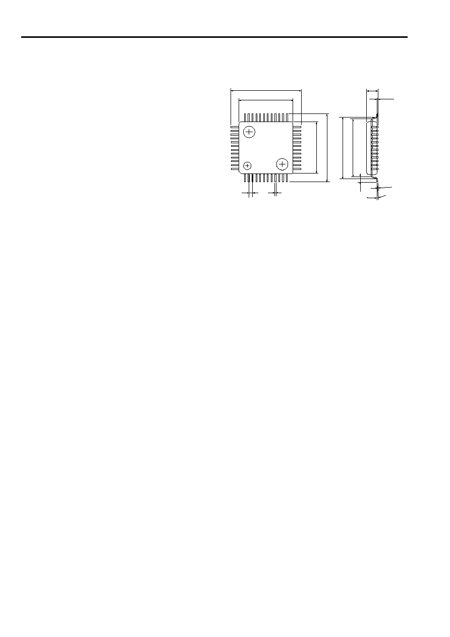
Dimensions, mm
LQFP-48
0~7∞
9.0
±
0.3
0.10
±
0.06
0.5
±
0.1
0.2
±
0.06
0.127
±
0.05
1.45 max
7.0
1
12
36
25
48
37
13
24
9.0
±
0.3
0.5
±
0.2
7.0
7.8
8.0
CMOS IC
For Switching Power Supply Control
s
Description
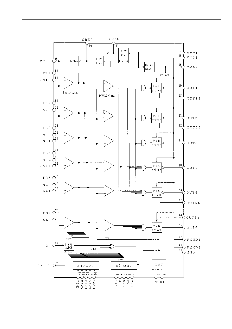
FA3675F is a control IC for 6-channel DC-DC converter.
This IC can directly drive a Nch/Pch-MOSFET.
This IC is suitable to reduce converter size because it has
many functions in a small package LQFP-48.
s
Features
∑ 6-channel PWM control with MOSFET direct driving :
5-channel for Pch-MOSFET, 1channel for Nch-MOSFET
∑ Low input voltage: 2.5V to 20V
∑
±
1.0% high accuracy bandgap reference
∑ Low power consumption by means of CDMOS
Standby mode: 20
µ
A(max.)
Operating mode: 10mA(max.)
∑ Soft start function for each channel
∑ ON/OFF function for each channel
∑ Timer latch for short protection
∑ Undervoltage lockout
∑ Wide range of operation frequency: 50kHz to 1MHz
∑ Package: LQFP-48(Thin and small)
s
Application
∑ VTR-camera, digital-steel-camera and portable equipment
FA3675F
FA3675F
124
*
Ta < 25
∞
C
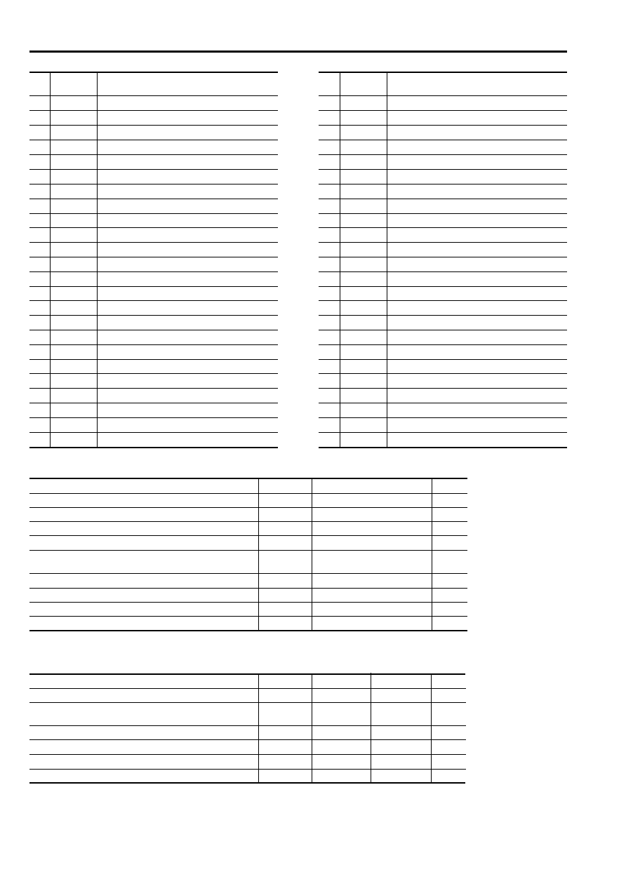
Pin
Pin
Description
No.
symbol
1
VCC1
Power supply for control circuit
2
RT
Oscillator timing resistor
3
CT
Oscillator timing capacitor
4
CS3
Soft start for Ch. 3 & Ch. 4
5
CS5
Soft start for Ch. 6
6
CS4
Soft start for Ch. 5
7
CS1
Soft start for Ch. 1
8
CS2
Soft start for Ch. 2
9
VREF
Reference voltage output
10
CREF
Capacitor for reference voltage output
11
VREG
Regulated voltage output
12
IN2-
Ch. 2 inverting input to error amplifier
13
FB2
Ch. 2 output of error amplifier
14
IN1-
Ch. 1 inverting input to error amplifier
15
FB1
Ch. 1 output of error amplifier
16
IN5+
Ch. 5 non-inverting input to error amplifier
17
IN5-
Ch. 5 inverting input to error amplifier
18
FB5
Ch. 5 output of error amplifier
19
IN6-
Ch. 6 inverting input to error amplifier
20
FB6
Ch. 6 output of error amplifier
21
IN3+
Ch. 3 non-inverting input to error amplifier
22
IN3-
Ch. 3 inverting input to error amplifier
23
FB3
Ch. 3 output of error amplifier
24
IN4+
Ch. 4 non-inverting input to error amplifier
Pin
Pin
Description
No.
symbol
25
IN4-
Ch. 4 inverting input to error amplifier
26
FB4
Ch. 4 output of error amplifier
27
CP
Timing capacitor for timer latch delay
28
GND
Ground
29
TLSEL
Ch. 3 & Ch. 4 timer latch selection (Low: disable)
30
CNT5
Ch. 6 ON/OFF function
31
CNT4
Ch. 5 ON/OFF function
32
CNT2
Ch. 2 ON/OFF function
33
CNT3
Ch. 3 & Ch. 4 ON/OFF function
34
CNT1
Ch. 1 ON/OFF function
35
VCC2
Power supply for output stage
36
VDRV
Bias for logic circuit of outputs
37
PGND1
Power ground
38
OUT1S
Ch. 1 source electrode of output stage
39
OUT1
Ch. 1 output (for Pch-MOSFET)
40
OUT4
Ch. 4 output (for Pch-MOSFET)
41
OUT3
Ch. 3 output (for Pch-MOSFET)
42
OUT2S
Ch. 2 source electrode of output stage
43
OUT2
Ch. 2 output (for Pch-MOSFET)
44
OUT6S
Ch. 6 source electrode of output stage
45
OUT6
Ch. 6 output (for Nch-MOSFET)
46
OUT5
Ch. 5 output (for Pch-MOSFET)
47
OUT5S
Ch. 5 source electrode of output stage
48
PGND2
Power ground
s
Absolute maximum ratings
Item
Symbol
Rating
Unit
Power supply voltage
V
CC
20.0
V
Source peak current
I
OUT
≠200
mA
Sink peak current
I
OUT
200
mA
Input voltage for analog input
V
ANA
≠0.3 to +2.5
V
Input voltage for logic input
V
LOG
≠0.3 to Vcc +0.5 (Vcc
5.0V)
V
≠0.3 to +5.5 (Vcc > 5.0V)
Total power dissipation
*
P
d
550
mW
Junction temperature
T
J
125
∞
C
Ambient temperature
T
OP
≠20 to +85
∞
C
Storage temperature
T
stg
≠40 to +150
∞
C
s
Recommended operating conditions
Item
Symbol
Min.
Max.
Unit
Power supply voltage
V
CC
2.5
18.0
V
Input voltage for logic input
Vcc
5.0
V
LOG
0.0
Vcc +0.25
V
Vcc > 5.0
0.0
5.25
Oscillation frequency
f
OSC
50
1000
kHz
Oscillator timing resistor
R
T
6.8
100
k
Oscillator timing capacitor
C
T
22
1000
pF
CREF terminal by-pass capacitor
C
REF
0.01
µ
F

FA3675F
125
Oscillator section
Item
Symbol
Test condition
Min.
Typ.
Max.
Unit
Oscillation frequency
f
OSC
R
T
=10k
,
C
T
=100pF
432
480
528
kHz
Frequency variation due to supply voltage change
f
dV
V
CC
=2.5 to 18V
±
1
±
3
%
Frequency variation due to temperature change
f
dT
T
a
=≠20 to +25
∞
C
±
3
±
6
%
T
a
=+25 to +85
∞
C
±
7
±
14
Error amplifier section
Item
Symbol
Test condition
Min.
Typ.
Max.
Unit
Input offset voltage
V
IOF
2
10
mV
Input common mode voltage range
V
ICOM
0.2
1.5
V
Open-loop gain
A
VOL
70
75
dB
Unity-gain bandwidth
f
T
1.0
MHz
Output sink current
I
FBL
V
FB
=
V
REF
+0.05V
2.5
3.5
mA
Output source current
I
FBH
V
FB
=
V
REF
-0.05V
≠0.18
≠0.14
mA
Soft-start circuit section 1 (CS1, CS2, CS3)
Item
Symbol
Test condition
Min.
Typ.
Max.
Unit
Input threshold voltage
V
CSO
Duty cycle=0%
0.36
0.46
0.56
V
V
CS100
Duty cycle=100%
1.11
1.31
1.51
V
Charge current
I
CS
V
CS
=0V
≠7.5
≠5.0
≠2.5
µ
A
Soft-start circuit section 2 (CS4, CS5)
Item
Symbol
Test condition
Min.
Typ.
Max.
Unit
Input threshold voltage
V
CSO
Duty cycle=0%
0.36
0.46
0.56
V
V
CS100
Duty cycle=100%
1.11
1.31
1.51
V
Charge current
I
CS
0
µ
A
s
Electrical characteristics (Ta=25
∞
C, Vcc
1
=Vcc
2
=6V, C
T
=100pF, R
T
=10k
)
Reference voltage section
Item
Symbol
Test condition
Min.
Typ.
Max.
Unit
Output voltage
V
REF
No load
0.99
1.00
1.01
V
Load regulation
V
RFLOD
No load to R
L
=15k
7
15
mV
Line regulation
V
RFLIN
V
CC
=2.5 to 18V
3
10
mV
Output voltage variation due to temperature change
V
RTa
T
a
=≠20 to +85
∞
C
±
0.5
±
1.0
%
Regulated voltage section
Item
Symbol
Test condition
Min.
Typ.
Max.
Unit
Output voltage
V
REG
No load
2.134
2.20
2.266
V
Load regulation
V
RG LOD
No load to R
L
=3.9k
2
10
mV
Line regulation
V
RG LIN
V
CC
=2.5 to 18V
6
20
mV
Output voltage variation due to temperature change
V
RGTa
T
a
=≠20 to +85
∞
C
±
0.5
±
1.0
%

FA3675F
126
Output section 4 (OUT6)
Item
Symbol
Test condition
Min.
Typ.
Max.
Unit
L-level ON resistance
R
ONL
I
O
=10mA, OUT6S:VCC2
10
15
H-level ON resistance
R
ONH
I
O
=≠10mA, OUT6S:VCC2
10
15
Rise time
tr
C
LOAD
=1000pF, OUT6S:VCC2
40
60
ns
Fall time
tf
C
LOAD
=1000pF, OUT6S:VCC2
70
95
ns
Source current
I
OUT
OUT6S:R
S6
=330
to VCC2
-14
-11
-8
mA
V
CC
=7V
Short-circuit protection section
Item
Symbol
Test condition
Min.
Typ.
Max.
Unit
Threshold voltage at CP
V
CPTH
1.39
1.64
1.89
V
Charge current at CP
I
CP
≠3.0
≠1.9
≠1.0
µ
A
Threshold voltage at error amplifier output
V
FBTL
1.36
1.56
1.76
V
ON/OFF logic input section
Item
Symbol
Test condition
Min.
Typ.
Max.
Unit
Input voltage for ON mode
V
DH
V
cc
5.0V
1.0
Vcc
V
+0.25
V
cc
>5.0V
1.0
5.25
Input voltage for OFF mode
V
DL
0
0.4
V
Undervoltage lockout circuit section
Item
Symbol
Test condition
Min.
Typ.
Max.
Unit
OFF to ON threshold voltage
V
UVVCC
1.52
1.72
1.92
V
Voltage hysteresis
UVCC
0.1
V
Output section 1 (OUT1)
Item
Symbol
Test condition
Min.
Typ.
Max.
Unit
L-level ON resistance
R
ONL
I
O
=10mA, OUT1S:GND
6
10
H-level ON resistance
R
ONH
I
O
=≠10mA, OUT1S:GND
6
10
Rise time
tr
C
LOAD
=1000pF, OUT1S:GND
30
50
ns
Fall time
tf
C
LOAD
=1000pF, OUT1S:GND
60
85
ns
Sink current
I
OUT
OUT1S:R
S1
=68
to GND
9
12
15
mA
Output section 2 (OUT2, OUT5)
Item
Symbol
Test condition
Min.
Typ.
Max.
Unit
L-level ON resistance
R
ONL
I
O
=10mA
10
15
OUT2S, OUT5S:GND
H-level ON resistance
R
ONH
I
O
=≠10mA
10
15
OUT2S, OUT5S:GND
Rise time
tr
C
LOAD
=1000pF
40
60
ns
OUT2S, OUT5S:GND
Fall time
tf
C
LOAD
=1000pF
70
95
ns
OUT2S, OUT5S:GND
Sink current
I
OUT
OUT2S, OUT5S:
8
11
14
mA
R
S2
, R
S5
=68
to GND
Output section 3 (OUT3, OUT4)
Item
Symbol
Test condition
Min.
Typ.
Max.
Unit
L-level ON resistance
R
ONL
I
O
=10mA
10
15
H-level ON resistance
R
ONH
I
O
=≠10mA
10
15
Rise time
tr
C
LOAD
=1000pF
40
60
ns
Fall time
tf
C
LOAD
=1000pF
70
95
ns
Overall device
Item
Symbol
Test condition
Min.
Typ.
Max.
Unit
Standby current
I
CCO
12
20
µ
A
Operating-state supply current
I
CC
Duty cycle=0%,
R
L=
4
6
mA