 | –≠–ª–µ–∫—Ç—Ä–æ–Ω–Ω—ã–π –∫–æ–º–ø–æ–Ω–µ–Ω—Ç: FA3686 | –°–∫–∞—á–∞—Ç—å:  PDF PDF  ZIP ZIP |
FA3686V
1
s
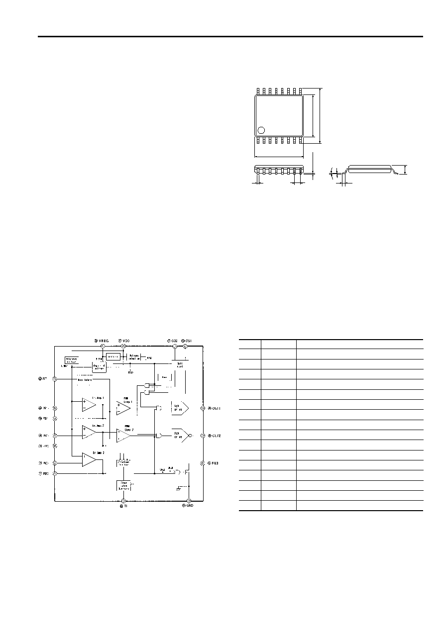
Block diagram
FA3686V
s
Dimensions, mm
TSSOP-16
s
Description
FA3686V is a PWM type DC-to-DC converter control IC with
2ch outputs that can directly drive power MOSFETs. CMOS
devices with high breakdown voltage are used in this IC and
low power consumption is achieved. This IC is suitable for very
small DC-to-DC converters because of their small and thin
package (1.1mm max.), and high frequency operation (to
1.5MHz). This IC contains built-in an error amplifier for series
regulators, therefore, this IC is suitable for the 3ch power supply
with a 2ch DC-to-DC converter and a 1ch series regulator.
s
Features
∑ Wide range of supply voltage: V
CC
=2.5 to 20V
∑ MOSFET direct driving
∑ Low operating current consumption by CMOS process:
3.0mA (typ.)
∑ 2ch PWM control IC
∑ High frequency operation: 300kHz to 1.5MHz
∑ Simple setting of operation frequency by timing resistor
∑ Built-in error amplifier for series regulator
∑ Soft start function on each channel (1ch, 2ch only)
∑ Maximum output duty cycle: 85% (typ.), at 500kHz
∑ Built-in under voltage lockout
∑ High accuracy reference voltage: VREF: 1.00V±1%,
V
REG
: 2.20V±1%
∑ Timer latch for short-circuit protection with counter
∑ PGS pin for a power supply fault signal
∑ Thin and small package: TSSOP-16
CMOS IC
For Switching Power Supply Control
Pin No. Pin symbol Description
1
FB3
Ch.3 output of error amplifier
2
IN3-
Ch.3 inverting input to error amplifier
3
FB2
Ch.2 output of error amplifier
4
IN2-
Ch.2 inverting input to error amplifier
5
PGS
PGS signal output
6
VCC
Power supply
7
CS2
Soft start for Ch.2
8
OUT2
Ch.2 output
9
OUT1
Ch.1 output
10
CS1
Soft start for Ch.1
11
GND
Ground
12
RT
Oscillator timing resistor
13
VREG
Regulated voltage output
14
IN1-
Ch.1 inverting input to error amplifier
15
FB1
Ch.1 output of error amplifier
16
TL
Timer latched short circuit protection
1
8
9
16
0
~
8
∞
0.65
6.4
±
0.2
0
.
1
0
5
t
o
0
.
1
4
5
4.4
5
0.22
±
0.02
0.5
±
0.08
1.1max
0.10
±
0.05
FA3686V
2
s
Recommended operating conditions
Item
Symbol
Test condition
Min.
Typ.
Max.
Unit
Supply voltage
V
CC
2.5
18
V
CS1, CS2, TL pin voltage
V
CTR_IN
0.0
2.5
V
IN1≠, IN2≠, IN3≠ pin voltage
V
EA_IN
0.0
2.5
V
Oscillation frequency
f
OSC
300
500
1500
kHz
VREG pin capacitance
C
REG
Vcc<10V
0.1
1.0
4.7
µF
10V Vcc<18V
0.47
1.0
4.7
µF
VREG pin current
I
REG
1.0
mA
VCC pin capacitance
C
VCC
1.0
µF
CS1 pin capacitance
C
CS1
Between CS1 and GND
0.01
µF
CS2 pin capacitance
C
CS2
Between CS2 and VREG
0.01
µF
s
Electrical characteristics (V
CC
=3.3V, C
REG
=1.0µF, R
T
=12k
, Ta=+25∞C)
Regulated voltage for internal control blocks (VREG pin)
s
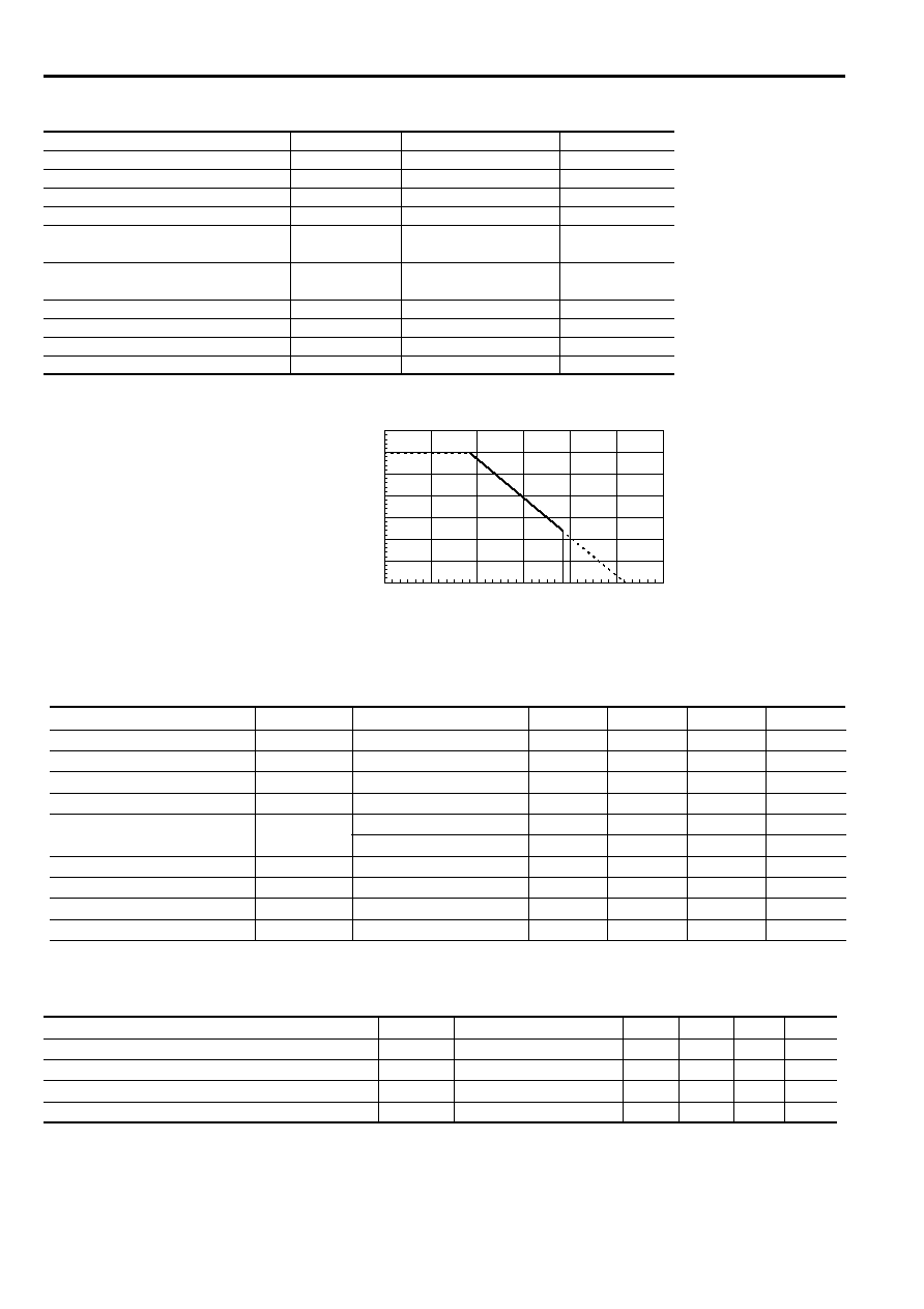
Absolute maximum ratings
Maximum power dissipation curve
I
tem
Symbol
Rating
Unit
Power supply voltage
V
CC
20
V
PGS pin voltage
V
PGS
20
V
FB1, IN1≠, FB2, IN2≠, FB3, IN3≠ pin voltage V
EA_IN
≠0.3 to 5.0
V
CS1, CS2, RT, TL, VREG pin voltage
V
CTR_IN
≠0.3 to 5.0
V
OUT1/2
OUT pin source current
I
OUT≠
≠400 (peak)
mA
OUT pin sink current
I
OUT+
150 (peak)
mA
OUT1/2
OUT pin source current
I
OUT≠
≠50 (continuous)
mA
OUT pin sink current
I
OUT+
50 (continuous)
mA
Power dissipation *
P
d
300 (Ta 25∞C)
mW
Operating junction temperature
T
J
+125
∞C
Operating ambient temperature
T
OPR
≠30 to +85
∞C
Storage temperature
T
STG
≠40 to +125
∞C
* Derating factor Ta 25∞C: 3mW/∞C
Item
Symbol
Test condition
Min.
Typ.
Max.
Unit
Regulated voltage
V
REG
2.178
2.200
2.222
V
Line regulation
V
REG_LINE
V
CC
=2.5 to 18V
±5
±15
mV
Load regulation
V
REG_LOAD
I
REG
=0 to 1mA
≠5
≠1
mV
Variation with temperature
V
REG_TC
Ta=≠30 to +85∞C
±0.5
%
0
50
100
150
200
250
300
350
-30
0
30
60
90
120
150
Ambient temperature [∞C]
Maximun power dissipation
[mW]
FA3686V
3
Error amplifier section (IN1≠, FB1, IN2≠, FB2, IN3≠, FB3 pin)
Item
Symbol
Test condition
Min.
Typ.
Max.
Unit
Reference voltage (CH.1)
V
REF1
*
1
0.99
1.00
1.01
V
Reference voltage (CH.2)
V
REF2
*
2
0.98
1.00
1.02
V
Reference voltage (CH.3)
V
REF3
*
3
0.98
1.00
1.02
V
V
REF
Line regulation
V
REF_LINE
V
CC
=2.5 to 18V
±2
±5
mV
V
REF
Variation with temperature
V
REF_TC1
Ta=≠30 to +85∞C
±0.5
%
Input bias current
I
IN≠
V
INx≠
=0.0 to 2.5V *
4
0.0
mA
Open loop gain
A
VO
70
dB
Unity gain bandwidth
f
T
1.5
MHz
Output current (sink)
I
SIFB
V
FBx
=0.5V, V
INx≠
=V
REG
*
4
2.3
3.5
4.7
mA
Output current (source)
I
SOFB
V
FBx
=V
REG
≠0.5V, V
INx≠
=0V *
4
≠360
≠270
≠180
µA
*
1
The FB1 voltage is measured under the condition that IN1- pin and FB1 pin are shorted. The input offset voltage of the error amplifier is included.
*
2
The FB2 voltage is measured under the condition that IN2- pin and FB2 pin are shorted. The input offset voltage of the error amplifier is included.
*
3
The FB3 voltage is measured under the condition that IN3- pin and FB3 pin are shorted. The input offset voltage of the error amplifier is included.
*
4
The "x" of INx- and FBx refers to 1 to 3.
Soft start section (CS1, CS2 pin)
Item
Symbol
Test condition
Min.
Typ.
Max.
Unit
Threshold voltage (CS1)
V
CS1D0
Duty cycle=0%, V
FB1
=1.4V
0.82
V
V
CS1D20
Duty cycle=20%, V
FB1
=1.4V
0.89
0.925
0.96
V
V
CS1D80
Duty cycle=80%, V
FB1
=1.4V
1.25
1.285
1.32
V
Threshold voltage (CS2)
V
CS2D0
Duty cycle=0%, V
FB2
=0.7V
1.33
V
V
CS2D20
Duty cycle=20%, V
FB2
=0.7V
1.20
1.235
1.27
V
V
CS2D80
Duty cycle=80%, V
FB2
=0.7V
0.84
0.875
0.91
V
Charge current of CS2 (source)
I
CS1
V
CS1
=0.5V
≠2.
≠2.0
≠1.5
µA
Charge current of CS2 (sink)
I
CS2
V
CS2
=V
REG≠
0.5V
1.5
2.0
2.4
µA
Pulse width modulation (PWM) section (FB1, FB2 pin)
Item
Symbol
Test condition
Min.
Typ.
Max.
Unit
Max. duty cycle of OUT1
D
MAX1
f
OSC
=300kHz
87
%
R
T
=12k
(f
OSC
500kHz)
80
85
90
%
f
OSC
=1.5MHz
78
%
Max. duty cycle of OUT2
D
MAX2
f
OSC
=300kHz
88
%
R
T
=12k (f
OSC
500kHz)
80
85
90
%
f
OSC
=1.5MHz
73
%
Threshold voltage of FB1
V
FB1D0
Duty cycle=0%
0.82
V
V
FB1D20
Duty cycle=20%
0.925
V
V
FB1D80
Duty cycle=80%
1.285
V
Threshold voltage of FB2
V
FB2D0
Duty cycle=0%
1.33
V
V
FB2D20
Duty cycle=20%
1.235
V
V
FB2D80
Duty cycle=80%
0.875
V
Oscillator section (RT pin)
Item
Symbol
Test condition
Min.
Typ.
Max.
Unit
Oscillation frequency
f
OSC
435
500
565
kHz
Line regulation
f
OSC_LINE
V
CC
=2.5 to 18V
±1
±5
%
Variation with temperature
f
OSC_TC1
Ta=≠30 to +85∞C
±3
%
FA3686V
4
PGS section (VCC, PGS pin)
Item
Symbol
Test condition
Min.
Typ.
Max.
Unit
Threshold voltage of VCC
V
PGS
V
CC
decreasing
2.15
2.25
2.35
V
Hysteresis voltage
V
PGS
V
CC
increasing
0.10
V
VPGS variation with temperature
V
PGS_TC1
Ta=≠30 to +85∞C
±1
%
On resistance
R
PGS
V
CC
=2.2V, I
PGS
=10mA
50
100
*
1
The latched mode operates when the voltage of FB1 or FB3 exceeds the threshold voltage as shown in the table.
*
2
The latched mode operates when the FB2 voltage falls below the threshold voltage as shown in the table.
*
3
The timer latch of FB1 is disabled when the CS1 voltage is below the threshold voltage as shown in the table.
*
4
The timer latch of FB2 is disabled when the CS2 voltage is above the threshold voltage as shown in the table.
Under voltage lockout circuit section (VCC pin)
Item
Symbol
Test condition
Min.
Typ.
Max.
Unit
ON threshold voltage of VCC
V
UVLO
2.0
2.2
2.35
V
Hysteresis voltage
V
UVLO
0.1
V
Timer latch protection section (TL pin)
Item
Symbol
Test condition
Min.
Typ.
Max.
Unit
Threshold voltage of FB1
V
THFB1TL
*
1
1.5
2.0
V
Threshold voltage of FB2
V
THFB2TL
*
2
0.2
0.6
V
Threshold voltage of FB3
V
THFB3TL
*
1
1.5
2.0
V
Threshold voltage of CS1
V
VTHCS1TL
*
3
0.2
0.6
V
Threshold voltage of CS2
V
VTHCS2TL
*
4
1.5
2.0
V
TL pin voltage for counting 16th stage
V
TL16
0
0.2
V
TL pin voltage counting 17th stage
V
TL17
V
REG≠
0.2
V
REG
V
* The "x" of OUTx refers to 1, 2.
Output section (OUT1, OUT2 pin)
Item
Symbol
Test condition
Min.
Typ.
Max.
Unit
High side on resistance of OUT1/2
R
ONHI
I
OUTx
=-50mA *
10
20
I
OUTx
=-50mA, V
CC
=5V *
9
I
OUTx
=-50mA, V
CC
=15V *
8
Low side on resistance of OUT1/2
R
ONLO
I
OUTx
=50mA *
5
10
I
OUTx
=50mA, V
CC
=5V *
5
I
OUTx
=50mA, V
CC
=15V *
5
Rise time of OUT1/2
t
RISE
C
L
=1000pF
25
ns
Fall time of OUT1/2
t
FALL
C
L
=1000pF
40
ns
Overall section
Item
Symbol
Test condition
Min.
Typ.
Max.
Unit
Supply current
I
CCA
Ch.1, Ch.2 operating mode
3.0
4.0
mA
I
CCA1
Ch.1, Ch.2 off mode
2.5
mA
I
CCA2
Ch.1, Ch.2 operating mode, V
CC
=18V
3.5
mA
I
CCA3
Latch mode
2.5
mA

FA3686V
5
s
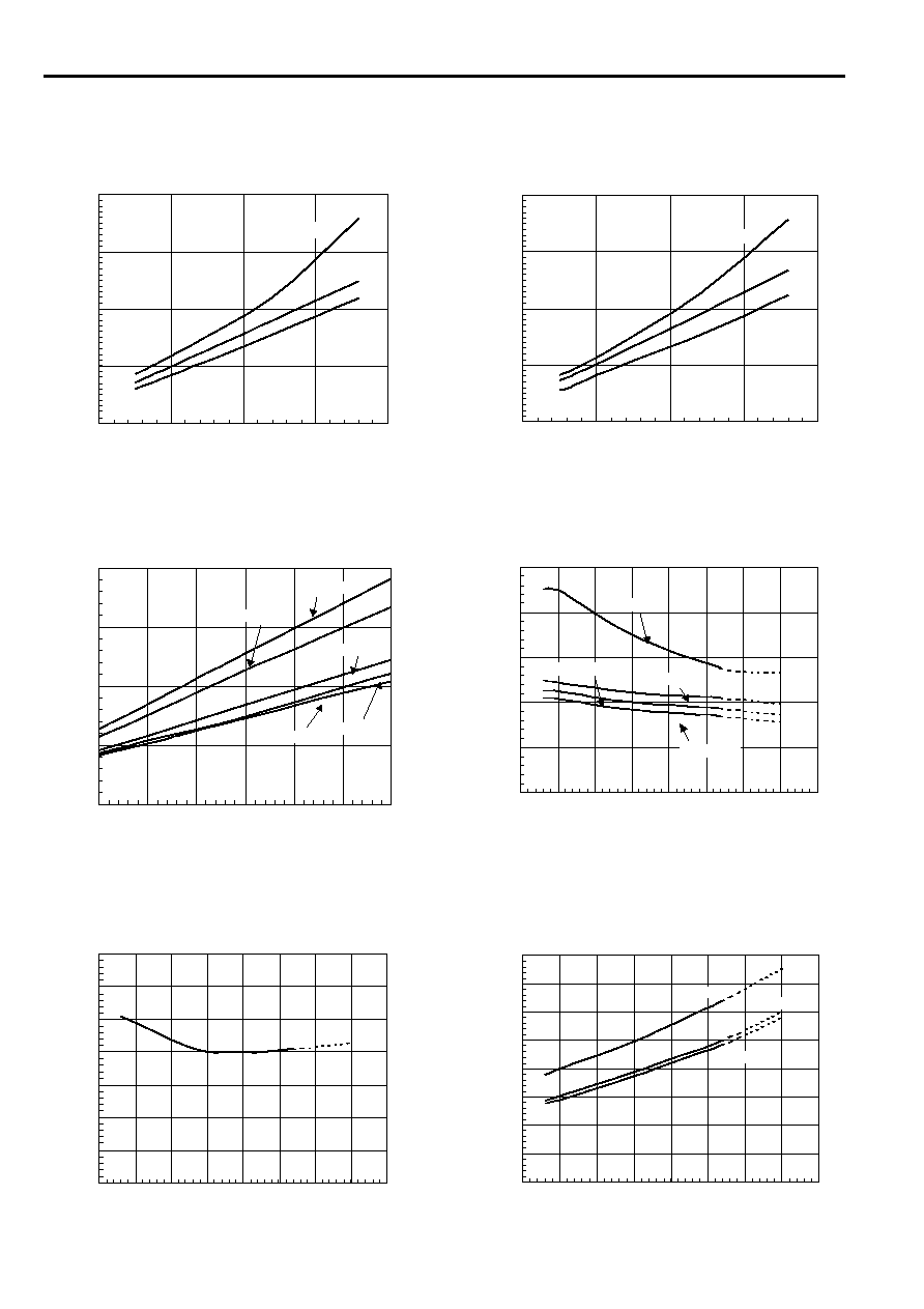
Characteristic curves
Oscillation frequency vs. timing resistor
Oscillation frequency vs. supply voltage V
CC
V
CC
=3.3V, Ta=25∞C
Ta=25∞C, R
T
=12k
(f
OSC
=500kHz)
Oscillation frequency vs. ambient temperature
Regulated voltage vs. supply voltage V
CC
V
CC
=3.3V, R
T
=12k
(f
OSC
=500kHz)
Ta=25∞C, R
T
=12k
(f
OSC
=500kHz)
Regulated voltage vs. ambient temperature
Regulated voltage vs. load current
V
CC
=3.3V, R
T
=12k
(f
OSC
=500kHz)
V
CC
=3.3V, R
T
=12k
(f
OSC
=500kHz)
0
200
400
600
800
1000
1200
1400
1600
1800
1
10
100
Timing resistor R
T
[k
]
Oscillation frequency [kHz]
490
492
494
496
498
500
502
504
506
508
510
0
5
10
15
20
Vcc [V]
Oscillation frequency [kHz]
430
450
470
490
510
530
550
570
-50
-25
0
25
50
75
100
125
150
Ambient temperature Ta [∞C]
Oscillation frequency [kHz]
2.17
2.18
2.19
2.20
2.21
2.22
2.23
0
5
10
15
20
Vcc [V]
Regulated voltage V
REG
[V]
Load current
I
REG
=0A
2.17
2.18
2.19
2.20
2.21
2.22
2.23
-50
-25
0
25
50
75
100
125
150
Ambient temperature Ta [∞C]
Regulated voltage V
REG
[V]
2.17
2.18
2.19
2.20
2.21
2.22
2.23
0.0
0.2
0.4
0.6
0.8
1.0
1.2
Load current I
REG
[mA]
Regulated voltage V
REG
[V]
Ta=-30∞C
Ta=25∞C
Ta=85∞C
FA3686V
6
Reference voltage vs. supply voltage V
CC
Reference voltage vs. ambient temperature
Ta=25∞C, R
T
=12k
(f
OSC
=500kHz)
V
CC
=3.3V, R
T
=12k
(f
OSC
=500kHz)
Error amp. output current (sink) vs. ambient temperature
Error amp. output current (source) vs. ambient temperarure
V
CC
=3.3V, R
T
=12k
(f
OSC
=500kHz)
V
CC
=3.3V, R
T
=12k
(f
OSC
=500kHz)
Charge current of CS1 (source) vs. ambient temperature
Charge current of CS2 (sink) vs. ambient temperature
V
CC
=3.3V, R
T
=12k
(f
OSC
=500kHz)
V
CC
=3.3V, R
T
=12k
(f
OSC
=500kHz)
0.980
0.985
0.990
0.995
1.000
1.005
1.010
1.015
1.020
0
5
10
15
20
25
Vcc [V]
Reference voltage V
REF
[V]
0.980
0.985
0.990
0.995
1.000
1.005
1.010
1.015
1.020
-50
-25
0
25
50
75
100
125
150
Ambient temperature Ta [∞C]
Reference voltage V
REF
[V]
2.0
2.5
3.0
3.5
4.0
4.5
5.0
-50
-25
0
25
50
75
100
125
150
Ambient temperature Ta [∞C]
Output current (sink) I
SIFB
[mA]
-350
-300
-250
-200
-150
-50
-25
0
25
50
75
100
125
150
Ambient temperature Ta [∞C]
Output current (source) I
SOFB
[uA]
-3.0
-2.5
-2.0
-1.5
-1.0
-50
-25
0
25
50
75
100
125
150
Ambient temperature Ta [∞C]
Charge current of CS1 (source) I
CS1
[uA]
1.0
1.5
2.0
2.5
3.0
-50
-25
0
25
50
75
100
125
150
Ambient temperature Ta [∞C]
Charge current of CS2 (sink) I
CS2
[uA]
FA3686V
7
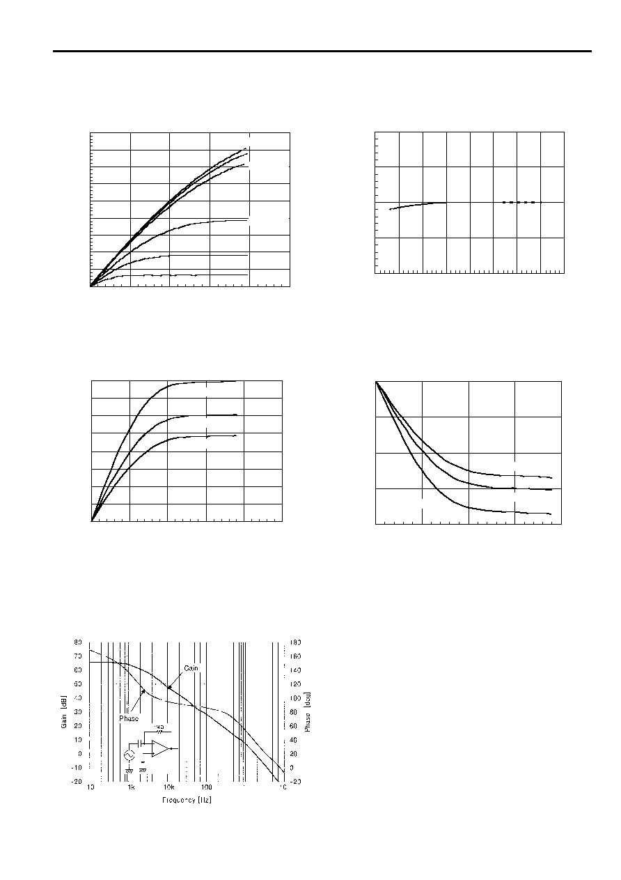
Output duty cycle vs. CS voltage (ch. 1)
Output duty cycle vs. oscillation frequency (ch. 1)
V
CC
=3.3V, Ta=25∞C
V
CC
=3.3V, Ta=25∞C
Output duty cycle vs. CS voltage (ch. 2)
Output duty cycle vs. oscillation frequency (ch. 2)
V
CC
=3.3V, Ta=25∞C
V
CC
=3.3V, Ta=25∞C
0
10
20
30
40
50
60
70
80
90
100
0.80
0.90
1.00
1.10
1.20
1.30
1.40
1.50
VCS1 [V]
Output duty cycle (ch.1) [%]
fosc=300kHz
fosc=500kHz
fosc=760kHz
fosc=1.5MHz
0
10
20
30
40
50
60
70
80
90
100
300
500
700
900
1100
1300
1500
Oscillation frequency [kHz]
Output duty cycle (ch.1) [%]
VCS1=0.85V
VCS1=0.90V
VCS1=0.95V
VCS1=1.00V
VCS1=1.05V
VCS1=1.10V
VCS1=1.15V
VCS1=1.20V
VCS1=1.25V
VCS1=1.30V
0
10
20
30
40
50
60
70
80
90
100
0.70
0.80
0.90
1.00
1.10
1.20
1.30
1.40
VCS2 [V]
Output duty cycle (ch.2) [%]
fosc=300kHz
fosc=500kHz
fosc=760kHz
fosc=1.5MHz
0
10
20
30
40
50
60
70
80
90
100
300
500
700
900
1100
1300
1500
Oscillation frequency [kHz]
Duty 2 [%]
VCS2=0.85V
VCS2=1.30V
VCS2=1.25V
VCS2=1.20V
VCS2=1.15V
VCS2=1.10V
VCS2=1.05V
VCS2=1.00V
VCS2=0.95V
VCS2=0.90V
Maximum duty cycle vs. oscillation frequency (ch. 1)
Maximum duty cycle vs. oscillation frequency (ch. 2)
V
CC
=3.3V, Ta=25∞C
V
CC
=3.3V, Ta=25∞C
65
70
75
80
85
90
95
300
500
700
900
1100
1300
1500
Oscillation frequency [kHz]
D
MAX1
[%]
65
70
75
80
85
90
95
300
500
700
900
1100
1300
1500
Oscillation frequency [kHz]
D
MAX2
[%]
FA3686V
8
Maximum duty cycle vs. ambient temperature (ch. 1)
Maximum duty cycle vs. ambient temperature (ch. 2)
V
CC
=3.3V, R
T
=12k
(f
OSC
=500kHz)
V
CC
=3.3V, R
T
=12k
(f
OSC
=500kHz)
OUT1 terminal source current vs. H level output voltage
OUT2 terminal source current vs. H level output voltage
Ta=25∞C
Ta=25∞C
80
81
82
83
84
85
86
87
88
89
90
-50
-25
0
25
50
75
100
125
150
Ambient temperature Ta [∞C]
D
MAX1
[%]
80
81
82
83
84
85
86
87
88
89
90
-50
-25
0
25
50
75
100
125
150
Ambient temperature Ta[∞C]
D
MAX2
[%]
OUT1 terminal source current vs. H level output voltage
OUT2 terminal source current vs. H level output voltage
V
CC
=3.3V
V
CC
=3.3V
-500
-450
-400
-350
-300
-250
-200
-150
-100
-50
0
0.0
1.0
2.0
3.0
4.0
5.0
6.0
Vcc-VOUT1 [V]
IOUT1 [mA]
Vcc=2.5V
Vcc= 3V
Vcc= 5V
Vcc=12V
-500
-450
-400
-350
-300
-250
-200
-150
-100
-50
0
0.0
1.0
2.0
3.0
4.0
5.0
Vcc-VOUT2 [V]
IOUT2 [mA]
Vcc=2.5V
Vcc= 3V
Vcc= 5V
Vcc=12V
-300
-250
-200
-150
-100
-50
0
0.0
0.5
1.0
1.5
2.0
2.5
3.0
Vcc-VOUT1 [V]
IOUT1 [mA]
Ta=-30∞C
Ta=25∞C
Ta=85∞C
-300
-250
-200
-150
-100
-50
0
0.0
0.5
1.0
1.5
2.0
2.5
3.0
Vcc-VOUT2 [V]
IOUT2 [mA]
Ta=-30∞C
Ta=85∞C
Ta=25∞C
FA3686V
9
OUT1 terminal source current vs. H level output voltage
OUT2 terminal source current vs. H level output voltage
V
CC
=12V
V
CC
=12V
-500
-400
-300
-200
-100
0
0.0
1.0
2.0
3.0
4.0
5.0
Vcc-VOUT1 [V]
IOUT1 [mA]
Ta=85∞C
Ta=-30∞C
Ta=25∞C
-500
-400
-300
-200
-100
0
0.0
1.0
2.0
3.0
4.0
5.0
Vcc-VOUT2 [V]
IOUT2 [mA]
Ta=-30∞C
Ta=25∞C
Ta=85∞C
OUT1 terminal sink current vs. L level voltage
OUT2 terminal sink current vs. L level voltage
OUT1 terminal rise time vs. supply voltage V
CC
OUT2 terminal rise time vs. supply voltage V
CC
C
L
=1000pF
C
L
=1000pF
0
50
100
150
200
0.0
0.2
0.4
0.6
0.8
1.0
1.2
1.4
VOUT1 [V]
IOUT1 [mA]
Ta=-30∞C
Ta=25∞C
Ta=85∞C
0
50
100
150
200
0.0
0.2
0.4
0.6
0.8
1.0
1.2
1.4
VOUT2 [V]
IOUT2 [mA]
Ta=-30∞C
Ta=85∞C
Ta=25∞C
0
10
20
30
40
50
60
0
5
10
15
20
Vcc [V]
OUT1 terminal rise time t
RISE
[ns]
Ta=-30∞C
Ta=25∞C
Ta=85∞C
0
10
20
30
40
50
60
0
5
10
15
20
Vcc [V]
OUT2 terminal rise time t
RISE
[ns]
Ta=25∞C
Ta=85∞C
Ta=-30∞C
FA3686V
10
OUT1 terminal fall time vs. supply voltage V
CC
OUT2 terminal fall time vs. supply voltage V
CC
C
L
=1000pF
C
L
=1000pF
Operating mode supply current vs. oscillation frequency
Operating mode supply current vs. ambient temperature
Ta=25∞C
UVLO ON threshold vs. ambient temperature
PGS terminal on resistance vs. ambient temperature
0
50
100
150
200
0
5
10
15
20
Vcc [V]
OUT1 terminal fall time t
FALL
[ns]
Ta=-30∞C
Ta=25∞C
Ta=85∞C
0
50
100
150
200
0
5
10
15
20
Vcc [V]
OUT2 terminal fall time t
FALL
[ns]
Ta=25∞C
Ta=-30∞C
Ta=85∞C
2.0
3.0
4.0
5.0
6.0
300
500
700
900
1100
1300
1500
Oscillation frequency [kHz]
Operating mode supply current I
CCA
[mA]
Vcc=12V
Vcc=18V
Vcc=2.5V
Vcc=5V
Vcc=3.3V
2.0
2.5
3.0
3.5
4.0
4.5
-50
-25
0
25
50
75
100
125
150
Ambient temperature Ta [∞C]
Operating mode supply current I
CCA
[mA]
Vcc=5V
Vcc=12V
Vcc=2.5V
Vcc=3.3V
1.8
1.9
2.0
2.1
2.2
2.3
2.4
2.5
-50
-25
0
25
50
75
100
125
150
Ambient temperature Ta [∞C]
UVLO ON threshold V
UVLO
[V]
0
10
20
30
40
50
60
70
80
-50
-25
0
25
50
75
100
125
150
Ambient temperature Ta [∞C]
R
PGS
[
]
Vcc=3.3V
Vcc= 5V
Vcc=2.5V
FA3686V
11
PGS terminal current vs. voltage
PGS terminal threshold voltage of VCC vs.
Ta=25∞C
ambient temperature
CS1 internal discharge switch current vs. voltage
CS2 internal discharge switch current vs. voltage
V
CC
=3.3V, R
T
=12k
(f
OSC
=500kHz)
V
CC
=3.3V, R
T
=12k
(f
OSC
=500kHz)
Error amplifier gain and phase vs. frequency
0
5
10
15
20
25
30
35
40
45
0.0
0.5
1.0
1.5
2.0
2.5
VPGS [V]
IPGS [mA]
Vcc=7.0V
Vcc=3.3V
Vcc=2.2V
vcc=1.8V
vcc=1.5V
Vcc=5V
2.15
2.20
2.25
2.30
2.35
-50
-25
0
25
50
75
100
125
150
Ambient temperature Ta [∞C]
V
PGS
[V]
0
50
100
150
200
250
300
350
400
0.00
0.50
1.00
1.50
2.00
2.50
V
CS1
[V]
ICS1 off [uA]
Ta=-30∞C
Ta=25∞C
Ta=85∞C
-200
-150
-100
-50
0
0.00
0.50
1.00
1.50
2.00
V
REG
-V
CS2
[V]
ICS2 off [uA]
Ta=-30∞C
Ta=25∞C
Ta=85∞C
FA3686V
12
s
Description of each circuit
1. Reference voltage circuit (V
REF
)
This circuit generates the reference voltage of 1.00V (ch1: ±1%;
ch2, 3: ±2%) compensated in temperature from V
CC
voltage,
and is connected to the non-inverting input of the error amplifier.
This voltage cannot be observed directly because an external
pin for this purpose is not provided.
2. Regulated voltage circuit (V
REG
)
This circuit generates 2.20V±1% based on the reference
voltage V
REF
, and is used as the power supply of the internal IC
circuits. This voltage is generated when the supply voltage,
V
CC
, is input. The V
REG
voltage also is used as a regulated
power supply for soft start and others. The output current for
external circuit should be within 1mA. A capacitor connected
between VREG pin and GND pin is necessary to stable the
V
REF
voltage (To determine capacitance, refer to recommended
operating conditions). The V
REG
voltage is regulated in V
CC
voltage of 2.4V or above.
3. Oscillator
The oscillator generates a triangular waveform by charging and
discharging the built-in capacitor. A desired oscillation
frequency can be set by the value of the resistor connected to
the RT pin (Fig. 1). The built-in capacitor voltage oscillates
between approximately 0.82V and 1.38V at fosc=500kHz (that
of ch1 and ch2 are slightly different) with almost the same
charging and discharging gradients (Fig. 2). You can set the
desired oscillation frequency by changing the gradients using
the resistor connected to the RT pin. (Large R
T
: low frequency,
small R
T
: high frequency) The oscillator waveform cannot be
observed from the outside because a pin for this purpose is not
provided. The RT pin voltage is approximately 1V DC in normal
operation. The oscillator output is connected to the PWM
comparator.
4. Error amplifier circuit
The error amplifiers 1, 2, 3 have inverting input pins of IN1≠ pin
(Pin 14), IN2≠ pin (Pin 4) and IN3≠ pin (Pin 2). The non-inverting
input is internally connected to the reference voltage V
REF
of the
error amplifier 1 (1.00V±1%; 25∞C) and the error amplifiers 2, 3
(1.00V±2%; 25∞C). The FB pins (Pin1, Pin15) are the output of
the error amplifiers. An external RC network is connected
between FB pin and IN≠ pin for gain and phase compensation
setting. The error amplifier 3 can be used for a series regulator.
Fig. 1
Fig. 2
12
OSC
R
T
R
T
R
T
value: small
R
T
value: large
0.82V
1.38V
+
14
15
3
13
IN1-
VREG
IN2-
FB2
FB1
Comp
Vout1
Vout2
R
NF
1
R
NF2
VREF
(1.0V)
R1
R2
R3
R4
4
2
1
R5
R6
R
NF3
FB3
Er.Amp.1
Er.Amp.2
Er.Amp.3
IN3-
Vout3
Fig. 3
FA3686V
13
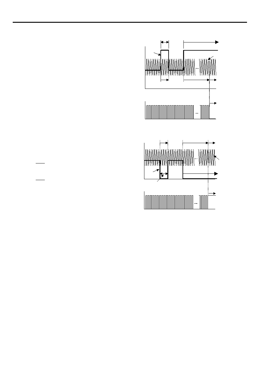
5. PWM comparator
The PWM output generates from the oscillator output, the error
amplifier output (FB1, FB2) and CS voltage (CS1, CS2) (Fig. 4).
The oscillator output is compared with the preferred lower
voltage between FB1 and CS1 for ch1. While the preferred
voltage is lower than oscillator output, the PWM output is low.
While the preferred voltage is higher than oscillator output, the
PWM output is high. Since the phase of Ch2 is the opposite
phase of Ch1, higher voltage between FB2 and CS2 is
preferred and while the preferred voltage is lower than the
oscillator output, the PWM output 2 is high. (Cannot be
observed externally) The output polarity of OUT1, OUT2
changes according to the condition of SEL pin. (See Fig. 6)
The maximum duty cycle (DMAX1, DMAX2) is internally set
approximately 85%. Note that the maximum duty cycle depends
on operation frequencies. (See the characteristics curve: Output
duty cycle vs. oscillation frequency)
6. Soft start function
This IC has a soft start function to protect DC-to-DC converter
circuits from damage when starting operation. CS1 pin (Pin10)
and CS2 pin (Pin7) are used for soft start function of ch1 and
ch2 respectively. (Fig. 5) When the supply voltage is applied to
the VCC pin and UVLO is cancelled, the capacitor C
CS1
and
C
CS2
is charged by the internal constant current sources (2µA,
typ.). Then, the CS1 voltage gradually increases, and the CS2
voltage gradually decreases. Since the CS1, and CS2 are
connected to the PWM comparator, the pulses gradually widen
and then the soft start function operates. (Fig. 6)
Fig. 4
Fig. 5
Nch.
drive
Pch.
drive
UVLO
Oscillator
output
CS1
CS2
FB2
FB1
OUT1
OUT2
PWM
Comp.1
PWM
Comp.2
PWM
output1
9
8
PWM output2
D
MAX1
D
MAX2
13
10
CS1
VREG
C
CS1
13
7
VREG
CS2
C
CS2
Oscillator output
CS1 pin voltage
Er. amp.1 output
PWM output 1
OUT1
Nch.drive
Oscillator output
CS2 pin voltage
Er. amp.2 output
PWM output2
OUT2
Pch. drive
Fig. 6
FA3686V
14
7. Timer latch short-circuit protection circuit
This IC has the timer latch short-circuit protection circuit. The
circuit cuts off the output of all channels when the output
voltage of DC-to-DC converter drops due to short circuit or
overload. Delay time of the timer latch mode is set by a counter
system in the internal circuit, therefore, no external parts are
necessary. When one of the output voltage of the DC-to-DC
converter drops due to a short circuit or overload, the FB1 and
FB3 pin voltage increases up to around the V
REG
voltage for
ch1 and ch3, or the FB2 pin voltage drops down to around 0V
for ch2.
The counter system operates when the FB1 or FB3 pin voltage
exceeds the timer latch threshold voltage of 2.0V(max.) or FB2
pin voltage falls below timer latch threshold voltage of
0.2V(min.). The counter system counts oscillator waveform. If
this system counts the oscillation cycles of 2
16
times (TL pin:
GND, 16th stage counter) or 2
17
times (TL pin: VREG, 17th
stage counter), this circuit detects short circuit. Then the IC is
set to off latch mode and the output of all channels is shut off
and the current consumption becomes 2.5mA (typ.). (Fig. 7)
If the DC-to-DC converters return to normal before counter
system counts 2
16
or 2
17
, counter is reset.
The period (tp) between the occurrences of short-circuit in the
converter output and setting to off latch mode can be calculated
by the following equations:
Example. When fosc=500kHz and TL pin to GND, the period tp is:
tp=2
16
1/500kHz=0.131sec.
You can reset off latched mode of the short-circuit protection by
either of the following ways to 1) CS pins, or 2) VCC pin:
1) Set the CS pin of the cause of off latch mode as follows.
CS1 pin voltage = 0V, CS2 pin voltage = VREG
2) V
CC
voltage is below UVLO off threshold voltage (2.1V typ.).
Connect the TL pin to either VREG or GND. If TL pin is
opened, the counter operation is unstable.
8. Output circuit
The IC contains a push-pull output stage and can directly drive
MOSFETs. The maximum peak current of the output stage is
sink current of +150mA, and source current of ≠400mA. The IC
can also drive NPN and PNP transistors. The maximum current
in such cases is ±50mA. You must design the output current
considering the rating of power dissipation. (See "Design
advice".)
9. Undervoltage lockout circuit
The IC contains an undervoltage lockout circuit to protect the
circuit from the damage caused by malfunctions when the
supply voltage drops. When the supply voltage rises from 0V,
the IC starts to operate at V
CC
of 2.2V (typ.) and outputs
generate pulses. If a drop of the supply voltage occurs, it stops
output at V
CC
of 2.1V (typ.). When it occurs, the CS1 pin is
turned to low level and the CS2 pin to high level, and then these
pins are reset.
Timer latch count
Timer latch count
Momentary
short circuit
Short circuit
Short circuit
protection
tp
FB1 or 3
Time t
Time t
Off latch mode
Oscillator output
OUT1
Timer latch
count
Timer latch
count
Momentary
short circuit
Short circuit
Short circuit
protection
tp
FB2
Time t
Time t
Off latch mode
OUT2
Oscillation output
Fig. 7
Ch1
Ch2
tp [s] = 2
16
1
fosc
TL pin: GND
tp [s] = 2
17
1
fosc
TL pin: VREG
FA3686V
15
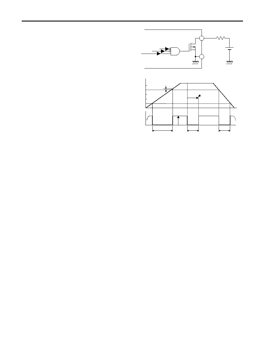
10. PGS circuit
The PGS pin is an open drain output of Nch MOSFET for
transmitting fault signals of the power supply. The PGS circuit is
enabled when Vcc voltage is over the operating threshold
voltage (approximately 1V). The Nch MOSFET turns ON and
the PGS pin is connected to GND if any of the following three
conditions occurs:
1) the V
CC
voltage is below the threshold voltage (V
CC
increasing: 2.35V typ.; V
CC
decreasing: 2.25V typ.), 2) UVLO
turns on (V
CC
=2.1V or below), 3) IC is off latch mode.
The operation sequence is shown in Fig. 8.
As shown in Fig. 8, in the case of increasing the Vcc voltage
with the voltage V applied to the PGS pin, when the Vcc voltage
reaches 1V, PGS circuit is enabled and detects that the Vcc
voltage is not enough high. Then PGS circuit turns the Nch
MOSFET on and output fault signal. The fault signal is
cancelled when the V
CC
voltage exceeds 2.35V (typ.).
In the case that the V
CC
voltage exceeds 2.53V (typ.) and the
IC is off latch mode, the PSG circuit detects it as abnormal and
the Nch MOSFET is turned on.
In the case of decreasing the V
CC
voltage, the circuit sends out
fault signals when the V
CC
voltage is below 2.25V (typ.) and
continues to output until the V
CC
voltage reaches below the
PGS circuit operation threshold voltage of approximately 1V.
(Under the V
CC
voltage of 1V, the circuit does not operate
normally.)
Fig. 8
+
5
PGS
11
V
UVLO
VPGS
Timer latch
V
CC
decreasing
V
CC
increasing
1V
V
PGS
voltage 2.25V
Hysteresis voltage
PGS
pin voltage
Vcc voltage stable state
Off latch mode
Off latch mode reset
PGS operation
PGS operation
PGS operation
Vcc
V
FA3686V
16
s
Design advice
1. Setting the oscillation frequency
As described in item 1, "Description of each circuit," a desired
oscillation frequency can be determined by the value of the
resistor connected to the RT pin. When designing an oscillation
frequency, you can set any frequency between 300kHz and
1.5MHz. You can obtain the oscillation frequency from the
characteristic curve "Oscillation frequency (fosc) vs. timing
resistor resistance (R
T
)" or the value can be approximately
calculated by the following expression.
This expression, however, can be used for rough calculation,
the obtain value is not guaranteed. The operation frequency
varies due to the conditions such as tolerance of the
characteristics of the ICs, influence of noises, or external
discrete components. When determining the values, examine
the effectiveness of the values in an actual circuit. The timing
resistor R
T
should be wired to the GND pin as shortly as
possible because the RT pin is a high impedance pin and is
easy affected by noises.
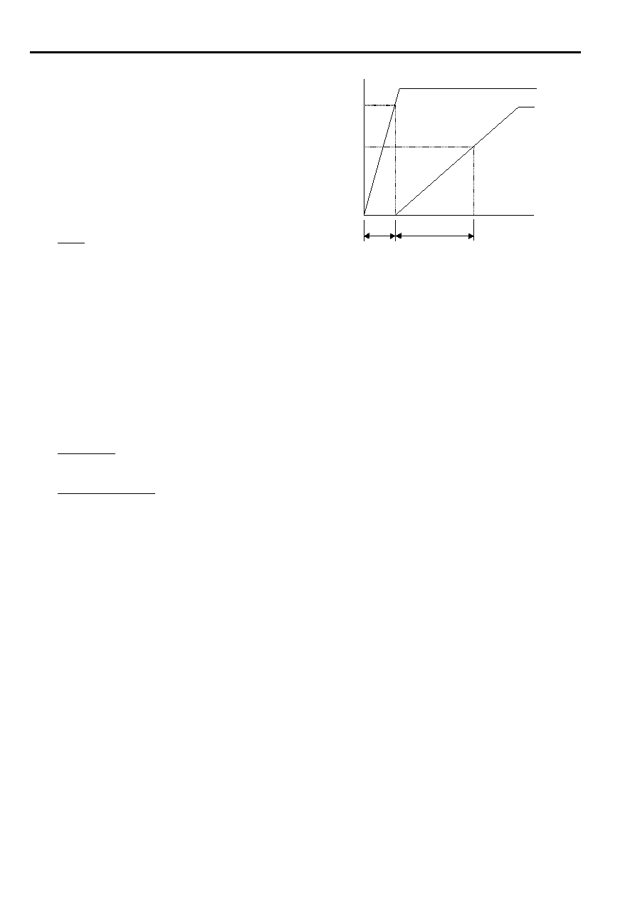
2. Determining soft start period
The period from the start of charging the capacitor C
CS
to
widening n% of output duty cycle can be roughly calculated by
the following expression: (see Fig. 5 for symbols)
V
CS1n
and V
CS2n
are the voltage of the CS1 and CS2 pins in
n% of output duty cycle, and vary in accordance with operating
frequency. The value can be obtained from the characteristic
curve "Output duty cycle vs. C
S
voltage"
The charging of the C
CS1
and C
CS2
starts after the UVLO is
unlocked. Therefore, the period from power-on of V
CC
to
widening n% of output duty cycle is the sum of t0 and t.
To reset the soft start function, the supply voltage V
CC
is
lowered below the UVLO voltage (2.1V typ.) and then the
internal switch discharges the CS capacitor. The characteristics
of the internal switch for discharge are shown in following the
characteristics curves of "Characteristics of CS1 internal
discharge switch current vs. voltage" and "Characteristics of
CS2 internal discharge switch current vs. voltage". Therefore,
when determining the period of soft start at restarting the power
supply, consider the characteristics carefully.
t [s] =
V
CS2n
C
CS1
I
CS1
For CS1 pin
t [s] =
(V
REG
≠ V
CS2n
)
C
CS1
I
CS2
For CS2 pin
C
CS1
, C
CS2
: Capacitance connected to the CS1 or CS2 pin [µF]
I
CS1
, I
CS2
:
CS charge current [µA] (2µA typ.)
f
OSC
= 4050
R
T
≠0.86
f
OSC
: Oscillation frequency [kHz]
RT:
Timing resistor [k
]
( )
RT =
4050
f
OSC
1.16
VCC pin voltage
CS1 pin voltage
Threshold
voltage
V
CS1n
t0
t
Fig. 9
FA3686V
17
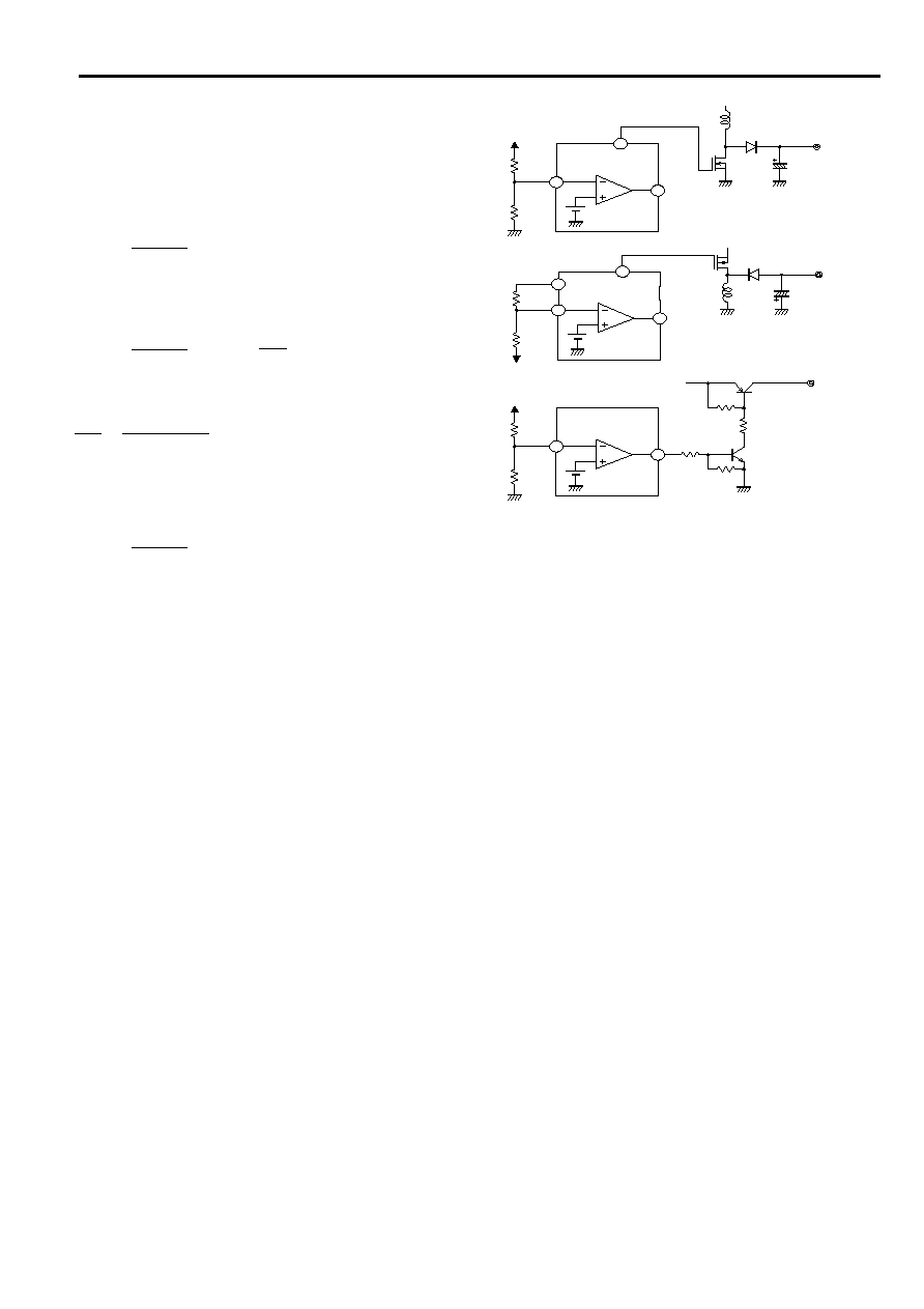
3. Determining the output voltage of DC-DC converters
The ways to determine the output voltage of the DC-DC
converter of each channel is shown in Fig. 10 and the following
equations.
For ch1:
The output voltage of a boost circuit is determined by:
For ch2:
The output voltage of an inverting circuit is determined by:
The ratio of resistances is determined by:
(Use the absolute value of the Vout2 voltage.)
For ch3:
The output voltage of a series regulator is determined by:
4. Restriction of external discrete components and
recommended operating conditions
To achieve a stable operation of the IC, the value of external
discrete components connected to VCC, VREG, CS pins should
be within the recommended operating conditions. And the
voltage and current applied to each pin should be also within the
recommended operating conditions. If the pin voltage of OUT1,
OUT2, or VREG becomes higher than the VCC pin voltage, the
current flows from the pins to the VCC pin because parasitic
three diode exist between the VCC pin and these pins. Be careful
not to allow this current to flow.
5. Loss calculation of IC
Since it is difficult to measure IC loss directly, the calculation to
obtain the approximate loss of the IC connected directly to a
MOSFET is described below.
When the supply voltage is V
CC
, the current consumption of the
IC is I
CCA
, the total input gate charge of the driven MOSFET is
Qg and the switching frequency is fsw, the total loss Pd of the IC
can be calculated by:
Pd V
CC
(I
CCA
+ Qg fsw).
The value in this expression is influenced by the effects of the
dependency of supply voltage, the characteristics of temperature,
or the tolerance of parameter. Therefore, evaluate the
appropriateness of IC loss sufficiently considering the range of
values of above parameters under all conditions.
Example:
I
CCA
=3.0mA for V
CC
=3.3V in the case of a typical IC from the
characteristics curve. Qg=6nC, fsw=500kHz, the IC loss "Pd" is
as follows.
Pd 3.3 (3.0mA + 6nC 500kHz) 19.8mW
If two MOSFETs are driven under the same condition for 2
channels, Pd is as follows:
Pd 3.3 {3.0mA + 2 (6nC 500kHz)} = 29.7mW
IN1-
FB1
Vout1
R2
R1
OUT1
Vout1
9
15
14
+
VREF
(1.0V)
IN2-
FB2
Vout2
R4
R3
OUT2
Vout2
8
3
4
+
VREF
(1.0V)
VREG
13
IN3-
FB3
Vout3
R6
R5
Vout3
1
2
+
VREF
(1.0V)
Vout1 =
R1 + R2
V
REF
R2
Vout2 =
R3 + R4
V
REF
≠
R4
V
REG
R3
R3
Vout3 =
R5 + R6
V
REF
R6
R3
=
V
REG
≠ V
REF
R3
Vout2 + V
REF
Fig. 10
FA3686V
18
s
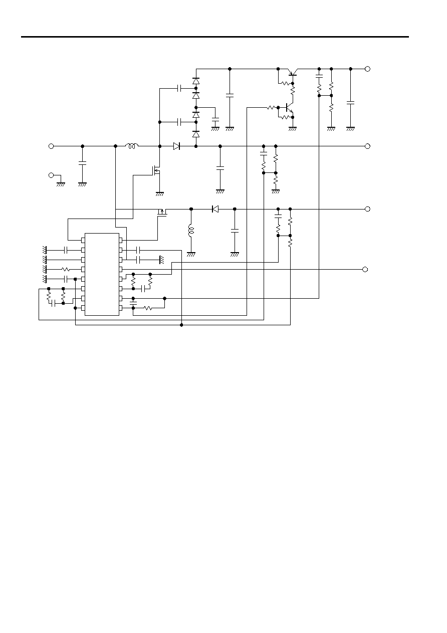
Application circuit
4700pF
0.47uF
2200pF
0.047uF
1uF
0.022uF
4700pF
10k
4.7k
10k
12k
0.1uF
0.1uF
180k
13k
10k
4700pF
4k
1k
470
1000pF
11k
2.2k
470
1000pF
10uF
2.9 to 3.6V
10V/5mA
5.0V/200mA
-5.0V/100mA
PGS
GND
4.7uF
15uF
10uF
0.1uF
0.1uF
FB1
IN1-
IN2-
GND
PGS
FB2
IN3-
FB3
CS1
CS2
RT
VREG
OUT1
VCC
OUT2
TL
FA3686V
15
14
11
10
12
13
9
16
4
5
3
2
1
7
6
8
47k
33k
Parts tolerances characteristics are not defined in the circuit design
sample shown above. When designing an actual circuit for a product,
you must determine parts tolerances and characteristics for safe and
economical operation.